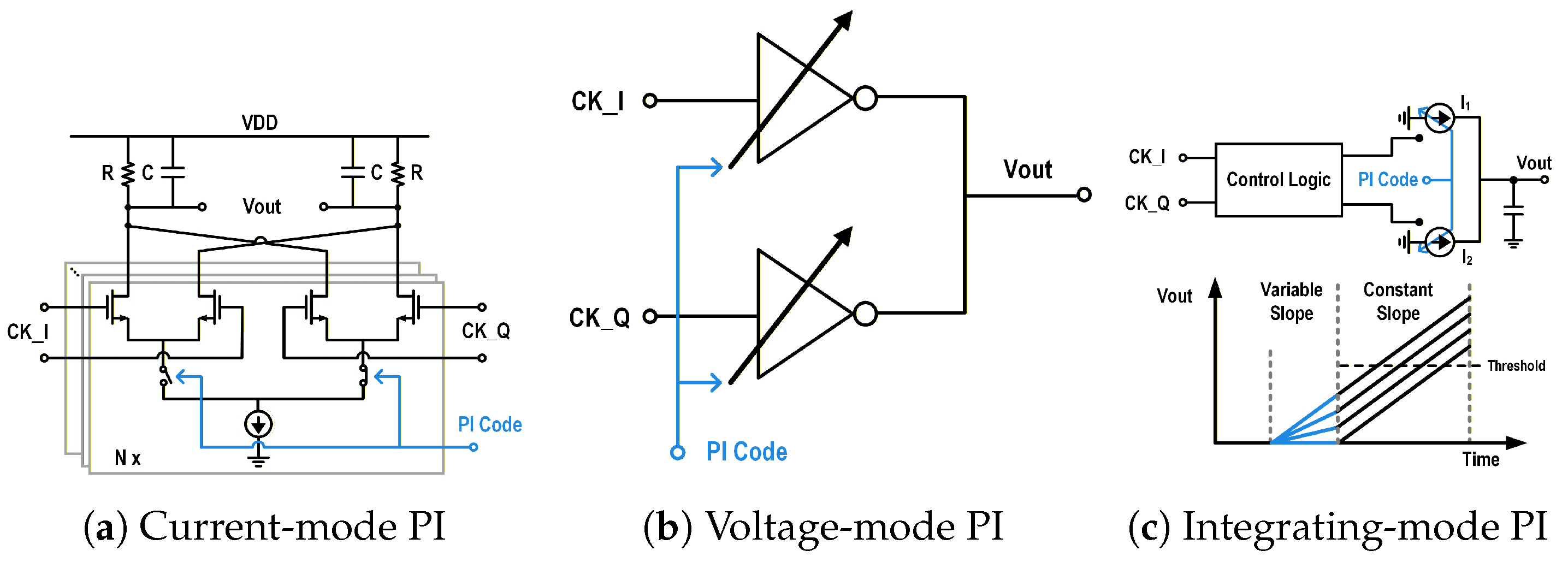
The integrating-mode PI (IMPI) presents a promising alternative. As shown in the generic architecture in
Figure 1c, the IMPI operation toggles between a variable region and a constant region, governed by the input clocks (CK_I and CK_Q). In the variable-slope region, the digital PI code modulates the integration current magnitude, charging (or discharging) the load capacitor
at different rates to establish a code-dependent linear voltage level. Subsequently, in the constant-slope region,
is charged (or discharged) by a fixed current. This constant slew rate translates the previously established linear voltage difference into a linear time delay. This mechanism offers the potential for fundamentally better linearity with only quadrature inputs, typically leading to lower power consumption and a smaller area compared to its counterparts. For these reasons, the IMPI topology is chosen for this work.
Recent research has focused on improving the speed and resolution of IMPIs. While early architectures were often limited by complex control logic and feedback loops, a significant advancement presented in [
8] achieved an impressive 14 GHz operation by removing these elements. However, this performance is predicated on a critical prerequisite: high slew-rate input clocks (i.e., “square-wave-like” waveforms with a rise/fall time of less than
, where
T is the period of input clocks). Preserving such fast transitions requires wide signal bandwidths, which is challenging and power-intensive to maintain in multi-gigahertz distribution networks. This requirement has become a major bottleneck limiting the application of high-speed IMPIs in even higher frequency domains. Furthermore, to achieve lower INL change from the process variation, Ref. [
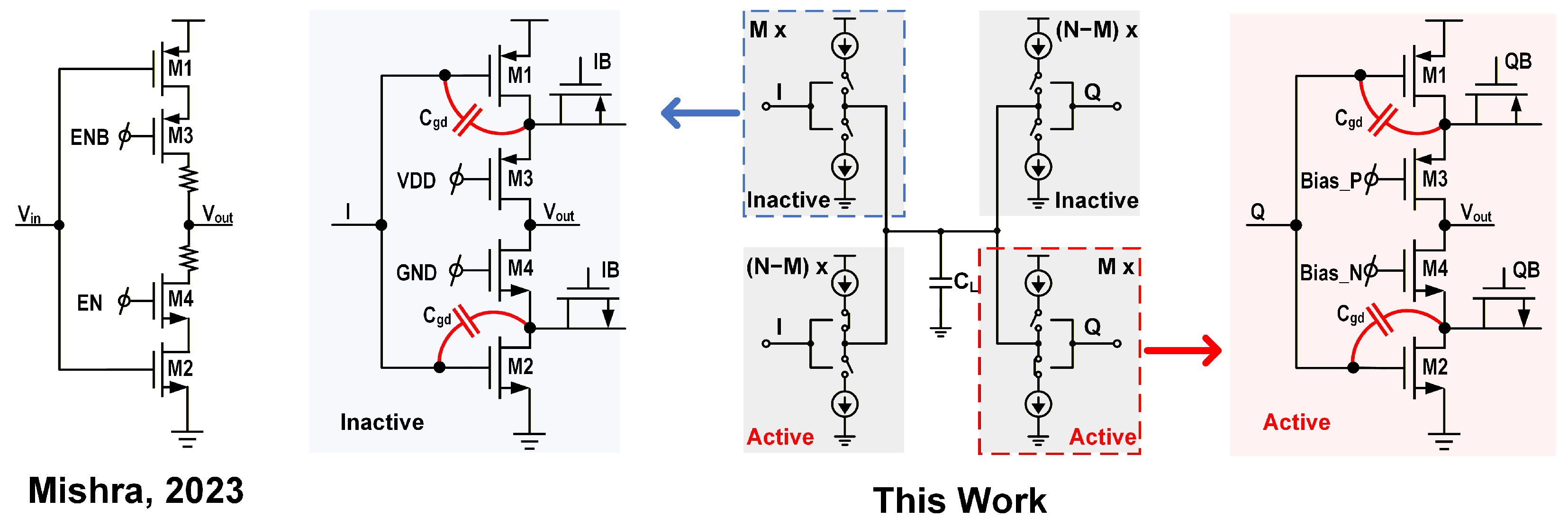
8] has employed slice architectures using transistor and resistor stacking (as shown in
Figure 2). While this topology is effective for stabilizing output impedance, it requires a resistor value comparable to the transistor’s
. This large resistance consumes significant voltage headroom (
), which is a critical concern in modern low-voltage FinFET processes.
This work is therefore motivated by the need to overcome this fundamental limitation. The primary goal is to develop an IMPI architecture that can achieve high-speed, low-jitter performance while releasing the stringent requirement on input bandwidth, enabling it to operate with more practical slew-rate-limited inputs. A pure sine-wave, having a continuously varying and limited slew rate, is considered as the representative worst-case for the following theoretical analysis.
2.1. Proposed Circuit Architecture and Operation
The proposed 9-bit PI is implemented using a coarse-fine architecture consisting of a 2-bit MUX and a 7-bit PI core. The interpolation process begins with the MUX, which receives the quadrature clocks and performs a coarse 2-bit interpolation by selecting two adjacent phases. These selected phases are subsequently sharpened by an inverter-based buffer to generate steeper edges. Finally, the edge-sharpened clocks are fed into the 7-bit PI core, which performs the fine-grained 7-bit interpolation. This hierarchical structure combines the 2-bit coarse and 7-bit fine stages to achieve the full 9-bit resolution.
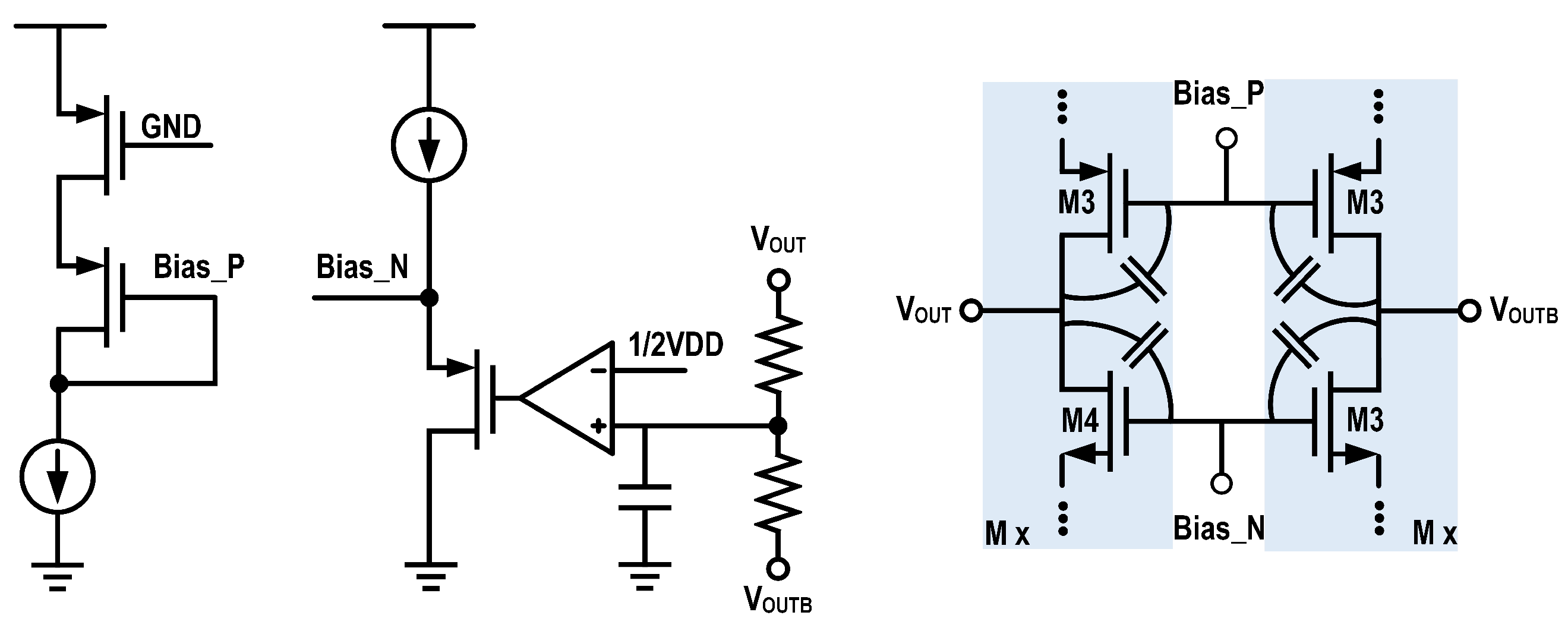
The 7-bit PI core architecture and the schematic of its unit slice are shown in
Figure 2. The core consists of arrays of identical unit slices connected to a shared load capacitor,
. As depicted in the central part of the figure, the 7-bit fine-interpolation code M partitions the total N (where N
) slices within the core into groups of M and (N-M), which are then selectively activated to perform a weighted current integration.
Each unit slice is based on a compact 4-transistor cell designed for high-speed operation. The mechanism for activating and deactivating a slice is also illustrated in
Figure 2. In the “Active” state, the gates of the current-source transistors (M3 and M4) are connected to the analog bias voltages “Bias_P” and “Bias_N”. In this state, M3/M4 function as a current source/sink pair, while M1/M2 act as input switches, allowing the slice to contribute its unit current to the output node ‘Vout’. Conversely, in the “Inactive” state, the gates of M3 and M4 are connected to VDD and GND, respectively, which reliably turns the current sources off and disconnects the slice from the interpolation operation.
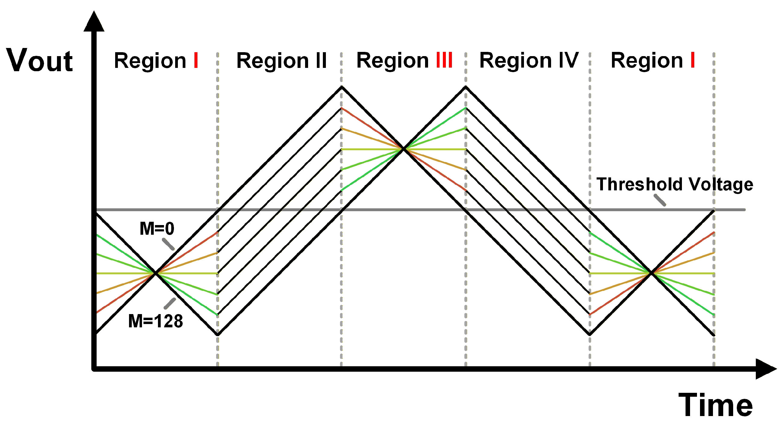
This architecture, controlled by the quadrature input clocks, sequentially activates different combinations of slices. This generates the ideal triangular voltage waveform across the load capacitor (
), as shown in
Figure 3. In the variable-slope regions (Regions I and III), the integration slope is dependent on the digital code M, establishing a code-dependent voltage level. In the subsequent constant-slope regions (Regions II and IV), this voltage level is translated into a precise time delay, thus completing the phase interpolation.
2.2. Nonlinearity Analysis and Modeling
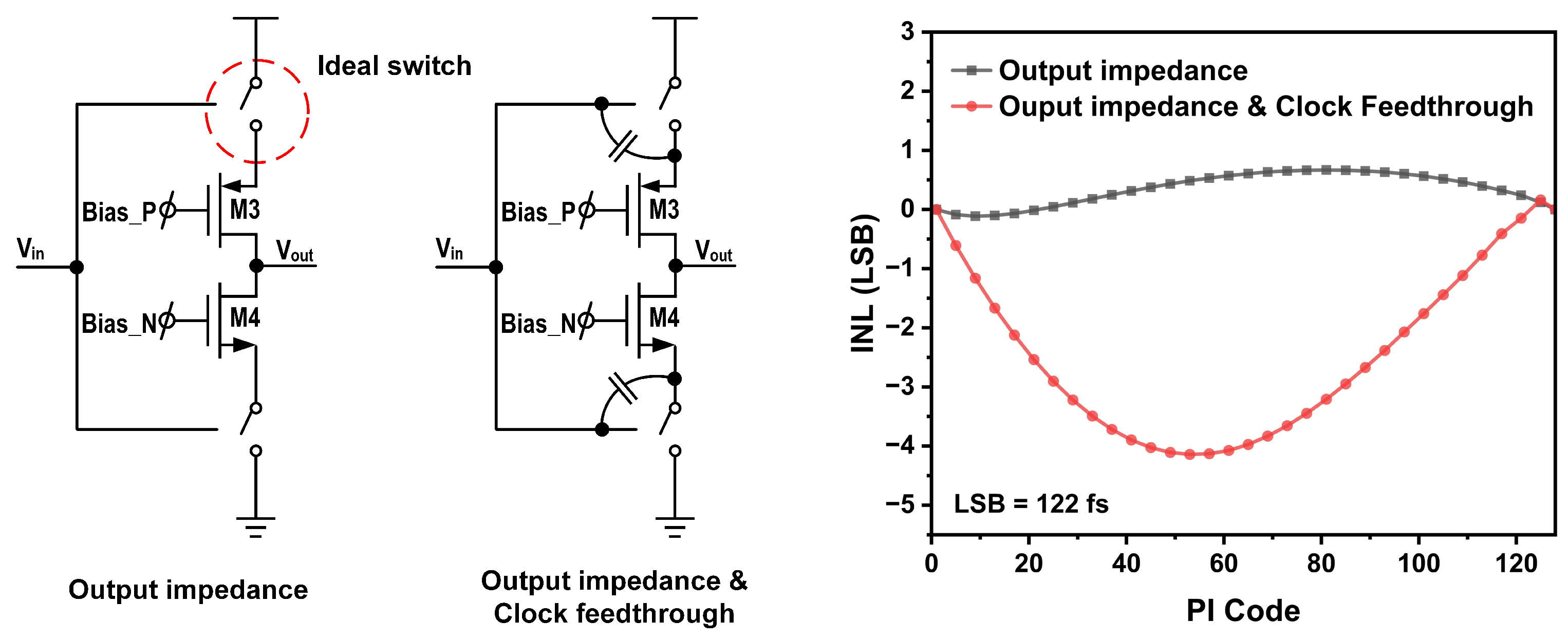
Having established the architecture and ideal operation of the proposed IMPI, this section provides a detailed analysis of the key non-idealities that degrade its linearity. To identify and decompose the dominant sources of nonlinearity, a specific transient simulation methodology was used, as illustrated in
Figure 4. The goal was to isolate nonlinearities from the current sources (M3/M4) versus the switches (M1/M2).
First, to isolate the “Output impedance” contribution, the real M1/M2 FinFET switches were replaced with ideal voltage-controlled switches (e.g., from the analogLib library) configured with near-zero on-resistance, infinite off-resistance, and zero parasitic capacitance. The INL was then simulated by sweeping the digital code M and measuring the output phase. The result, plotted as the “Output impedance” curve, isolates the INL contribution originating solely from the finite output impedance of the current sources (M3/M4).
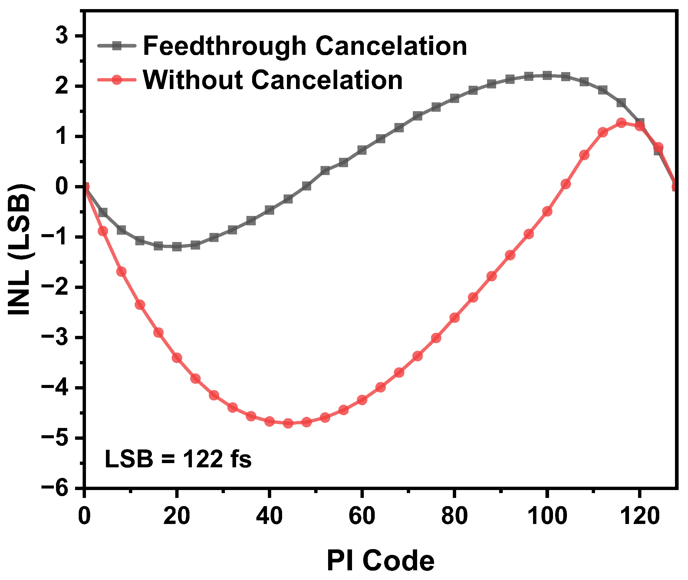
Next, to this same setup, ideal capacitors were added between the switch control input (clock) and the switch output node. These capacitors were sized to match the estimated gate-drain capacitance () of the original M1/M2 transistors. The INL simulation was repeated. The resulting “Output impedance & Clock Feedthrough” curve shows a dramatic increase in nonlinearity.
This comparative simulation clearly demonstrates that the asymmetrical clock feedthrough is the dominant source of nonlinearity in this architecture. The following subsections will provide a rigorous theoretical model for each of these key effects, with a primary focus on the clock feedthrough mechanism.
2.2.1. Modeling of Asymmetrical Clock Feedthrough
A comprehensive analysis reveals that the clock feedthrough nonlinearity is a composite effect. The physical mechanism is dynamic: taking a rising edge at the gate of the PMOS switch (M1) as an example, the feedthrough path evolves in two stages. In the initial phase of the transition, while M1 is still conductive, it provides a low-impedance path to VDD. Consequently, the majority of the current coupled through
, the gate-drain capacitance of M1, is shunted to the supply rail, having a minimal impact on the output. As the input voltage rises further and M1 enters the cutoff region, this shunting path disappears. The primary path for the feedthrough current now becomes the injection into the source of the current-source transistor, M3. It is this latter phase of the transition that is the dominant contributor to the nonlinearity. This two-stage mechanism underscores the sensitivity to the input slew rate; a slower edge, such as that of a sine wave, prolongs the duration of the harmful injection phase, leading to a larger total injected error charge.
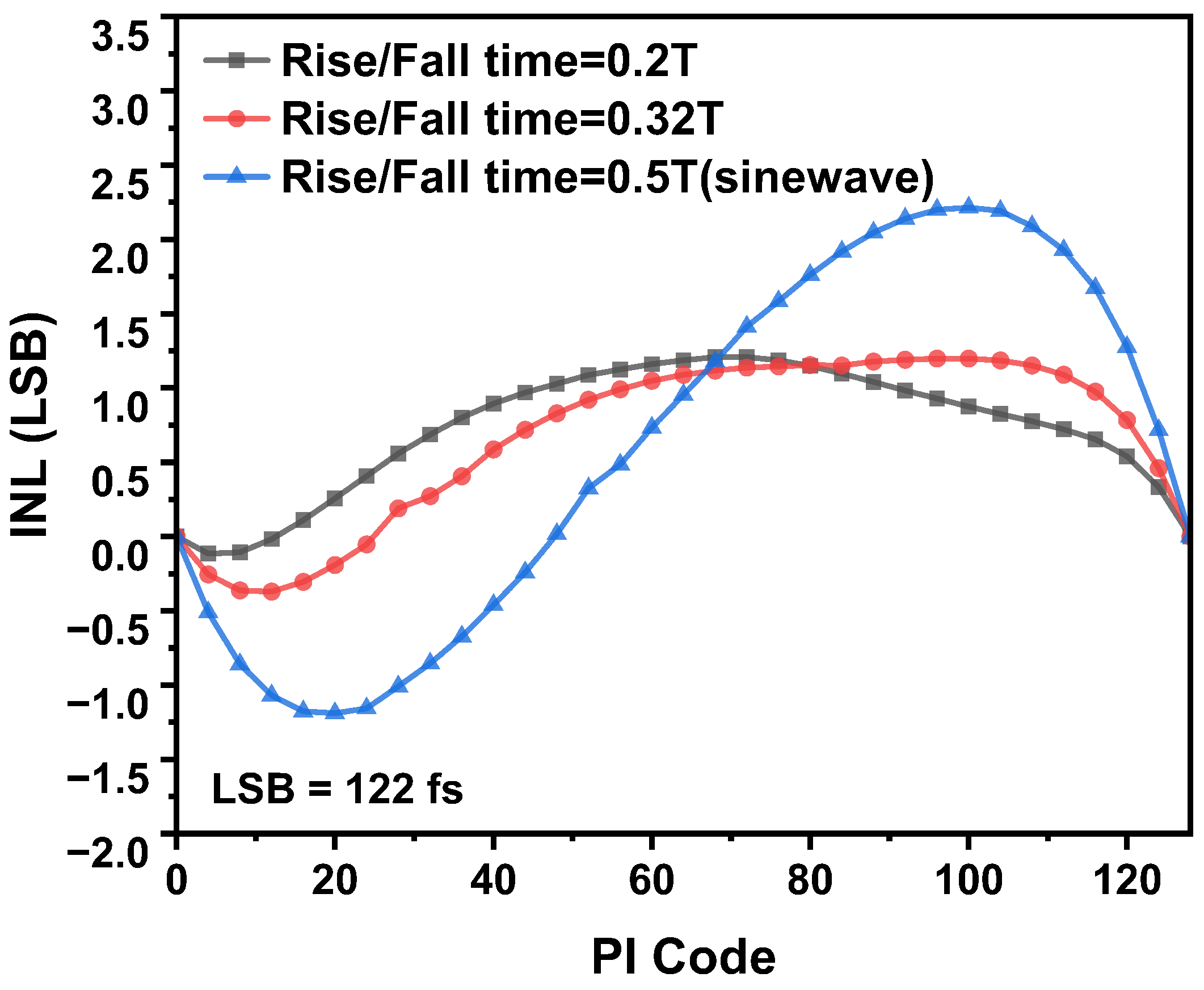
Figure 5 validates the model’s dependency on the input slew rate. The pre-layout simulation, run at 16 GHz (where the input clock period
ps), shows that sharpening the input edge from a pure sine-wave (0.5
T rise/fall time) to 0.2
T reduces the peak-to-peak INL by more than 50%, from approximately 3.5 LSB to 1.3 LSB. This result confirms the nonlinearity is fundamentally linked to the input transition duration, as predicted by our model.
This physical process can be modeled by considering the confluence of the code-dependent number of switching slices and the time-varying nature of the parasitic current. For a sinusoidal input
, the feedthrough current generated by a single PI slice,
, is proportional to the input’s slew rate. This can be modeled using an effective gate-drain capacitance,
. Here,
is an effective parameter that accounts for both the physical gate-drain capacitance of the switch and the “shielding effect” provided by the source impedance of the current-source transistors (M3/M4). This shielding can be understood by analyzing the feedthrough path when the switch (e.g., M1) is off. The physical
of the switch is effectively in series with the low source-impedance (approximately
) of the current-source transistor (M3). This series combination increases the total impedance of the feedthrough path. Therefore, the resulting feedthrough current
(and thus the total injected charge) is significantly reduced compared to a case where
would couple directly to the output node. The feedthrough current is thus given by:
where
is the input clock frequency and
is the power supply voltage (assume input clock is rail to rail). The charge injected by a single slice,
, is the integral of
over the code-dependent time window, resulting in:
In this design, the interpolation range spans one clock quadrant (
), where
T is the input clock period, which is divided into
N steps (e.g.,
). The time resolution per code, LSB, is thus defined as:
The integration duration,
, is then a direct linear function of the PI code
:
Crucially, the number of slices that are actively switching at the region transition is also determined by the PI code
M. The total injected charge,
, is the product of these two effects:
The resulting physical phase error,
, is proportional to this total injected charge. We can model the error term as:
where
and
is the integration current in the constant-slope region. This model starkly contrasts with the case of a square-wave input. For an idealized square-wave with a very fast slew rate, the two-stage injection process is completed within a very short, fixed time interval at the beginning of the clock transition. The resulting injected charge,
, becomes a constant value, independent of the subsequent integration time
and thus independent of the PI code
M. This code-independent charge injection manifests as a fixed DC offset on the output waveform, which does not degrade the PI’s integral nonlinearity. This complex, code-dependent nonlinearity therefore arises from two combined factors. The first is the continuous, time-varying slew rate of the sinusoidal input, and the second is the code-dependent integration window.
2.2.2. INL Formulation and Interpretation
The final INL observed in simulations is not the raw physical error, , but rather the form this error takes when subjected to the PI’s fundamental boundary conditions. This distinction is critical for correctly interpreting the results. The formulation can be understood in two steps:
First, we acknowledge the raw physical error source, , as modeled in the previous sections. This term represents the underlying nonlinearity from effects like clock feedthrough and has a non-zero value at the end of the range, .
Second, we must apply the system’s physical constraint. The PI is designed to interpolate between two fixed phase points (e.g., 0° and 90°). Therefore, regardless of any internal nonlinearities, the total accumulated phase at the end of the code range () must precisely equal the ideal total phase; i.e., . This implies that the net observable error at must be zero. To satisfy this boundary condition, the raw physical error, , must be inherently counteracted by a linear error component that represents a simple gain error of the overall transfer function. This linear correction term must be exactly equal to at the endpoint. Its form is therefore .
The final, observable INL is the superposition of the raw physical error and this system-level linear correction term. This leads to the final INL formula:
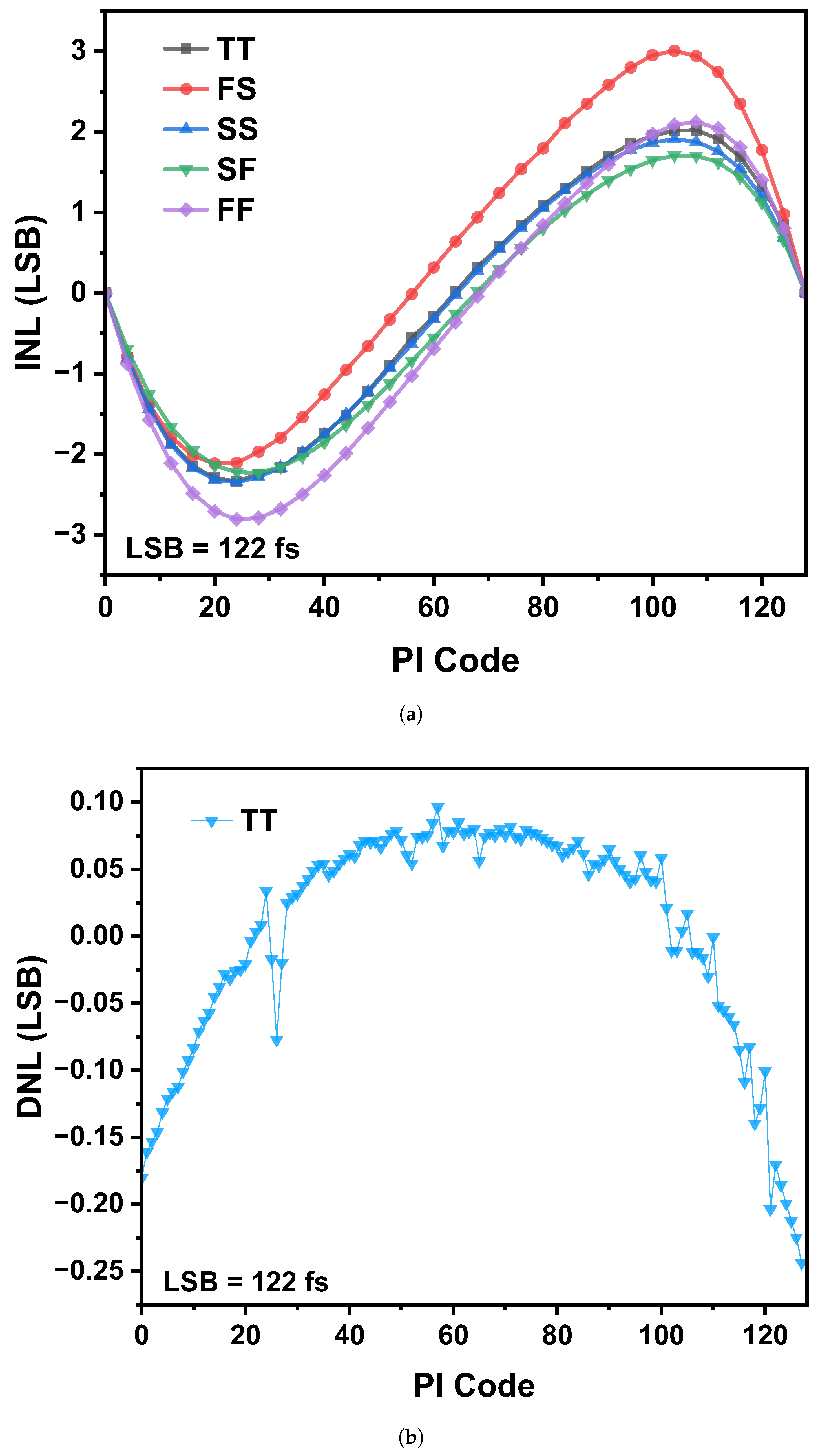
This physically derived formula is mathematically equivalent to the standard metrological definition of INL: the deviation of a transfer curve from a straight line drawn between its start and end points. This final equation explains the observed simulation results. The subtraction of the linear ramp term from the underlying physical error curve mathematically forces the INL at and to be zero and creates the characteristic arch-shaped or S-shaped INL curve.
2.2.3. Finite Output Impedance and Signal Swing Limitations
While the proposed architecture mitigates several sources of nonlinearity, its linearity is still fundamentally limited by the non-ideal characteristics of the current-source transistors (M3/M4). An ideal integrator requires a current source with infinite output impedance (). However, practical MOS transistors exhibit a finite that is also dependent on the output signal swing, which introduces timing errors. This section provides a detailed model of this effect.
First, we consider the current source as an ideal source
in parallel with a finite, but constant, output resistance
. This parallel resistance creates a path for current to leak from the load capacitor
, making the effective charging current dependent on the output voltage
. The behavior of this circuit is described by the following first-order differential equation, derived from Kirchhoff’s current law at the output node:
Solving this equation with the initial condition
, we find that the output voltage is not a linear ramp but an exponential function:
To quantify the deviation from an ideal linear ramp,
, we can use a Taylor series expansion for small
t:
The equation reveals a second-order error term that is proportional to and inversely proportional to . This term causes the voltage ramp to “droop” or bend downwards over time. Since the duration of the variable-slope integration phase, t, is determined by the PI’s digital code M, the accumulated voltage error at the end of this phase is a nonlinear function of the code. This code-dependent error directly translates into integral nonlinearity (INL).
The model above assumes a constant . In reality, the output impedance of the MOS current source varies significantly with its drain-source voltage (), which is directly related to the output voltage swing . This dependency is especially pronounced with large signal swings.
The output impedance is relatively high and stable only when the transistor is in the deep saturation region. However, as the output voltage swings towards the supply rails, the across the current-source transistor decreases. If the swing is excessively large, the saturation condition () is violated, and the transistor enters the triode region. In this region, the device no longer acts as a current source, and its output impedance drops drastically.
This sharp decline in at the extremes of the voltage swing means that the nonlinearity described by our model is significantly exacerbated at the beginning and end of the integration ramps. The error term proportional to becomes much larger, causing severe distortion of the triangular waveform and further degrading the PI’s linearity.
This detailed analysis provides direct theoretical justification for the design choices made in this work. To ensure high linearity, it is critical to both maximize the baseline and prevent the current-source transistors from entering the triode region. Therefore, a longer channel length of 36 nm is chosen to increase the intrinsic output impedance by mitigating channel length modulation. Simultaneously, the overdrive voltage is carefully optimized to be less than 0.1 V, which lowers the required saturation voltage () and maximizes the available linear signal swing before begins to drops drastically.
2.2.4. P/N Mismatch
In advanced FinFET processes, achieving precise matching between PMOS and NMOS devices is challenging due to the quantization of fin/gate dimensions. This inherent P/N mismatch is highly sensitive to process, voltage, and temperature (PVT) variations, leading to an imbalance between the pull-up and pull-down current networks.
For the IMPI to maintain a stable DC operating point over a full clock cycle, the net charge sourced to the output capacitor must equal the net charge sunk from it. If a P/N mismatch exists, the circuit will automatically seek a new equilibrium by shifting its output common-mode DC level. This shift alters the of the current-source transistors, modulating their currents via channel length modulation until the net charge is balanced to zero over one period.
The critical issue arises when a simple, fixed biasing scheme is used. Under significant PVT variations, the P/N mismatch can become severe, forcing the output DC level to shift substantially to maintain this charge balance. A large DC shift can dangerously reduce the available drain-source voltage for either the PMOS or NMOS current-source transistors. This can force the devices into the triode region, where they no longer behave as stable current sources but rather as low-impedance resistors. Operation in the triode region fundamentally violates the principle of linear integration, leading to severe nonlinearity.
Therefore, this analysis concludes that a fixed biasing strategy is not robust against PVT-induced P/N mismatch. It is essential to employ an adaptive biasing scheme that actively regulates the output DC level, ensuring the current-source transistors remain in the saturation region across all operating conditions.
2.2.5. Dynamic Errors from Asymmetrical Settling Time
Beyond static nonlinearities, dynamic errors arising from finite settling times are critical at 16 GHz. The core issue is the asymmetrical settling behavior at the internal parasitic nodes of the PI slices.
As an example, we analyze the transition from a variable-slope region (e.g., Region I) to a constant-slope region (e.g., Region II), where M of the N active NMOS switches must turn off. We focus on the internal node X, located between the NMOS switch (M2) and the current source (M4).
When M2 turns off, node
X loses its low-impedance path to ground. However, it is not immediately isolated; the output voltage
continues to drive a leakage current,
, through M4 into node
X. We make two key assumptions: (1) M2 provides a near-ideal discharge path when on, so the initial voltage is
; (2) The current source M4 follows a square-law model during this transient. The voltage at node
X thus follows:
where
is the parasitic capacitance at node
X,
is the initial overdrive voltage of M4, and
is its corresponding initial transconductance. Solving this yields:
The total error charge is the sum of charge accumulated on these nodes across all
M switching slices. Crucially, the leakage duration
t depends on the time the output ramp takes to cross the threshold, which is linearly related to the code:
. Substituting this into the solution yields:
For typical operation (
), this error approximates to a quadratic term (
). Finally, INL is defined after removing the ideal linear transfer function (zero-based end-point correction):
This mathematical form represents a symmetric, parabolic (arch-shaped) curve.
