1. Introduction
Electrification of the transportation sector plays a pivotal role in reducing the global carbon footprint. In this context, the sales of EVs exceeded 17 million globally in 2024, which corresponds to a share of more than 20%, while in 2025 it is expected that more than 20 million EVs will be sold [
1]. Therefore, the development of high-power EV charging infrastructure enabling simultaneous charging of multiple EVs becomes paramount to cater to the growing global EV market.
The impact of EV charging on the stable operation of distribution power grids and related concerns about power quality [
2] warrant the use of an advanced EV charging system. Such an advanced charging system should contain local energy storage to enhance the charging process and/or support the power grid. Energy storage can either be provided by a stationary battery storage system or through the EVs’ batteries, namely vehicle-to-grid (V2G) functionality.
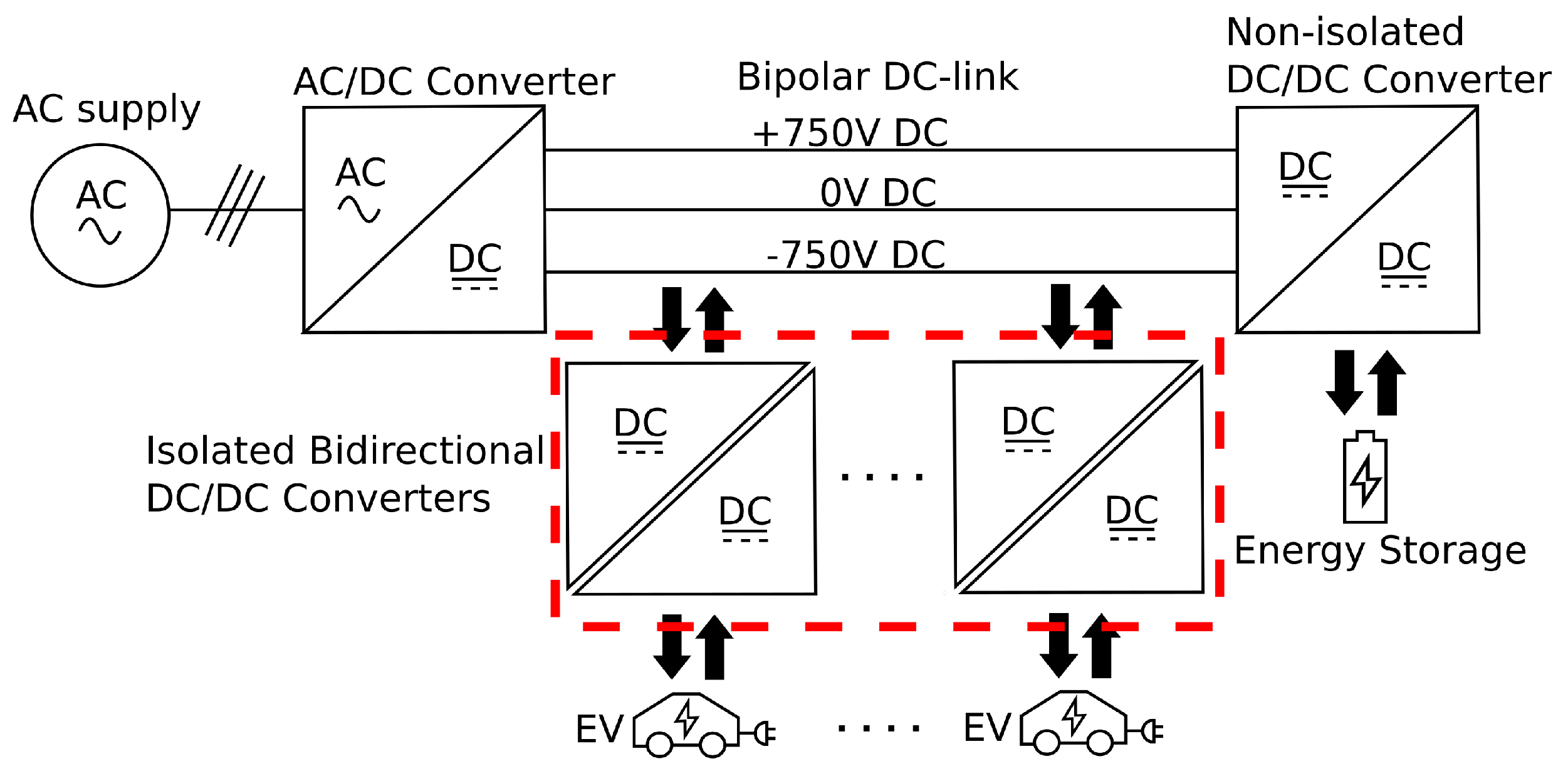
A block diagram of an advanced charging station is shown in
Figure 1.
One of the key steps in the development of such an EV charging system is to choose a relevant power electronics converter topology for the isolated bidirectional DC/DC converter (IBDC), which interfaces the EV charging system with the EVs. To enable V2G operation and also simultaneous charging operations of multiple EVs, the IBDC must be able to exhibit the best performance over a wide range of charging modes, e.g., slow charging, fast charging, and power flow towards the grid, and to comply with both 400 V and 800 V EVs’ battery systems. A solution to fulfill the entire spectrum of charging and grid support operations and comply with the various EVs’ battery voltages, without increasing the investments significantly, is to develop modularized and reconfigurable IBDCs. An optimal way to develop modularized and reconfigurable IBDCs is to deploy a large number of fundamental blocks with the same design in terms of circuit topology, components, and electrical ratings, which could be connected in parallel or series to reach the required charging voltage and power constraints. Deployment of a large number of fundamental blocks also provides fault redundancy in the event of failures and improves the fault tolerance capability of the EV charging system.
On this basis, the dual-active bridge (DAB) converter introduced in [
3] seems to be a suitable topological choice, taking into account its soft-switching capability, higher power density, galvanic isolation, bidirectional power flow capability, and wide voltage gain range [
4].
Silicon carbide (SiC) metal–oxide–semiconductor field-effect transistors (MOSFETs) have the capability to switch at higher frequencies, block higher voltages for the same conduction loss performance, and operate at higher temperatures compared to silicon (Si) insulated-gate bipolar transistors (IGBTs) [
5]. It has been shown that the use of SiC power devices in EV applications could be highly beneficial in terms of enhanced efficiency and compactness [
6,
7,
8]. Therefore, SiC-based DAB converters have been considered in this study. It has been shown that DAB-based IBDC topologies employing wide-band gap (WBG) power semiconductor devices enable a number of benefits in various applications, such as more electric aircrafts [
9], solid-state transformers (SST) [
10,
11], and EV charging [
12,
13].
A comprehensive comparison of both two-level and multi-level DAB-based IBDC topologies considering factors like efficiency, power density, cooling system, and electromagnetic interference (EMI) was presented in [
9]. However, only non-resonant DAB topologies were considered and they were not based on the same MOSFET technology; i.e., the primary bridge of each converter topology was either based on SiC MOSFETs or gallium nitride (GaN) high-electron-mobility transistors (HEMTs) and all the secondary bridges were based on silicon-based MOSFETs. In addition, the comparative evaluation has not been experimentally verified.
The authors in [
10] compared the performance of both non-resonant and resonant variants of conventional DAB converters based on half-bridge and full-bridge fundamental circuits using 5 kW experimental prototypes. However, the specifications of the employed SiC MOSFETs and the converter’s loss distribution were not analyzed.
A comparison of non-resonant and resonant versions of full-bridge-based DAB converters is presented in [
11]. The evaluated topologies were compared based on simulation and experimental results. However, the simulation modeling approach of SiC MOSFETs was not analyzed in detail. In addition, the experimental evaluation was not carried out fully on SiC-based prototypes, which makes the comparison unfair.
In [
12], a comparison between an interleaved buck converter (IBC) and DAB converter was conducted for a 350 kW rated charging system based on simulation studies. However, detailed loss analysis and experimental validation were not presented.
Taking into account the limitations of the above literature and considering the requirements of an EV charging system with a bipolar DC link, a first attempt to compare the performance of IBDCs was presented in [
13] by the authors.
The contribution of this paper is a thorough performance evaluation of six isolated bidirectional DC/DC converters employing SiC MOSFETs with the goal to identify the best-performing counterpart for designing a modularized and reconfigurable high-power EV charging system. The IBDCs under study are based on standardized designs of their primary and secondary circuits using discrete SiC MOSFETs, which enables a simplified and cost-effective design, softens maintenance, and, most importantly, allows for flexible and multiple parallel and series connections of the input and output stages of the IBDCs to serve various charging modes. The performance evaluation is based on a comprehensive theoretical analysis, electro-thermal modeling and simulations, and experimental validation under practical operating conditions in charging modes. The performance evaluation criteria are efficiency, required volt-ampere ratings of the SiC MOSFETs, and thermal behavior quantified through junction temperatures. The best-performing converter configuration, namely the series-resonant (SR) ISOP FB DAB converter, has been evaluated in bidirectional power flow mode and under a range of power and EV battery voltage values.
This article is organized as follows:
Section 2 provides a brief description of the off-board EV charging system considered for the comparative analysis of the IBDC configurations. In
Section 3, the background, choice and design considerations of the evaluated IBDC topologies are discussed. In
Section 4, the six IBDCs are compared based on SiC MOSFETs’ required volt-ampere ratings, loss, and thermal performance using theoretical analysis and electro-thermal simulations. A description of the experimental conditions and comparison of the IBDC prototypes based on the experimental results are presented in
Section 5. The bidirectional performance of the SR input-series output-parallel (ISOP) full-bridge (FB) DAB module is presented in
Section 6, considering a range of EV battery voltages.
Section 7 and
Section 8 present the discussion and conclusions, respectively.
2. Description of the EV Charging System with a Bipolar DC Link
Figure 1 depicts a block diagram of the advanced EV charging system considered in this article, an example of which was investigated in [
14]. The front-end AC/DC converter at the grid supply stage of the charging system transforms the three-phase AC voltage, supplied by the power grid, to a bipolar DC voltage, i.e., +750 V/0 V/−750 V. A DC link with a bipolar DC voltage is considered because it ensures lower on-state losses in devices, higher power quality, and enhanced flexibility [
15,
16,
17] while charging the EVs. The bipolar DC grid provides two different voltage levels: one that equals 1500 V between the positive and the negative poles and a second one of 750 V between the positive or negative pole and the neutral connector. Access to a bipolar DC grid facilitates the flexible connection of sources (e.g., photovoltaic, fuel cells, and battery energy storage) and loads (e.g., EV battery) with different voltage and power ratings to a single DC link. In addition, interfacing DC sources and loads with a DC grid reduces unnecessary AC/DC energy conversion stages compared to a conventional AC system, thus contributing towards lower power losses. Therefore, a bipolar DC grid is a relevant choice for an advanced EV charging system.
The considered front-end AC/DC converter is based on a three-level active neutral point clamped (ANPC) topology, as presented in [
18]. To achieve high efficiencies, each phase leg of the converter is constructed using the universal All-SiC MOSFET ANPC sub-module [
19].
A non-isolated DC/DC converter interfaces the bipolar DC link with the local battery energy storage. The energy storage increases the operation flexibility of the EV charging system as it can be used either independently (for example, during a grid fault) or in combination with the power grid (for example, when power demand increases during fast charging of EVs) to supply charging power to the EVs.
The EVs are interfaced with the DC link through multiple units of isolated bidirectional DC/DC converters (highlighted using red dashed box in
Figure 1), which are discussed in detail in
Section 3.
All the employed power converters are designed as bidirectional to facilitate various operating modes of the EV charging system, as described in [
14]. To ensure reconfigurability, modularity, easy maintenance, and repair of the considered EV charging system, all IBDC variants discussed in this paper are built with the same sub-modules. For example, in the case of the two-level DAB converter, the sub-module is the FB circuit used both on the primary and secondary sides. Furthermore, the sub-modules are designed using discrete power semiconductor devices that enable a simplified and cost-effective design.
The maximum power that can be supplied by the EV charging system is determined by the sum of the individual power ratings of the AC/DC converter (which processes the power from power grid) and the non-isolated DC/DC converter (which processes the power from the local battery energy storage), respectively. Each unit of IBDC can then be rated to smaller multiples of the maximum rated power of the charging system. In this article, the IBDC topologies have been evaluated at a rated power of 10 kW. The power ratings of the AC/DC converter and the local energy storage are not in the scope of this evaluation.
3. Description and Design Considerations of the Evaluated IBDC Topologies
In this section, an overview of the IBDC topologies evaluated in this article is presented. In addition, the rationale behind the choice of topology, design parameters, and the SiC MOSFETs used are explained.
3.1. Selection Criteria and Description of the IBDC Topologies
The salient features to be considered for the design evaluation of IBDC topologies, based on the application requirements, are summarized below:
Modularity and reconfigurability—(i) to provide flexibility in terms of supplied output voltage and charging power by appropriate interconnections of multiple modules, (ii) to reduce maintenance and repair efforts (i.e., easily replaceable), and (iii) to reduce system complexity (i.e., plug and play).
Bidirectionality—to ensure grid-to-vehicle (G2V) and vehicle-to-grid (V2G) operations.
Galvanic isolation—to comply with the functional requirement of the IEC 61851-23:2014 standard [
20] and to provide protection to the EVs during system faults (for example, a short-circuit fault in the DC link).
The DAB converter topology shown in
Figure 2 incorporates all of the above-listed features and, therefore, appears to be the most suitable topology for the EV charging system considered.
A DAB converter consists of two active bridges, conventionally two FB circuits, that are galvanically isolated by a high-frequency transformer. The converter can be operated in either the buck or boost mode depending on the transformer turn ratio. The two active bridges (in this case FBs) can be manufactured based on the same sub-module design, thereby ensuring modularity. The voltage and current ratings of the discrete MOSFETs in the individual active bridges can be chosen based on the type of DC voltage source (e.g., DC link and EV battery) to which it is connected, ensuring flexibility.
In the positive power flow direction, the primary FB operates as an inverter and the secondary FB as a rectifier. In the commonly employed single-phase-shift (SPS) modulation of DAB, the switches in both the FBs are switched at a 50% fixed duty ratio to generate high-frequency AC square-wave voltages across the transformer’s primary and secondary sides. The series inductance,
L, in
Figure 2 represents the sum of the high-frequency transformer’s leakage inductance and any parasitic and/or external inductance in the circuit. This series inductance introduces a phase difference between the primary and secondary FB voltages, which can be adjusted to control the magnitude and direction of the transferred power (similarly to conventional AC power systems). Therefore, bidirectional power flow (i.e., from the bipolar DC grid to the EV and EV to the DC grid) can be achieved.
Considering the two-terminal nature of the EV battery load and the bipolar (three-wire) nature of the DC link in the EV charging system (see
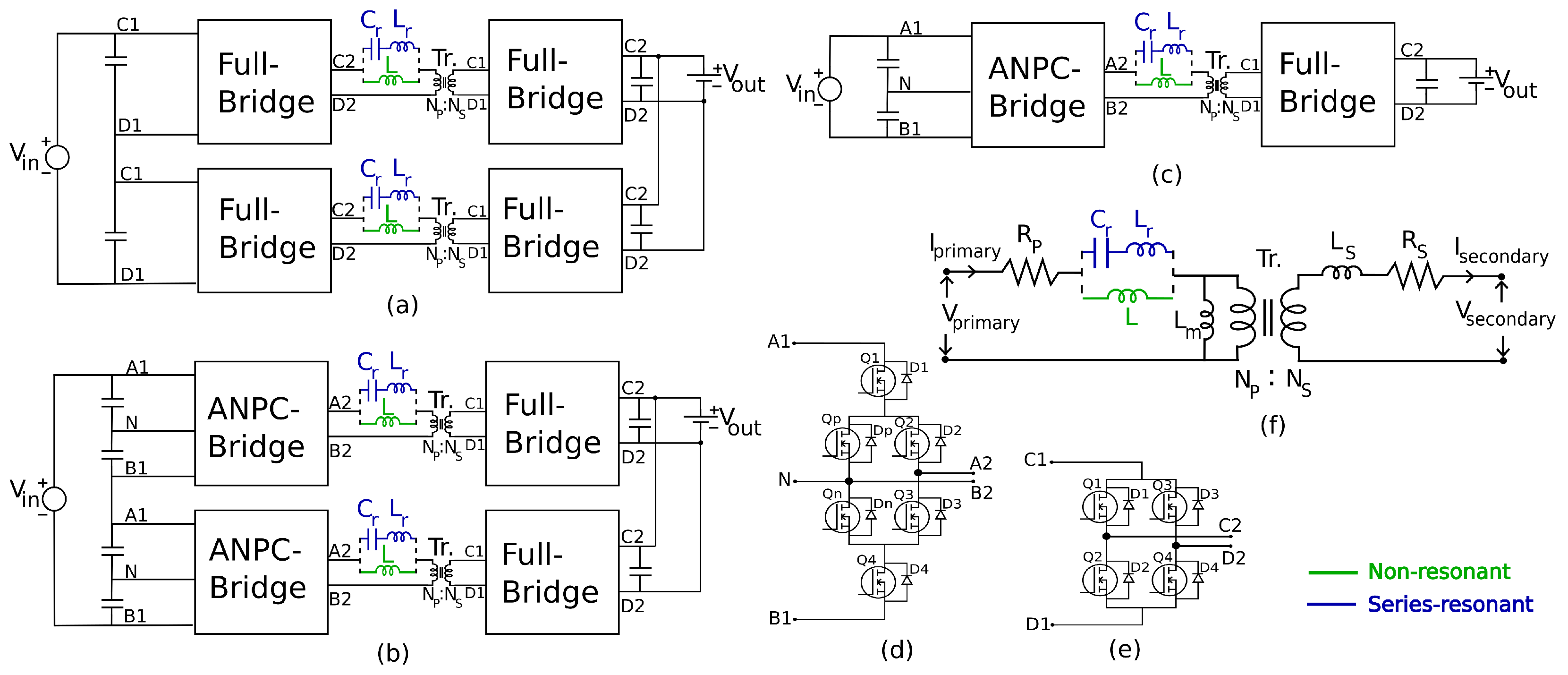
Figure 1), two fundamental circuits, namely, the full-bridge (FB) and the active neutral point clamped (ANPC) circuits (
Figure 3d,e), have been identified to be used as active bridges in the DAB-based IBDC topologies depicted in
Figure 3a–c.
Three options for interfacing the primary active bridge with the three-wire DC link have been considered for evaluation: (i) through series-connected FB circuits in
Figure 3a, (ii) through series-connected ANPC circuits in
Figure 3b, and (iii) through a single ANPC bridge in
Figure 3c. The secondary active bridge, in all of the evaluated IBDC topologies, is based on the FB circuit, since the load is the two-terminal EV battery.
The ISOP configuration employed in the modular topologies, shown in
Figure 3a,b, provides voltage flexibility on the primary side through series-connected circuits and power scalability on the secondary side through parallel-connected circuits. For the same transferred power, the ANPC DAB topology shown in
Figure 3c utilizes half the number of SiC MOSFETs compared to the ISOP ANPC DAB (
Figure 3b). However, the voltage rating of the SiC MOSFETs used in the primary ANPC bridge of the ANPC DAB is double that of the SiC MOSFETs used in each primary ANPC bridge of the ISOP ANPC DAB.
Both series-resonant (SR) and non-resonant (NR) variants of each of the three listed topologies were evaluated to study their performance, as well as advantages and disadvantages. Topologically, the SR DAB configurations require an additional capacitor to form an
resonant tank (shown in blue in
Figure 3a–c) compared to the NR DAB converters, which only have a series inductance, L (shown in green in
Figure 3a–c).
3.2. Design Considerations
The selected topologies depicted in
Figure 3 were evaluated under the same voltage and power levels.
Table 1 summarizes the chosen SiC MOSFETs for the non-resonant and series-resonant versions of each topology and their respective ratings (see footnotes 1, 2, and 3).
The values considered for the DC input voltage (
), DC output voltage (
), power transferred (
P), switching frequency (
), magnetizing inductance of transformer (
), equivalent primary DC resistance (
), equivalent secondary DC resistance (
), dead time (
), thermal resistance of heatsink for each active bridge (
), resonant frequency (
), resonant series inductance (
), resonant capacitance (
), non-resonant series inductance (
L), and transformer turn ratio (
N) are summarized in
Table 2.
It should be noted that N is the ratio of the number of transformer primary turns to the number of transformer secondary turns. N is chosen to be equal to the ratio of the transformer terminal voltages to achieve a unity voltage transfer ratio. The reason for this is to maximize the zero voltage switching (ZVS) range and to reduce the stress on the transformer by reducing circulating currents.
The selection of SiC MOSFETs was made considering devices encapsulated in discrete packages, the type of bridge circuit (i.e., ANPC or FB), the considered voltage and power levels of the ANPC and FB modules, better switching performance in terms of faster switching transients due to lower stray inductance in the gate loop (four-pin devices with Kelvin connection), and their availability in the market.
The switching frequency,
, was chosen to be 100 kHz as a fair trade-off between the heatsink size, the size of magnetics, and the switching losses. The thermal resistance was determined based on the data sheet of the LA6/150/24 V aluminium extruded heatsink from Fischer elektronik [
21]. Since performance evaluations based on efficiency and losses of SiC MOSFETs are carried out at a specific operating point, the EV battery is modeled as a constant DC voltage source.
The power transfer equation for a non-resonant DAB converter operating with SPS modulation is given by
where D is the phase-shift ratio (0 < D < 1) between the primary and the secondary active bridge. The non-resonant series-inductance,
L, is calculated according to Equation (
1) for a phase shift of D = 0.5 and for twice the nominal power level. The reason for this approach is to ensure lower reflow power at the nominal operating point. Reflow power refers to the power flow back to the source caused by circulating currents in the converter, thus causing additional power losses and resulting in an efficiency drop [
22].
It should be noted that the value of L is calculated at P = 10 kW per each module of the ISOP FB DAB and ISOP ANPC DAB configurations (each module is operated at 5 kW nominal power) and at P = 20 kW for the ANPC DAB configuration for a nominal operating power of P = 10 kW. Therefore, the rated power transfer from the bipolar DC link through any of the considered topologies equals 10 kW.
In the case of resonant DABs, the
and
values are chosen such that the resonance frequency
is less than the switching frequency
of the converter to ensure continuous current mode operation [
23]. The resonance frequency,
, is given by
5. Experimental Evaluation of IBDC Topologies
This section first presents a description of the experimental prototypes and design parameters of the evaluated topologies. Furthermore, a comparison of the electrical performance of the IBDC topologies is presented based on experimental measurements of the transformer’s primary and secondary voltage and current waveforms. Finally, the IBDC configurations are compared based on power losses and efficiency measurements and estimations.
5.1. Description of Experiments
Full-scale prototypes of all six IBDC configurations depicted in
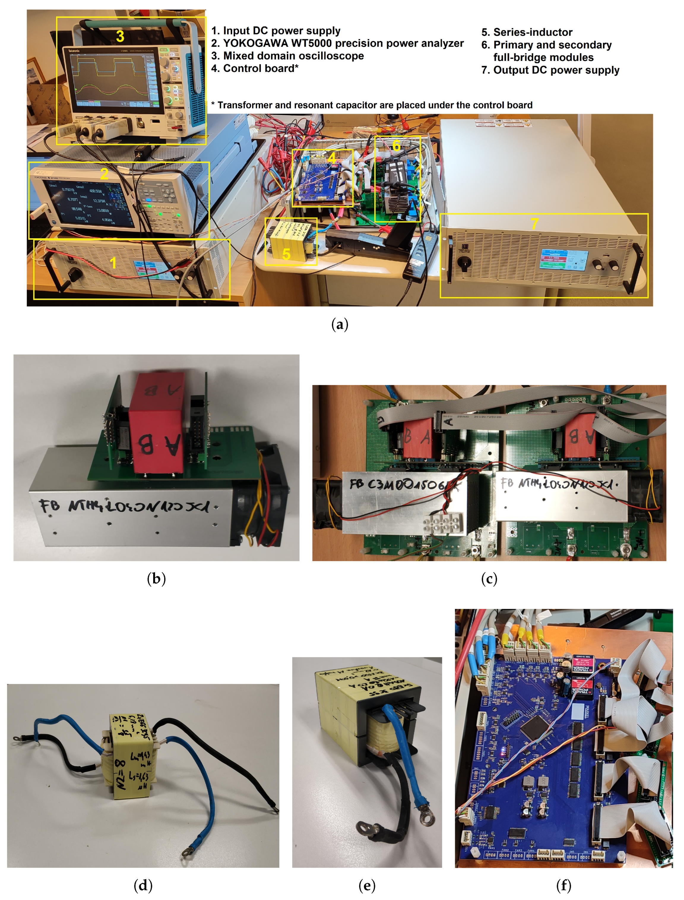
Figure 3 were developed and tested. The experimental setup of one of the six IBDCs, namely the series-resonant ISOP FB DAB, is shown in
Figure 6.
Presuming that the two parallel-connected DAB modules share the total power transferred in an ISOP DAB configuration, validation of a single DAB module should be sufficient in terms of assessing efficiency and loss performance. Therefore, 5 kW prototypes of single modules of non-resonant and series-resonant variants of ISOP-based IBDCs were used for the experimental validation. This is reflected in the design parameters and operating conditions summarized in
Table 4.
In this table, the equivalent primary DC resistance, , represents the sum of the DC resistances of the series inductor’s winding and transformer’s primary winding, while the equivalent secondary DC resistance, , corresponds to the DC resistance of the transformer’s secondary winding.
The values of non-resonant and resonant series inductances,
L and
, respectively, in
Table 4 represent the sum of the series inductor’s inductance and the transformer’s leakage inductance on the primary side. The secondary series inductance,
, corresponds to the transformer’s leakage inductance on the secondary side.
For the NR and SR variants of ISOP ANPC DABs, the practically achieved value of the transformer turn ratio, N, was 0.9091 (10:11) (see
Table 4), as opposed to the designed value of 0.9375 (15:16) (see
Table 2). For all other IBDC topologies evaluated, the designed value of N (i.e., 15:8) was practically achieved.
The EA-PSBE 12000-40 and EA-PSB 11000-80 bidirectional DC power supplies from EA Elektro-Automatik (Viersen, Germany) were used to supply the input and output voltages of the IBDC prototypes, respectively. The transformer’s primary and secondary voltages were measured using Tektronix’s (Beaverton, OR, USA) THDP0200 high-voltage differential probes. The primary and secondary currents of the transformer were measured using Tektronix’s TCP0150 and TCP303 current probes. A Tektronix 3 series MDO34 mixed-domain oscilloscope was used to observe the measurements for all the IBDC configurations.
The efficiency measurements were carried out using the WT5000 precision power analyzer from Yokogawa Electric (Tokyo, Japan), which has a basic power accuracy of ±0.03%. The DC power accuracy is 0.02% of reading +0.05% of range and the accuracy specifications are guaranteed from 1% to 130% of the selected voltage and current ranges [
30].
5.2. Observations and Comparison Based on Transformer’s Voltage and Current Waveforms
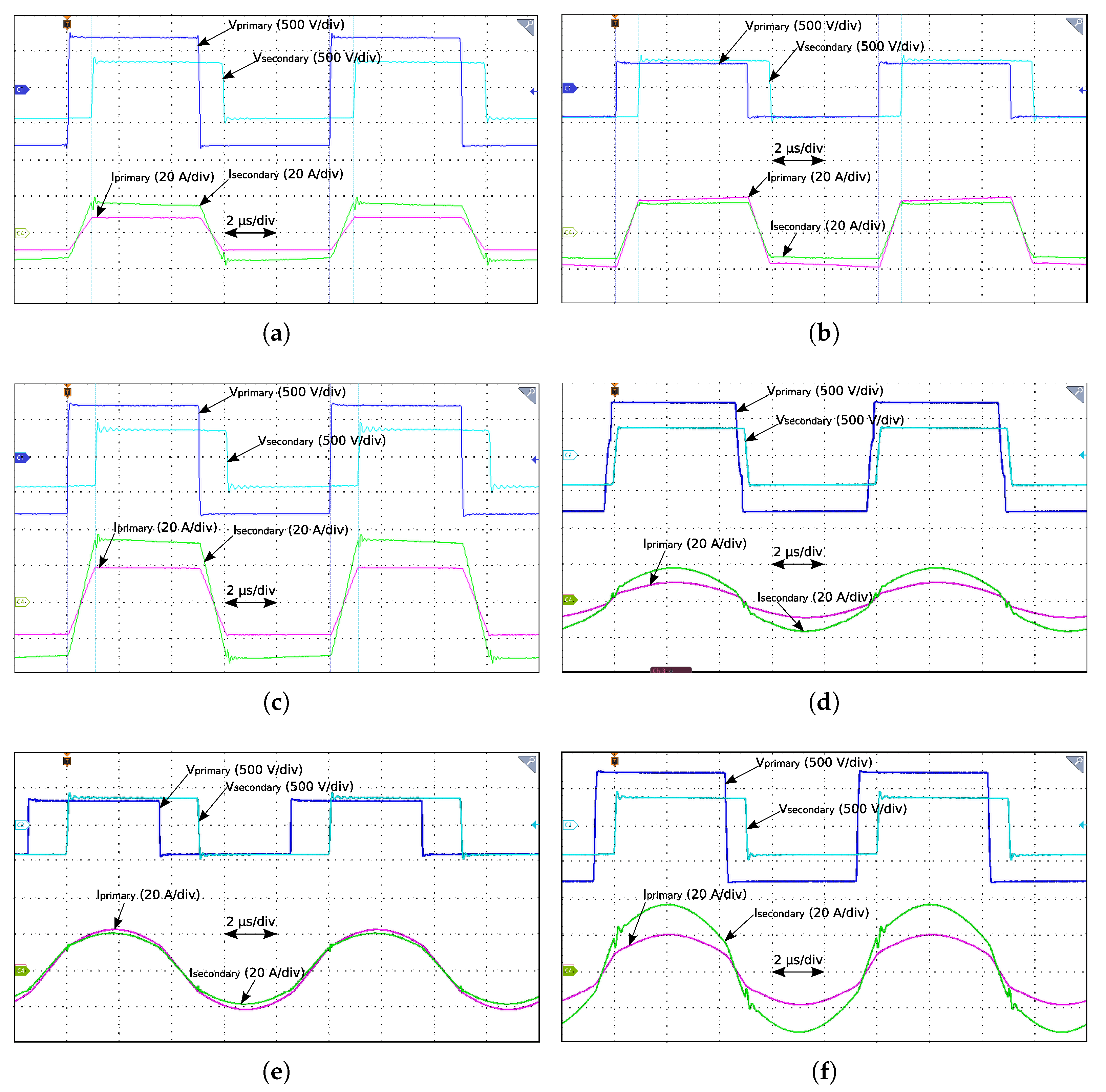
The voltage and current waveforms measured at the transformer’s primary and secondary sides are shown in
Figure 7a–f for the six investigated topologies.
Most of the observations regarding SiC MOSFET loss distribution, discussed in
Section 4.2, can be validated from the experimental waveforms in
Figure 7. From
Figure 7d–f, it can be observed that the SR IBDC configurations have a near-sinusoidal transformer current waveform compared to the trapezoidal current waveform of their non-resonant counterparts (
Figure 7a–c), resulting in lower RMS current values and thus lower conduction power losses.
Considering the NR and SR variants of the ISOP FB DAB (
Figure 7a,d) and ISOP ANPC DAB (
Figure 7b,e), respectively, it can be observed that the peak transformer primary currents in the NR ISOP ANPC DAB (nearly 20 A) and SR ISOP ANPC DAB (nearly 22.5 A) are more than double when compared to those of the NR ISOP FB DAB (nearly 9.4 A) and the SR ISOP FB DAB (nearly 9.8 A). In addition, the ISOP ANPC DABs reflect half of the DC input voltage on the transformer primary (375 V) compared to ISOP FB DABs (750 V) for the same power transferred (i.e., 5 kW).
Considering the corresponding RMS values of the transformer primary currents (
) in ISOP-based DAB topologies from
Table 5, the primary bridge conduction losses in NR and SR ISOP ANPC DABs will be more than four times higher (since conduction loss is proportional to square of the RMS value of current) compared to the respective ISOP FB DAB counterparts. This relation between the primary bridge conduction losses can be seen in
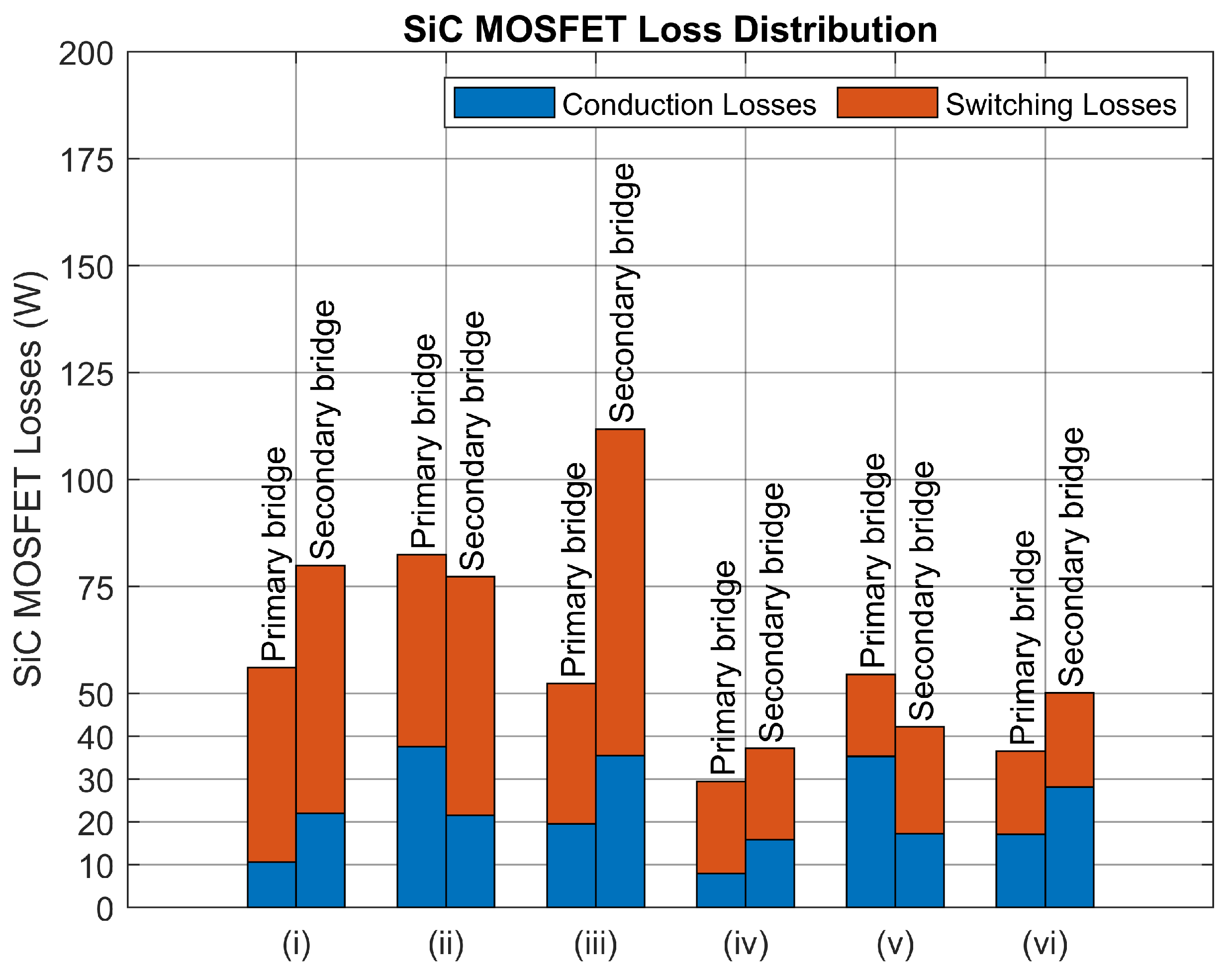
Figure 4i,ii,iv,v.
From
Figure 7b,c,e,f it can be seen that even though the NR and SR ANPC DABs transfer twice the power (i.e., 10 kW) when compared to the single modules of NR and SR ISOP ANPC DABs (i.e., 5 kW), respectively, their peak transformer primary currents are almost the same. Taking into account their corresponding RMS values from
Table 5, the primary bridge conduction losses for NR and SR ISOP ANPC DABs will almost be double those of the NR and SR ANPC DABs, respectively, for
P = 10 kW. This validates the relation between the primary conduction losses shown in
Figure 4ii,iii,v,vi.
Considering the operation of a full bridge (see
Figure 3e) under the SPS modulation scheme, switches Q1 and Q4 conduct to generate a positive bridge voltage, while switches Q2 and Q3 conduct to generate a negative bridge voltage. So each time the bridge voltage polarity changes, two MOSFETs are turned on and two MOSFETs are turned off. From the discussion in
Section 4.2, the main contributor to switching losses is the MOSFET turn-off losses. Therefore, the magnitude of the current at which the MOSFETs turn off becomes significant.
From the secondary bridge voltage (cyan) and current (green) waveforms in
Figure 7c, it can be observed that the secondary bridge MOSFETs in NR ANPC DAB turn off at peak current values. This validates the observation from
Figure 4iii in
Section 4.2 that the NR ANPC DAB has the highest secondary bridge switching loss. Similarly, the near-zero current switching in both primary and secondary bridges of the SR ISOP FB DAB can be observed in
Figure 7d.
5.3. Comparison Based on Non-MOSFET Losses
The losses incurred in the series inductor, transformer, equivalent series resistance (ESR) of the resonant capacitor, and resistive voltage divider (used for measuring
and
) are categorized as non-MOSFET losses and are listed in
Table 5 for all the evaluated IBDC configurations.
Table 5.
Transformer’s primary () and secondary () RMS currents and losses from passive components and voltage dividers. Note: The values in brackets correspond to losses computed for two ISOP DAB modules, each operating at P = 5 kW.
Table 5.
Transformer’s primary () and secondary () RMS currents and losses from passive components and voltage dividers. Note: The values in brackets correspond to losses computed for two ISOP DAB modules, each operating at P = 5 kW.
| Parameter | NR ISOP FB DAB | NR ISOP ANPC DAB | NR ANPC DAB | SR ISOP FB DAB | SR ISOP ANPC DAB | SR ANPC DAB |
|---|
| (Figure 3a) | (Figure 3b) | (Figure 3c) | (Figure 3a) | (Figure 3b) | (Figure 3c) |
|---|
| (A) | 8.42 | 17.19 | 17.16 | 7.25 | 16.55 | 14.75 |
| (A) | 14.46 | 14.36 | 29.91 | 13.16 | 14.87 | 26.96 |
| Inductor losses (W) | 2.05 (4.10) | 3.69 (7.38) | 8.23 | 2.50 (5.00) | 17.95 (35.90) | 13.99 |
| Transformer losses (W) | 2.29 (4.58) | 2.26 (4.52) | 9.49 | 1.87 (3.74) | 2.27 (4.54) | 7.55 |
| Losses from ESR of (W) | 0 | 0 | 0 | 0.53 (1.06) | 2.76 (5.52) | 2.19 |
| Voltage divider losses (W) | 7.72 (15.44) | 7.72 (15.44) | 18.88 | 7.72 (15.44) | 7.72 (15.44) | 18.88 |
| Total non-MOSFET losses (W) | 12.06 (24.12) | 13.67 (27.34) | 36.60 | 12.62 (25.24) | 30.70 (61.40) | 42.61 |
The winding losses,
, in the series inductor and transformer were calculated using Equation (
3):
where
is the RMS current flowing through a particular winding and
is the DC resistance of the corresponding winding. Since the focus is on understanding the relative differences in winding losses between the evaluated topologies, the AC resistance of the winding, taking into account the skin and proximity effects, was not calculated. This simplifies the winding loss calculation. However, the effect of the actual magnetic losses is reflected in the experimental efficiencies presented in
Figure 8.
The core losses,
, in the series inductor and transformer were calculated using Equation (
4):
where
is the power loss per unit volume of the core. This value can be obtained from the
vs. peak magnetic flux density plot in the core material’s data sheet for a particular switching frequency (100 kHz in this case).
The peak magnetic flux densities in the non-resonant/resonant series inductor (
), non-resonant IBDC transformer (
), and series-resonant IBDC transformer (
) were calculated using Equations (
5), (
6) and (
7), respectively.
where
L is the inductance of the non-resonant/resonant series inductor,
is the peak value of the series inductor current,
n is the number of turns (number of primary turns in the case of the transformer),
is the effective core area,
is the phase-shift angle between the primary and secondary active bridges,
is the peak value of the transformer primary voltage, and
and
are the peak values of the transformer primary current in the series-resonant and non-resonant IBDCs, respectively.
Losses incurred in the ESR of the resonant capacitor,
, were calculated using Equation (
8):
where the ESR of the resonant capacitor was measured at a switching frequency of 100 kHz using an E4990A impedance analyzer from Keysight (Santa Rosa, CA, USA).
Losses in the resistive voltage divider,
, were calculated using Equation (
9):
where
refers to the input or output DC voltage and
is the equivalent resistance of the resistor divider on the primary (151.2 k
) or secondary (40 k
) active bridge.
For a power transfer of
P = 10 kW, the total non-MOSFET losses are the highest for the SR ISOP ANPC configuration, as seen from
Table 5. The major reason for this is higher losses in the resonant series inductor. Considering Equation (
5), the product of
is the highest for the SR ISOP ANPC topology. This results in a high peak magnetic flux density and consequently the highest inductor core losses compared to other IBDC topologies.
The NR ISOP FB DAB topology exhibits the lowest non-MOSFET losses, followed by its series-resonant counterpart, i.e., SR ISOP FB DAB, which is not far behind.
5.4. Comparison Based on SiC MOSFETs’ VA Ratings Considering Individual IBDC Ratings
The comparison of IBDCs based on SiC MOSFETs’ VA ratings, presented in
Section 4.1, gives an indication of the IBDC prototypes’ costs depending on the chosen SiC MOSFETs’ ratings. However, a better performance indicator would be to consider the actual operating conditions of the SiC MOSFETs, in terms of voltage and current, in the individual IBDC topologies.
Therefore,
Table 6 presents a comparison of the SiC MOSFETs’ VA ratings estimated based on the VA ratings required by the respective active bridges of each IBDC configuration. The VA ratings are calculated as a product of the total number of SiC MOSFETs per primary or secondary active bridge, the IBDC transformer’s primary or secondary voltage, and the IBDC transformer’s primary or secondary RMS current (listed in
Table 5).
It can be inferred from
Table 6 that the NR ANPC DAB requires the maximum VA ratings of SiC MOSFETs, although NR and SR ISOP ANPC DABs are not far behind. The SR ISOP FB DAB requires the lowest VA ratings of SiC MOSFETs and is the clear winner based on this evaluation criterion.
5.5. Comparison Based on Efficiency Trend
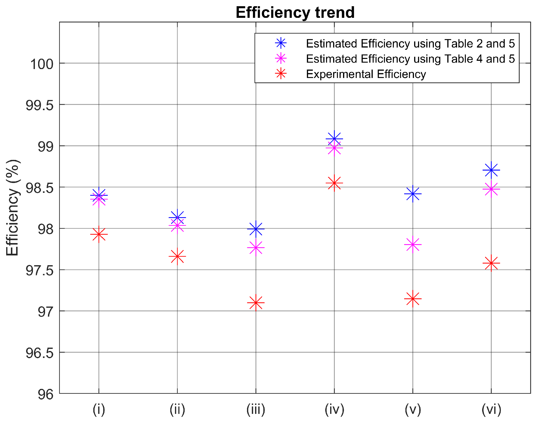
The trend in the estimated and experimental efficiency values for the six IBDC configurations is shown in
Figure 8. The estimated efficiencies take into account two loss components: (i) total SiC MOSFET losses obtained from electro-thermal simulations in PLECS by either considering the assumed design parameters in
Table 2 (in case of blue asterisks in
Figure 8) or by considering the actual experimental parameters in
Table 4 (in case of magenta asterisks in
Figure 8) and (ii) the sum of the non-MOSFET losses given in
Table 5.
Figure 8.
Efficiency trend: Estimated and experimental efficiencies of (i) NR ISOP FB DAB, (ii) NR ISOP ANPC DAB, (iii) NR ANPC DAB, (iv) SR ISOP FB DAB, (v) SR ISOP ANPC DAB, and (vi) SR ANPC DAB.
Figure 8.
Efficiency trend: Estimated and experimental efficiencies of (i) NR ISOP FB DAB, (ii) NR ISOP ANPC DAB, (iii) NR ANPC DAB, (iv) SR ISOP FB DAB, (v) SR ISOP ANPC DAB, and (vi) SR ANPC DAB.
From
Figure 8v, it can be observed that the estimated efficiency using
Table 4 and
Table 5 (magenta asterisks) for the SR ISOP ANPC DAB topology is significantly lower compared to the estimated efficiency using
Table 2 and
Table 5 (blue asterisks). The practically achieved value of the transformer turn ratio, N, was 0.9091 (10:11) (see
Table 4), as opposed to the designed value of 0.9375 (15:16) (see
Table 2). This results in higher MOSFET losses due to increased peak and RMS values of bridge currents, which causes the difference between the two estimated efficiencies.
In general, the experimentally obtained efficiency trend (red asterisks in
Figure 8) agrees with the efficiency trend based on values estimated using
Table 4 and
Table 5 (magenta asterisks in
Figure 8). It can be observed that the difference between them, for each topology, is nearly proportional to the RMS values of the respective transformer secondary currents (
) given in
Table 5.
Therefore, the reason for the difference can be mainly attributed to ignorance of skin and proximity effects (i.e., AC resistance) in the calculation of winding losses, non-consideration of contact resistances in the circuit, simulation-based estimation of MOSFET losses, etc.
The highest experimental efficiency value of 98.55% was obtained for the SR ISOP FB DAB, while the NR ANPC DAB recorded the lowest value of 97.1% for the considered operating conditions. Therefore, the SR ISOP FB DAB configuration will be used in assessing the bidirectional performance.
6. Bidirectional Performance of the SR ISOP FB DAB Considering a Range of EV Battery Voltages
To analyze an IBDC for a bidirectional off-board EV charging system, it is important to understand its operating performance at different power and EV battery voltage values in both directions of power flow, i.e., DC link to EV and EV to DC link. Since the SR ISOP FB DAB has been shown to be the best topology in terms of efficiency, the experimental efficiencies of a single module of an SR ISOP FB DAB are presented in this section.
A power range of 1–5 kW and an EV battery voltage range of 325–425 V have been considered. The voltage range is chosen to emulate the voltage ratings of real EVs such as Audi eTron and Jaguar iPace, which have a nominal operating voltage of approximately 400 V.
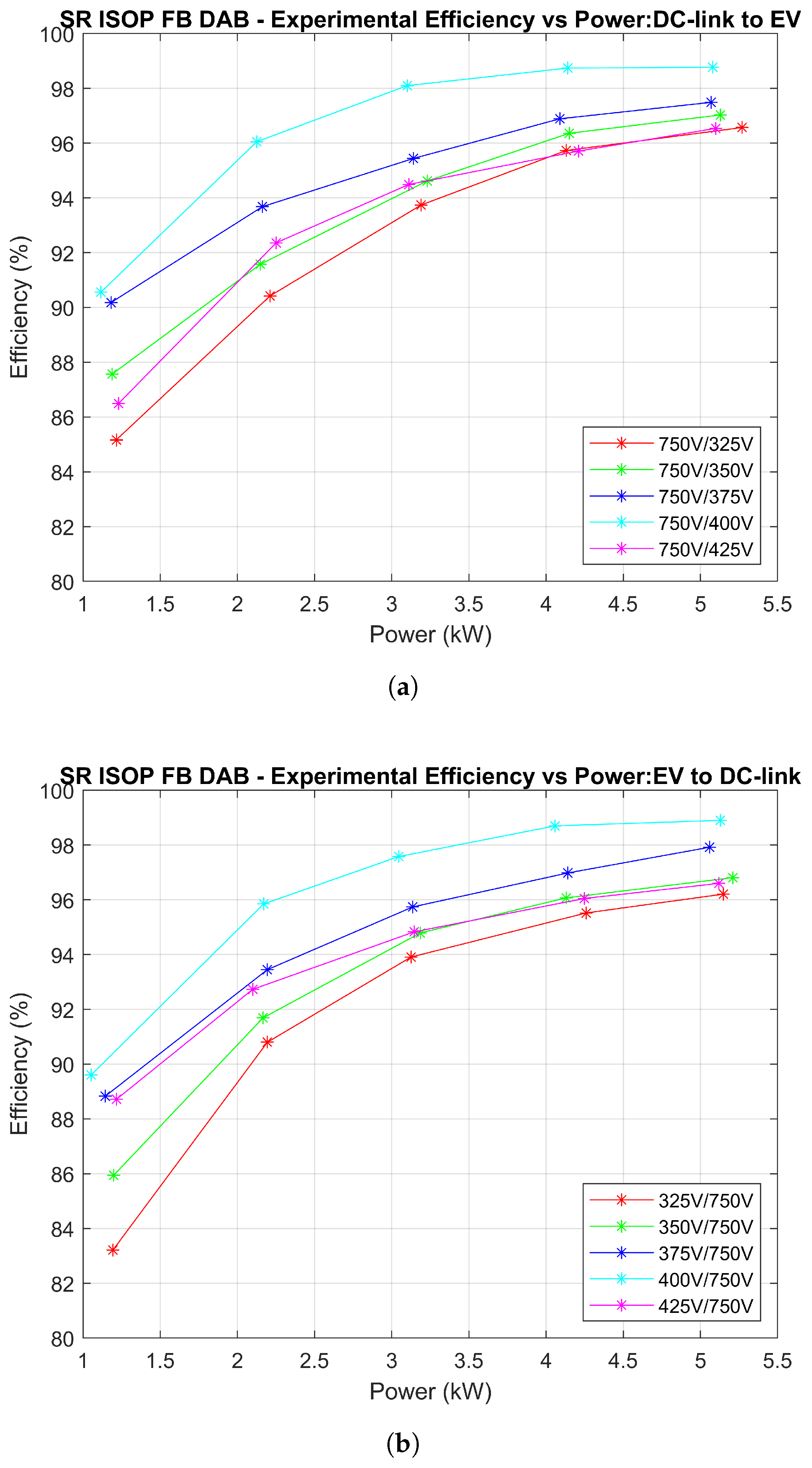
The measured efficiency results for both directions of power flow are shown in
Figure 9, where
Figure 9a considers the power flow from the DC link to the EV battery and
Figure 9b considers the power flow from the EV battery to the DC link.
Since a single module of the SR ISOP FB DAB converter is designed for a nominal DC link voltage of 750 V and a nominal EV voltage of 400 V, the maximum efficiency is achieved at this operating point. It should be noted that the SR ISOP FB DAB is designed for a maximum rated power of 10 kW and the peak efficiency occurs at around half the rated value, i.e., at a nominal operating power of 5 kW. This is true for both directions of power flow, as seen in
Figure 9a,b.
It can be observed from
Figure 9a,b that a decrease in operating power below 2 kW results in a significant reduction in the converter’s efficiency. Above 2 kW, there is no notable difference between the efficiency curves in both forward and reverse power flow directions. A good operating range for the converter in terms of power, considering an EV battery voltage range of 325–425 V, is between 3 and 5 kW to achieve an efficiency above 94%.
In a high-power EV charging station with multiple IBDC modules, the power rating of the individual module that results in the highest efficiency (over a wide range of EV battery voltages in both charging directions) is decisive for determining the total number of parallel-connected modules needed to achieve a specific charging power.
7. Discussion
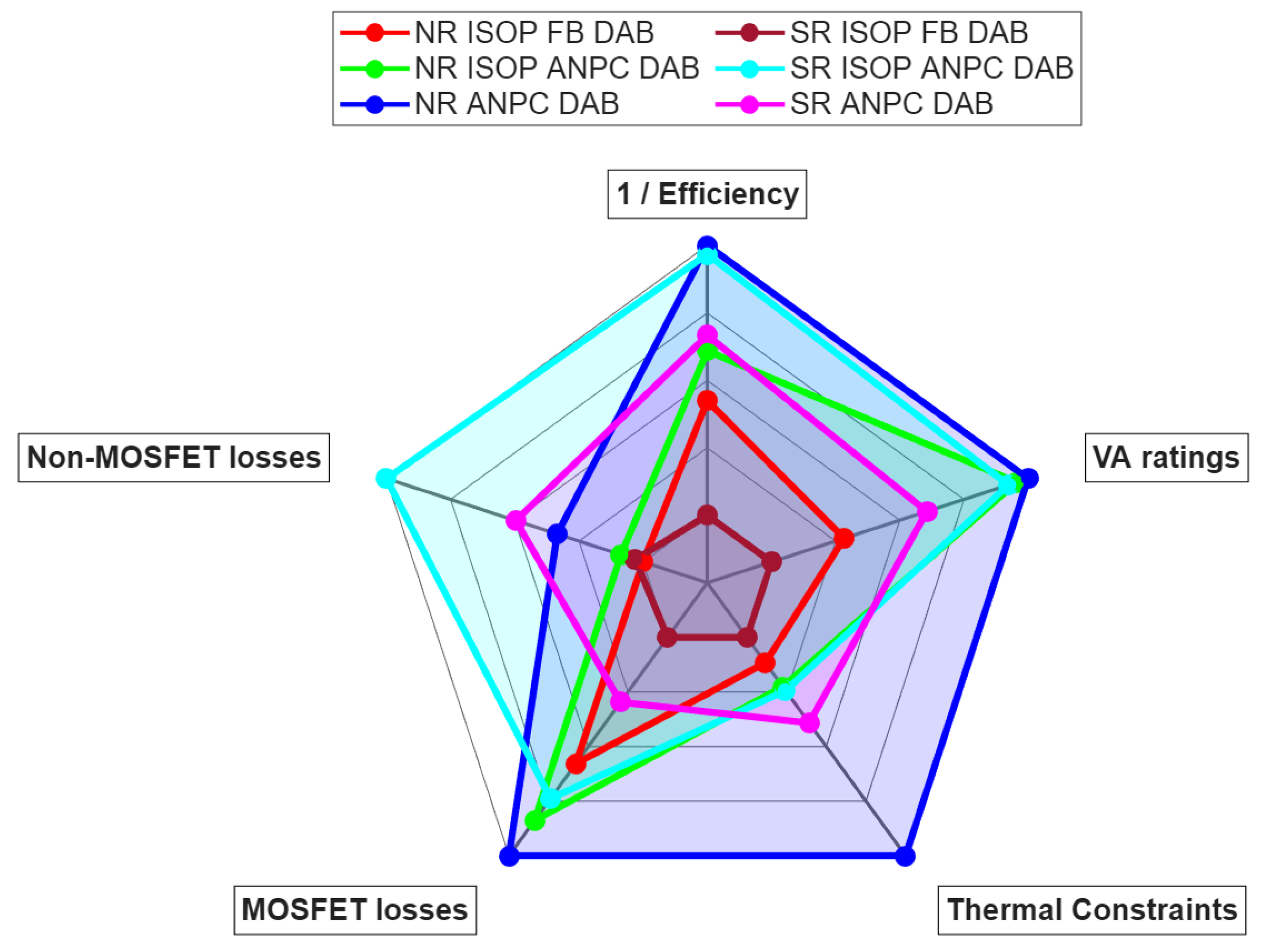
Figure 10 illustrates an overall comparison of the six IBDC topologies based on the results presented in
Section 4 and
Section 5 of this article. The comparison criteria include the normalized values of 1/experimental efficiencies, volt-ampere semiconductor ratings (presented in
Section 5.4), MOSFET losses computed in PLECS using
Table 4 parameters, non-MOSFET losses from
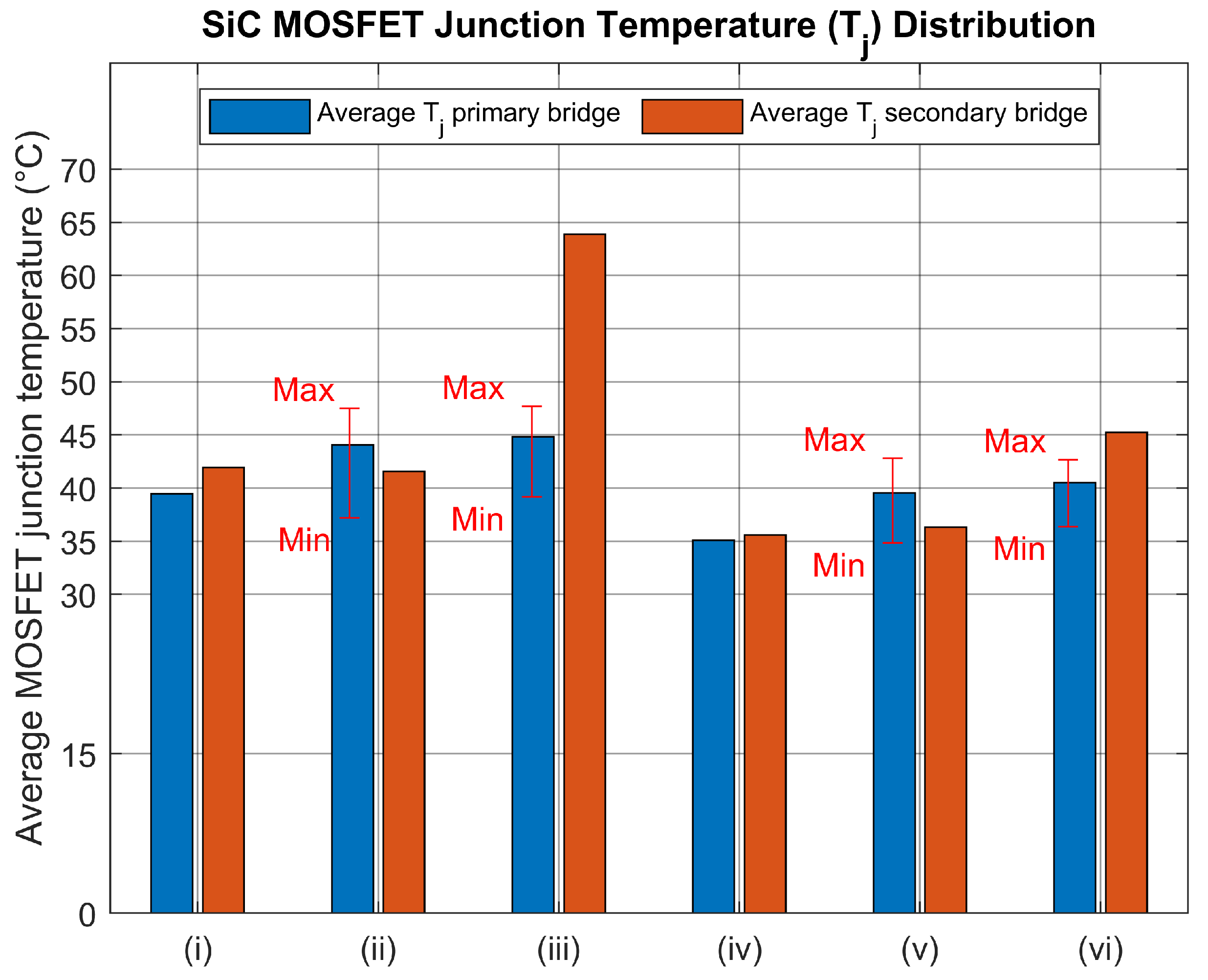
Table 5, and the difference between average junction temperatures of SiC MOSFETs on the primary and secondary active bridges (mentioned as thermal constraints in
Figure 10).
The thermal constraint considered above facilitates comparison of the converters based on the feasibility of a modular heatsink design, as explained in
Section 4.3.
In reference to
Figure 10, the best-performing IBDC topology should have lowest value of 1/efficiency, lowest MOSFET and non-MOSFET losses, lowest VA ratings of SiC MOSFETs, and lowest thermal constraints, i.e., lowest difference between average junction temperatures of SiC MOSFETs on the primary and secondary active bridges. In short, the best-performing topology is represented as the polygon with the smallest area on the spider chart shown in
Figure 10.
In this respect, the SR ISOP FB DAB configuration outperforms the other IBDCs in terms of all the evaluated performance indicators. In addition, it shows promising bidirectional performance for a range of power and EV battery voltage values, as discussed in
Section 6.
Considering the above point and the modular nature of this topology, it can be scaled in terms of power to design a high-power charger of say 350 kW capacity. In such a case, each converter module can be chosen to operate at a power level that achieves maximum efficiency for a wide range of EV battery voltages. For example, at 5 kW power, the efficiency of the SR ISOP FB DAB module is above 96% for the entire EV battery voltage range of 325–425 V in both directions of power flow (see
Figure 9a,b).
The NR ANPC DAB topology has the highest peak current (see
Figure 7c), RMS current (see
Table 5), and turn-off switching losses (see
Figure 4iii) in the secondary active bridge compared to the other configurations. This makes it the least preferred topology in terms of SiC MOSFETs’ VA ratings and efficiency and thermal constraints, as seen from
Figure 10.
From the initial impression, considering the estimated efficiencies calculated using
Table 2 and
Table 5 (blue asterisks in
Figure 8), the series-resonant topologies were expected to have higher efficiencies compared to their non-resonant counterparts. However, considering the experimental efficiencies (red asterisks in
Figure 8), the SR ISOP ANPC DAB and SR ANPC DABs have lower efficiencies than some of the non-resonant topologies. This shows the significance of considering (i) the actual experimental parameters (from
Table 4), (ii) the AC winding resistance and other resistances in the circuit, and (iii) experimentally computed MOSFET losses for the comparison of the IBDC configurations, as discussed in
Section 5.5.
It should also be noted that factors like voltage transformation ratio, series inductance and transformer designs, and the modulation scheme employed significantly influence the efficiency of the topologies for the considered operating conditions. To ensure a fair basis for the performance evaluation presented in this article, all topologies have been evaluated using the same modulation scheme (i.e., single-phase-shift modulation) and voltage transformation ratio.
8. Conclusions
In this article, six 10 kW rated IBDC configurations were compared and analyzed to find the most suitable topology for a modularized and reconfigurable off-board EV charging system with a bipolar DC link. The selection criteria and the design considerations for the considered IBDC configurations were presented. The selected topologies were analyzed based on the VA ratings, loss distribution, and thermal performance of SiC MOSFETs using theoretical analysis and electro-thermal simulations. In addition, the evaluated converters were compared based on the transformer’s voltage and current waveforms, losses from passive components, SiC MOSFETs’ VA ratings considering individual IBDC ratings, and efficiencies obtained from the experiments.
The NR ANPC DAB topology was the least preferred topology considering the majority of the evaluation criteria. The SR ISOP FB DAB topology clearly outperforms the other evaluated IBDCs in terms of efficiency, losses from MOSFETs and passive components, SiC MOSFETs’ VA ratings required, and thermal performance. In addition, its bidirectional operation performance, considering a range of EV battery voltages and powers, is favorable for the construction of a high-power modular fast charger. Therefore, the SR ISOP FB DAB is found to be the best-suited converter configuration for the considered application.
