Article

High-Efficiency Soft-Switching Technique for a Cascaded Buck–Boost Converter Based on Model Predictive Control Using GaN Devices

1
Department of Electrical Engineering, Hanyang University, Seoul 04763, Republic of Korea
2
WP Co., Ltd., Suncheon-si 58023, Republic of Korea
3
Department of Electrical Engineering, Wonkwang University, Iksan-si 54538, Republic of Korea
*
Author to whom correspondence should be addressed.
Electronics 2025, 14(22), 4499; https://doi.org/10.3390/electronics14224499
Submission received: 23 October 2025 / Revised: 11 November 2025 / Accepted: 17 November 2025 / Published: 18 November 2025
(This article belongs to the Section Electronic Materials, Devices and Applications)

Abstract

Improving the efficiency of buck–boost converters has long been a major focus in power electronics. To enhance efficiency and overcome existing limitations, this paper proposes a soft-switching technique for a cascaded buck–boost converter (CBBC). The proposed approach integrates high-frequency switching of four gallium nitride (GaN) devices, improving both dynamic and steady-state performance from hardware and control perspectives. First, a soft-switching modulation scheme based on negative-current pulse width modulation (PWM) is implemented by introducing a new switching sequence in the CBBC, controlled by a modulation variable. This scheme ensures that the GaN switches operate under zero-current switching (ZCS) and zero-voltage switching (ZVS) conditions during transitions. Furthermore, the CBBC operating modes are divided into four intervals for modeling and analysis, upon which a model predictive control (MPC) strategy is developed to achieve fast closed-loop regulation of both output voltage and current. To further minimize current ripple and device losses, the MPC cost function is optimized by constraining the control parameters. Experimental results obtained from a 300-W hardware prototype verify the effectiveness and feasibility of the proposed soft-switching control method.

1. Introduction

With the increasing global demand for electrical energy and the depletion of fossil fuel reserves, coupled with a growing awareness of environmental protection, renewable energy technologies have become a major research focus in recent years [1,2]. Among these technologies, power converters—particularly inverters—play an indispensable role in grid-connected, photovoltaic (PV), and energy storage systems, and have become an essential component of many renewable energy applications [3]. Due to voltage mismatches in such systems, step-up/down power conversion is often required, which is typically realized using buck–boost converter topologies. These converters enable the design of highly regulated DC output voltages from variable input sources [4].
Traditional non-isolated step-up/step-down converters exist in various topologies [5,6,7,8], such as the buck–boost converter, single-ended primary inductor converter (SEPIC), Cuk converter, Zeta converter, Luo converter, and their derivative structures. However, these converters typically employ only one or two active switches and operate with two distinct inductor states—charging and discharging—to achieve step-up or step-down functionality. Moreover, converters operating in continuous conduction mode (CCM) generally exhibit a right-half-plane (RHP) zero, which deteriorates system stability and complicates controller design.
To address the issue of low conversion efficiency, the cascaded buck–boost converter (CBBC) was proposed [9]. This topology employs four switches operating in complementary pairs, enabling multiple charging and discharging states. However, in practical applications, the CBBC suffers from excessively high root-mean-square (RMS) and peak inductor currents, which significantly limit the system’s reliability, efficiency, and overall performance [10,11]. Consequently, several studies have been conducted to mitigate these issues. From a hardware perspective, improvements have been made by replacing the intrinsic body diodes of the internal switches with silicon carbide (SiC) diodes to reduce conduction losses [12]. With the advancement of power semiconductor technology, gallium nitride (GaN) MOSFETs have attracted increasing attention due to their capability for ultra-high switching frequency operation [13,14]. In this work, GaN devices are adopted as the power switches. From a control perspective, various optimization strategies such as soft-switching techniques have been investigated. However, the switching losses of GaN FETs depend not only on the intrinsic characteristics of the GaN chips but also on the parasitic inductances introduced by device packaging and printed circuit board (PCB) layout [15]. These parasitic elements deteriorate the switching transition behavior and further increase switching losses. Therefore, after comprehensive consideration of system performance and implementation constraints, a switching frequency of 100 kHz is selected for the experimental validation. Nevertheless, the high voltage slew rate (dV/dt) of GaN devices tends to increase electromagnetic interference (EMI) emissions [16]. Therefore, it is desirable to design converters that operate with zero-current switching (ZCS) and zero-voltage switching (ZVS) to minimize switching losses and EMI.
To address the control challenges associated with the CBBC converter, a boundary conduction mode (BCM) control strategy has been proposed [17]. In this method, variable-frequency control and optimal timing constraints are introduced to reduce both the RMS and peak values of the inductor current, thereby improving the system’s transient response. This control strategy does not require complex computations or multidimensional lookup tables; instead, it effectively regulates the inductor current by combining soft-switching operation with variable-frequency control, preventing the current from entering the freewheeling stage. Consequently, the CBBC converter efficiency is significantly enhanced [18]. References [19,20] proposed a soft-switching modulation scheme applicable to the CBBC. In this method, a specially designed gating strategy forces the inductor current to take a negative value at the beginning and end of each switching cycle, thereby enabling MOSFET turn-on through the conduction of the anti-parallel body diode. By solving the inductor current equations, the switching intervals of the CBBC are determined, upon which an open-loop control scheme is developed.
Based on the above considerations, this paper proposes a soft-switching control strategy for a cascaded buck–boost converter (CBBC) using model predictive control (MPC). In the proposed approach, the MPC predicts the required duty ratio for the next control interval based on the converter model, enabling rapid voltage regulation and superior dynamic response. Furthermore, by integrating zero-current switching (ZCS) and zero-voltage switching (ZVS) techniques, the proposed system achieves high-efficiency operation.The main contributions of this paper are summarized as follows:
  • A segmented control strategy is proposed, which can be effectively combined with soft-switching operation, providing a theoretical foundation for MPC implementation.
  • A model-based duty-ratio generation scheme is developed, allowing faster voltage reference tracking and improved current transient response compared with conventional PI control.
  • The high-speed switching capability of GaN FETs is fully utilized in conjunction with the MPC strategy to further enhance the converter performance.
The remainder of this paper is organized as follows. Section 2 presents the system modeling and the operating principle of the soft-switching mechanism. Section 3 describes the formulation of the MPC model. Section 4 provides the experimental validation, including the PCB implementation and performance comparison to verify the effectiveness of the proposed approach. Finally, Section 5 concludes the paper.

2. Circuit Configuration and Operating Mechanism

To achieve efficient control of the GaN-based CBBC circuit, this paper establishes a control law that clarifies the relationships among the key parameters, thereby enabling improved regulation performance.

2.1. Topology and Its Segmented Model

As indicated in previous work [21,22], the circuit topology is shown in Figure 1. Owing to its symmetrical structure, the converter enables bidirectional power flow with identical operating characteristics in both directions. In this study, the power flow from left to right is investigated. The CBBC converter consists of four GaN MOSFETs, denoted as S 1 S 4 . To mitigate parasitic oscillations, a damping network composed of the resistance R s n u and the capacitance C o s s is incorporated. C o s s includes not only the capacitance of the RC snubber but also the equivalent capacitance observed from drain to source when the gate and source are shorted. The input voltage, output voltage, and inductor current are defined as v i n , v o u t , and i L , respectively.
Since the system consists of two half-bridge circuits, S 1 and S 2 , as well as S 3 and S 4 , operate in a complementary manner. To establish a control law for the output voltage v o u t and the load current across R, the duty ratios D 1 D 4 are defined according to the different operating states of the GaN FETs.
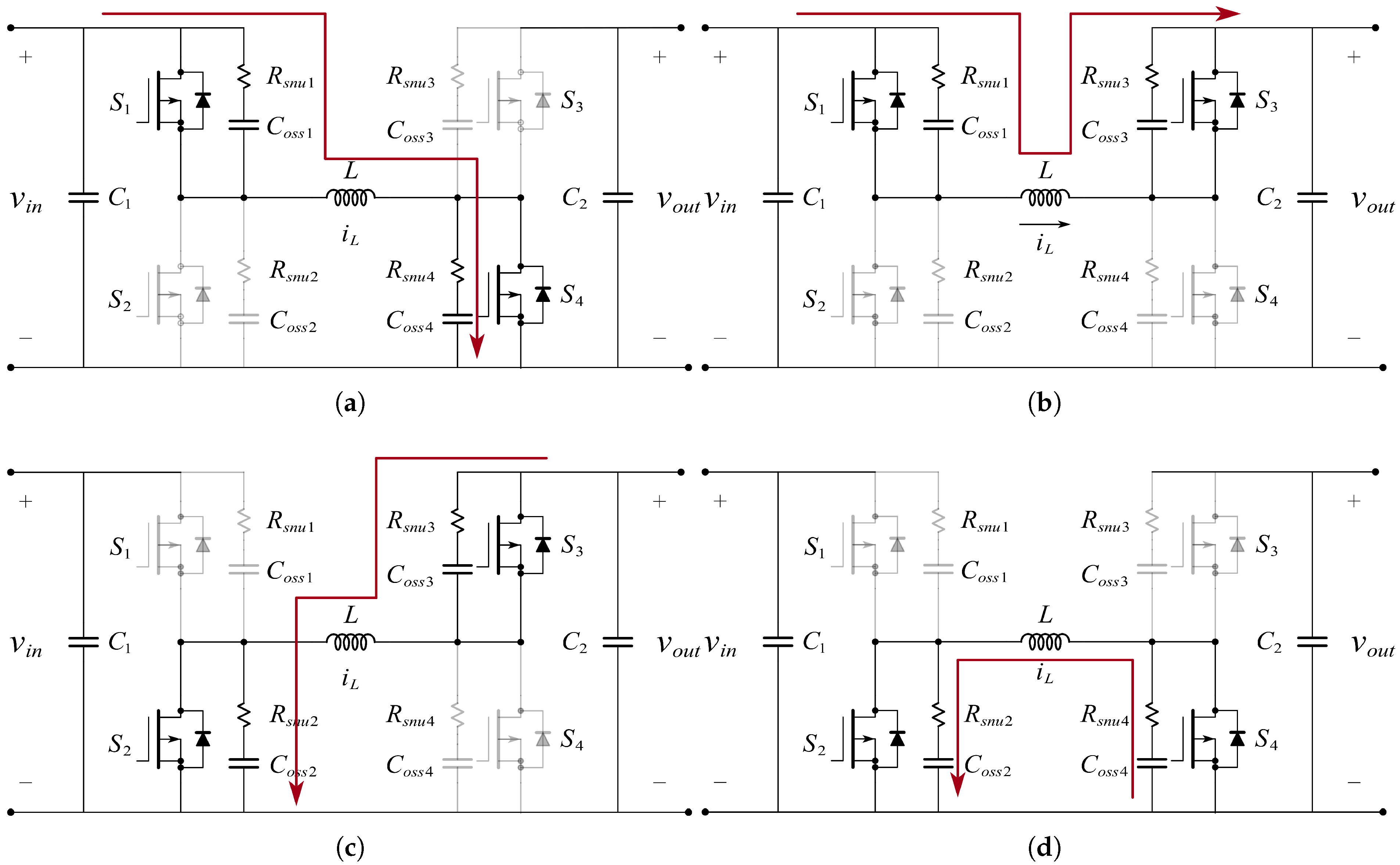
The duty ratios of different operating phases are defined as follows: during the charging phase D 1 , S 1 and S 4 are turned on; during the circulating transition phase D 2 , S 1 and S 3 are turned on; during the discharging phase D 3 , S 2 and S 3 are turned on; and during the freewheeling phase D 4 , S 2 and S 4 conducts. Furthermore, the system state vector is defined as x = [ i L , v o ] T , system input is defined as u = v i n . Based on these definitions, the state-space equations of the converter can be derived as follows:
D 1 : i ˙ L = v i n L , v ˙ o u t = v o u t R C 2 D 2 : i ˙ L = v i n v o u t L , v ˙ o u t = i L C 2 v o u t R C 2 D 3 : i ˙ L = v o u t L , v ˙ o u t = i L C 2 v o u t R C 2 D 4 : i ˙ L = 0 , v ˙ o u t = v o u t R C 2
At this point, the current waveform of the system over a complete cycle can be obtained, as illustrated in Figure 2.

2.2. Discontinuous Conduction Mode

Since GaN devices operate at extremely high switching frequencies, the presence of current during switching transitions can lead to additional switching losses and device stress. Therefore, in the proposed converter, the discontinuous conduction mode (DCM) is adopted as a control strategy to achieve ZVS and to reduce switching stress on the devices. According to the complete control cycle described in the previous section, the average circuit equation over one switching period can be expressed as follows:
i ˙ L = 1 L D 1 v i n D 3 v o u t v ˙ o u t = 1 C 2 D 3 i L v o u t R
According to the duty ratio relationship given in Equation (1), under the DCM condition we have:
v i n v o u t = D 3 D 1 = k
where v i n and v o u t denote the input and output voltages at the current operating point. By combining the system input u and the state vector x defined earlier. Considering that the circuit has two controlled variables, namely the output voltage and the output current, we obtain
x ˙ = f x + g x u f x = k L v o u t 1 R C 2 v o u t , g x = v i n L k i L C 2
By substituting Equations (2) and (3) into Equation (1), the relationship between D 1 and D 3 can be obtained as follows:
D 1 = v o u t D 3 2 + v i n D 1 2 D 3 v o u t v i n
where D 1 denotes the equivalent duty ratio generated by the controller, whereas D 1 represents the actual duty ratio applied to the gate timing after soft-switching mapping. According to the inductor volt–second balance, we have:
D 2 = v o u t D 3 v i n D 1 v i n v o u t

2.3. Principle of Soft Switching

However, when the CBBC operates in DCM, the continuously increasing negative current ( i 0 ) may lead to current backflow. To prevent such reverse conduction, this paper proposes a i 0 -type PWM scheme based on the conventional PWM strategy. The proposed method establishes a continuous current loop when the inductor current becomes negative. Through this mechanism, the inductor current is maintained at i 0 until the end of the present switching period, enabling the design of a dedicated soft-switching sequence based on i 0 .
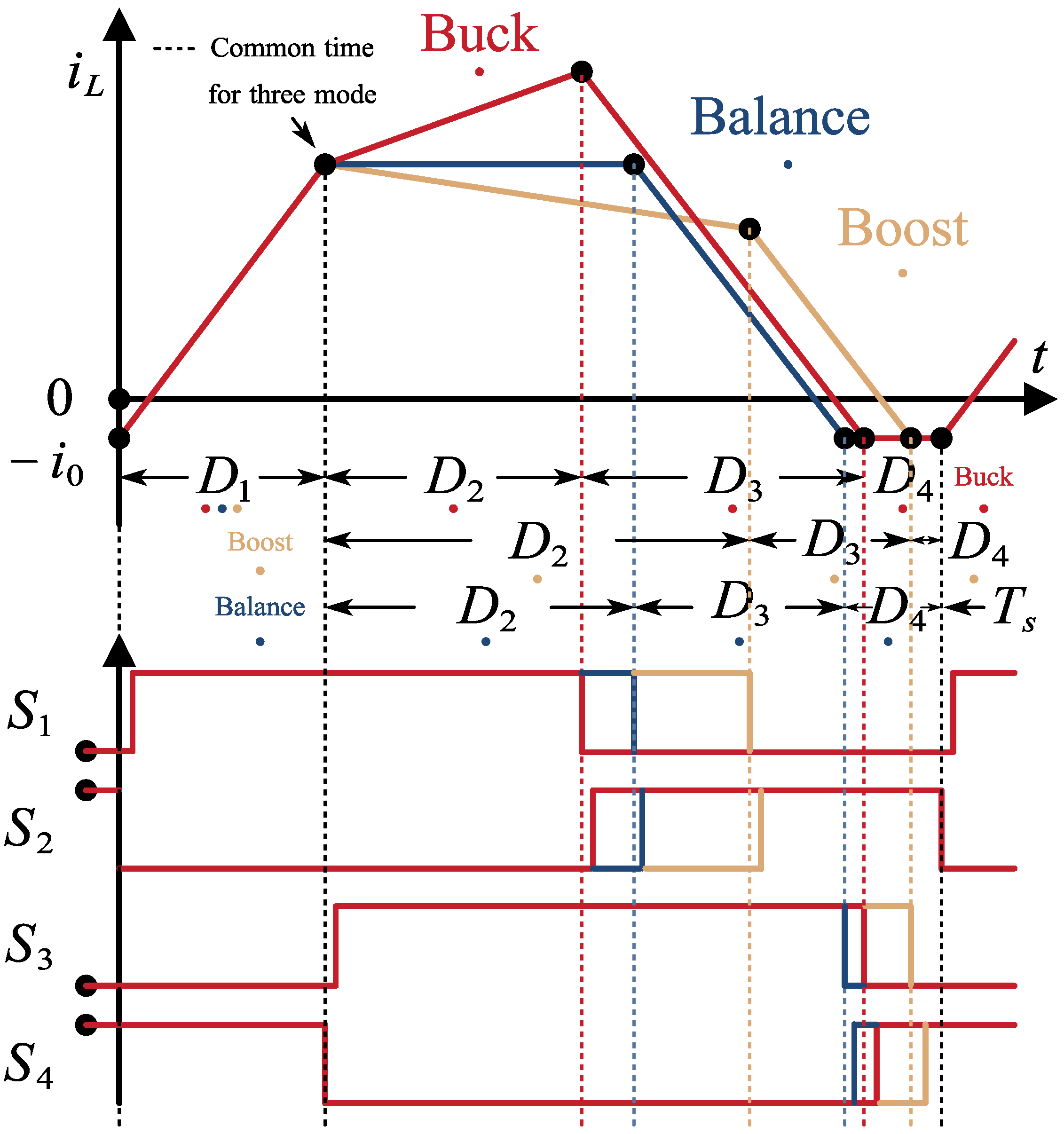
Based on the soft-switching principle and the four control methods discussed in the previous section, the relationship between the CBBC operating modes and the duty ratios is obtained, as illustrated in Figure 3. To illustrate more clearly the relationship among the buck, boost, and balanced operating states, it is assumed that D 1 remains constant, while the variations in D 2 , D 3 , and D 4 are used to analyze their effects on the system output.
From Figure 3, it can be observed that the output operating mode is determined by the relative magnitudes of D 3 and D 1 , which reflect the influence of the duty ratio variation on the two sets of GaN FETs. In addition, conventional dead time is included in the control signals of each switch. From the relationships among i 1 , i 2 , and the duty ratios illustrated in Figure 3, the steady-state expression can be derived as follows:
i 1 = v i n L D 1 T s i 0 i 2 i 1 = v i n v o u t L D 2 T s i 2 = v o u t L D 3 T s i 0 1 = D 1 + D 2 + D 3 + D 4
To clarify the functional relationship among the steady-state duty ratios D 1 , D 2 , D 3 , and D 4 , and to establish a direct connection between Equations (5)–(7) is simplified as follows:
D 3 = i 2 + i 0 / T s v o u t L
Based on DCM, further loss reduction at high switching frequencies requires selecting either zero-current switching (ZCS) or zero-voltage switching (ZVS), and ensuring that the GaN FETs operate under the chosen condition during turn-on and turn-off transitions. The criteria for distinguishing between the two switching methods can be described as follows:
ZVS : 0 t d e a d i L t d t Q o s s , H + Q o s s , L = Q o s s , ZCS : i G A N t o f f = 0
Here, Q denotes the equivalent electric charge observed from drain to source when the gate and source are shorted, whereas i G A N refers to the intrinsic current of the switching device. In addition, t o f f represents the instant at which the GaN FET is turned off. In the ZVS calculation, the dead time t d e a d is considered. As the inductor current during D 4 in Equation (1) can be approximated as constant, combining this with Equation (6) yields the condition that the dead time must satisfy in order to achieve ZVS:
Q o s s , i n e g t d e a d L R ln i n e g i m i n
Set the zero current be denoted as i 0 . The average current through capacitor C 2 can then be expressed in terms of the duty ratios as follows:
C 2 d v o u t d t = v i n 2 2 L v o u t D 1 2 T s v o u t R
At this point, the relationship between the duty ratio D 1 and the output voltage can be obtained. The perturbation signals are defined as v ( t ) = v o u t ( t ) V o u t 0 and d ( t ) = D 1 ( t ) D 1 , 0 . Then applying a first-order Taylor expansion to Equation (8) and then taking its Laplace transform, we obtain:
s C 2 v s = 2 R v s + v i n 2 T s L D 1 v o u t d s
G s = v s d s = v i n 2 D 1 R T s L C 2 R v o u t s + 2 L v o u t
Accordingly, the stability criterion of the system can be obtained, as illustrated in Figure 4.
As shown in Figure 4, the controlled plant maintains a relatively stable gain at low frequencies. However, when the variation frequency of the control input, duty ratio reaches 100 kHz, a phase delay of approximately 90 is introduced into the system. This also indicates that the output voltage is limited at high frequencies by the dynamics of the LC filter and the converter components, thereby posing additional challenges to the control performance.

3. Formulation of Model Predictive Control

The system model has been derived in the previous chapter. This chapter focuses on formulating a control law that enables simultaneous regulation of the output voltage and current. Conventional control methods, such as PI control, rely heavily on parameter tuning to regulate current and voltage. Since there is no direct physical coupling between these two quantities, the control performance largely depends on empirical adjustments, which often leads to unsatisfactory results. Therefore, this paper adopts a model predictive control (MPC) approach to achieve predictive regulation of both current and voltage.

3.1. Model Construction for MPC

Linearizing the Equation (4) at the operating point ( x 0 , u 0 ) yields:
δ x ˙ = A δ x + B δ u , y = C δ x A = f x + g x u x 0 , u 0 , B = g x x 0 , u 0
where matrices A = 0 0 0 1 / ( R C 2 ) , B = v i n / L v o u t / L 0 i L / C 2 and C = i L are obtained from Equation (4). After discretizing Equation (14), we obtain:
δ x k + 1 = A d δ x k + B d δ u k , A d = e A T s , B d = 0 T s e A τ d τ B
To eliminate the steady-state error, an integrator is introduced to perform error tracking of v o u t .
z k + 1 = z k + r k C x k , y k = C x k , C = [ 0 1 ]
By incorporating the required integrator into the augmented state, we obtain:
x ¯ = δ x k z v , k z i , k , A ¯ = A d 0 0 e v T 1 0 e i T 0 1 , B ¯ = B d 0 0 , C ¯ = C 0 0
To adapt the controller for microcontroller-based implementation, the prediction horizon k and the control period T s are introduced. Based on the discretized model, the predictive model of the MPC can be expressed in a multi-step matrix form as follows:
x k + 1 = A ¯ x k + B ¯ Δ u k , y k = C ¯ x k
where Δ u k = u k u k 1 , which represents the incremental form of the prediction. At this stage, the model construction of the MPC is completed. Based on the developed model, the state-space equation for the MPC has been established. On this basis, it is necessary to consider the relationship between the desired optimization objectives and the controlled plant.

3.2. Formulation of the Cost Function

After constructing the model used for the MPC, the next step is to formulate the cost function. Based on the two controlled variables, we establish the following expression:
J = i = 1 N w i i o u t i o u t * 2 + w v v o u t v o u t * 2 + Δ D 2
i o u t * and v o u t * indicate the reference value. w i and w v represent the weighting factors associated with the output current and output voltage, respectively, reflecting the relative importance of each controlled variable. The term Δ D denotes the variation in the duty ratio, which is constrained to limit excessive fluctuations in the system output.
Meanwhile, for other physical quantities, applying soft constraints to the outputs after defining the objective function is also essential.
i L i m a x , 0 v o u t v m a x
D 3 D 3 , m i n , D 1 0 , D 1 + D 3 1
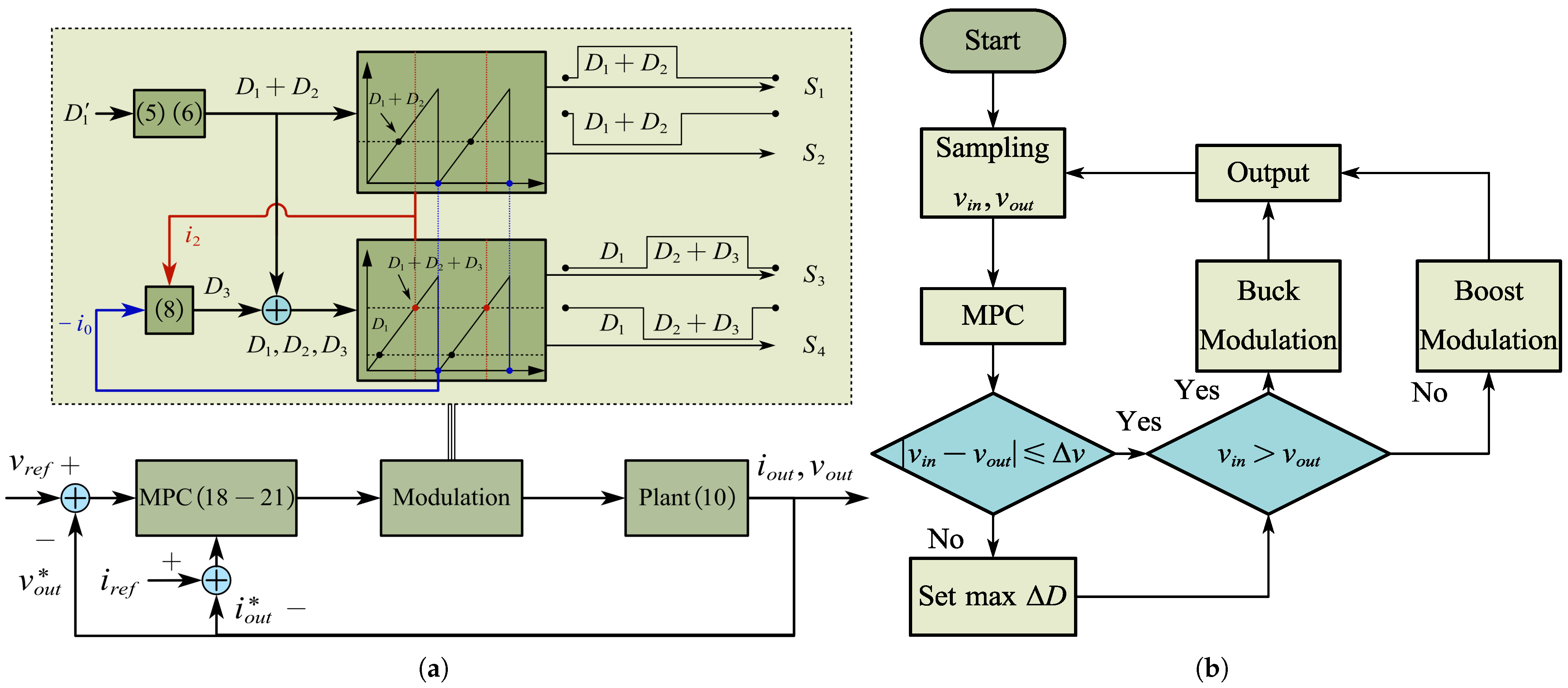
At this stage, the control block diagram and flowchart of the proposed MPC-based soft-switching control scheme for the cascaded buck–boost converter are obtained, as shown in Figure 5. It can be observed that the system adopts a dual closed-loop structure for voltage and current regulation. Moreover, since the GaN devices are configured as two half-bridge pairs, phase synchronization is maintained within each switching cycle. This synchronization facilitates the development of an accurate and compact model, enabling the implementation of a simplified control algorithm. It should also be noted that the performance of the MPC depends on the model parameters, which are influenced by factors such as temperature and switching frequency. These effects represent a promising direction for future research and are not discussed in detail in this paper.
Unlike conventional soft-switching converters that require additional resonant or auxiliary circuits to achieve ZVS/ZCS [23,24], the proposed control method realizes soft-switching through MPC. The controller predicts the inductor current and switch-node voltage at each sampling instant, and adaptively determines the optimal switching sequence that satisfies ZVS conditions without the aid of extra resonant components. As a result, the converter maintains soft-switching operation over a wide load range while simplifying the circuit structure.

4. Experiment

The proposed CBBC hardware prototype has been implemented with a rated power of 300 W. The converter features a wide input voltage range covering 24–60 V, as shown in Figure 6. The design parameters of the CBBC are determined based on the operating conditions corresponding to the widest input voltage range, as summarized in Table 1.
Since the PCB is a prototype designed primarily for experimental validation, its physical area was not considered a design constraint. This, to some extent, affects the thermal dissipation capability. In addition, to eliminate the influence of leakage current on controller performance, a single-point grounding scheme was implemented between the DSP control section and the power stage.
Regarding the snubber circuit parameters in the PCB, according to the description in [25], the capacitor C o s s must be charged to the target voltage within the minimum turn-off time. The lower limit of the capacitance is then determined based on the desired voltage overshoot. A suitable value is selected within this range, and a capacitance of 4.7 pF is adopted in the prototype PCB. In addition, according to the charge balance requirement and the power dissipation considerations derived from the formula in [25], the corresponding resistance R s n u is chosen to be 50 Ω .
In this experiment, the classic DSP TMS320F28335 from Texas Instruments (Dallas, TX, USA) is employed as the main control unit. It operates at a clock frequency of 150 MHz and provides 68 kB of on-chip RAM, which is sufficient to execute the MPC algorithm at a sampling frequency of 100 kHz. The inductor current as well as the input and output currents are measured using the ACS37002 current sensor from Allegro MicroSystems (Manchester, NH, USA), which converts the measured current into a voltage signal within a range of ±4.5 V. The PI parameters were tuned using the conventional design method to achieve stable and fast response. As a result, the voltage loop gains were set to k p v = 0.15 and k i v = 9.8 , while the current loop gains were set to k p i = 2.3 and k i i = 4.8 .

4.1. Dynamic and Steady-State Response Results

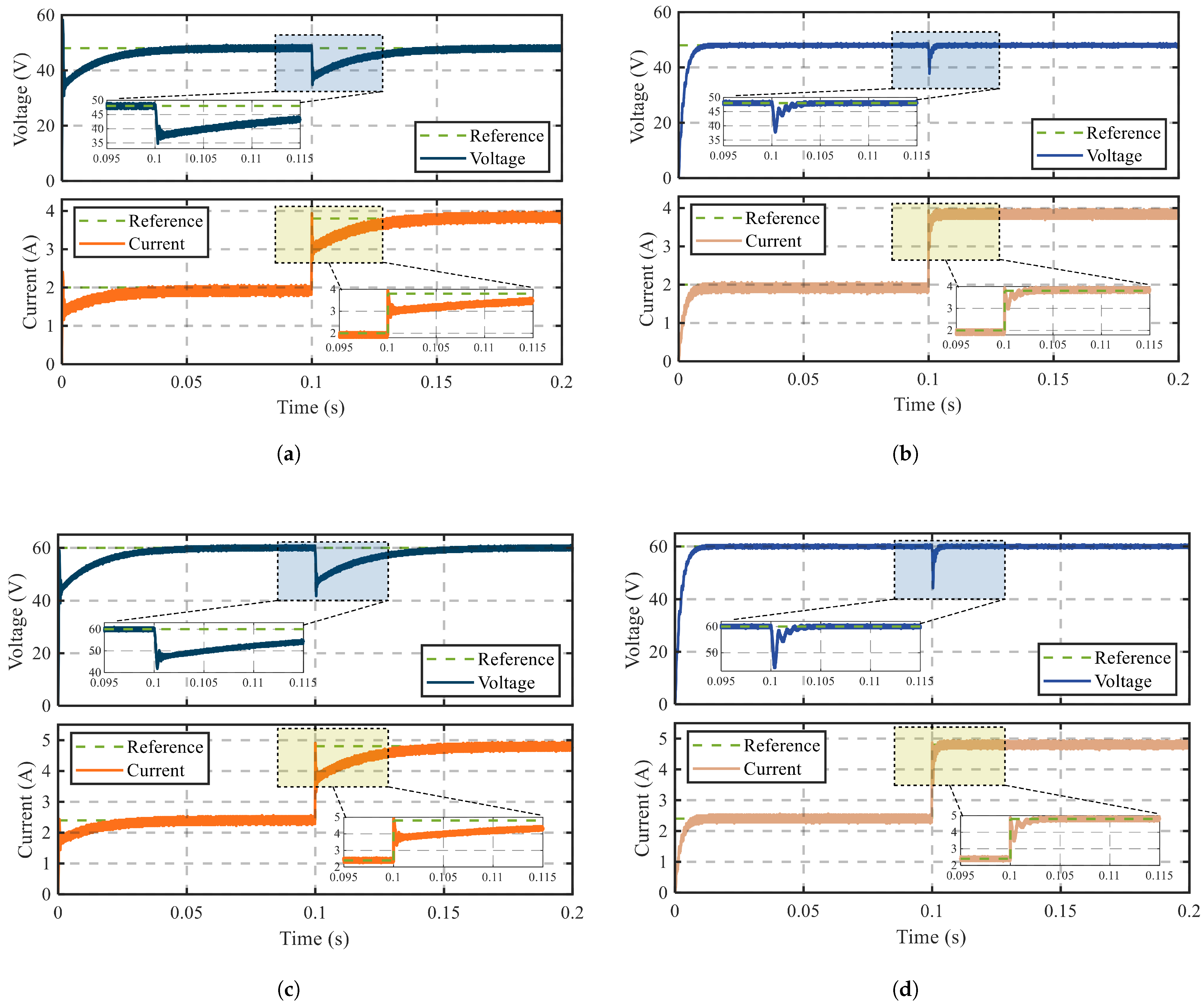
Figure 7 presents the dynamic response experiments under a load variation from 25 Ω to 12.5 Ω at 0.1 s. The performance of both the PI-controlled system and the MPC-controlled system is compared. In Figure 7a,b, the input voltage is 60 V with an output reference of 48 V, whereas in Figure 7c,d, the input voltage is 48 V and the output reference is 60 V.
By defining the settling time as the duration required for the output to reach 93% of the reference value, it can be observed that, in the buck mode, the conventional PI controller requires 36.2 ms to regulate the output voltage and current, whereas the MPC achieves the same response within 14.4 ms, resulting in a 60.2% improvement in dynamic response time. Similarly, the minimum output voltage obtained with the PI controller is 34.8 V, while that of the MPC is 38.6 V. In the boost mode, the PI controller takes 38.5 ms to complete the transient response, whereas the MPC only requires 11.3 ms, yielding a 70.7% reduction in response time. In terms of current control, the MPC also demonstrates a clear advantage. Under PI control, the current overshoot reaches 4.95 A and requires 39.1 ms to settle, whereas the MPC exhibits a smaller overshoot of 4.82 A with a settling time of only 7.9 ms. Therefore, it can be concluded that the MPC provides overall superior control performance compared with the conventional PI controller.
To verify the effectiveness of the proposed negative-current i 0 soft-switching technique and evaluate its impact on efficiency improvement, the inductor current i L was selected as the observation variable, since it is difficult to directly measure the voltage and current across the GaN devices.
Figure 8 and Figure 9 show the inductor current i L waveforms for the PI-based and MPC-based control algorithms, respectively, under three operating modes: buck mode ( V i n = 60 V, V i n = 48 V), boost mode ( V i n = 48 V, V i n = 60 V), and steady-state mode ( V i n = 48 V, V i n = 48 V). Because the current flowing through the GaN device is difficult to measure directly, the current of the power pole is used as an equivalent measurement. It can be observed that when the control signal of S1 is converted to 24 V through the gate driver, the voltage across the GaN device drops to nearly zero. The current flows through the reverse conduction path of the GaN FET channel and the snubber network, thereby achieving soft-switching operation.
The measured waveforms confirm that the proposed control successfully achieves ZVS in both Buck and Boost modes without any auxiliary resonant circuits, validating that the soft-switching effect is obtained purely by the predictive control strategy.
It can also be observed that the absolute value of the negative current i 0 in the MPC algorithm is 0.1 A smaller than that in the PI-controlled system. According to Equation (9) and [26], this indicates that the capacitor utilization in the MPC-controlled converter is higher than that of the conventional PI algorithm, as shown in the following equation:
i 0 m a x v i n , v o u t C o s s L
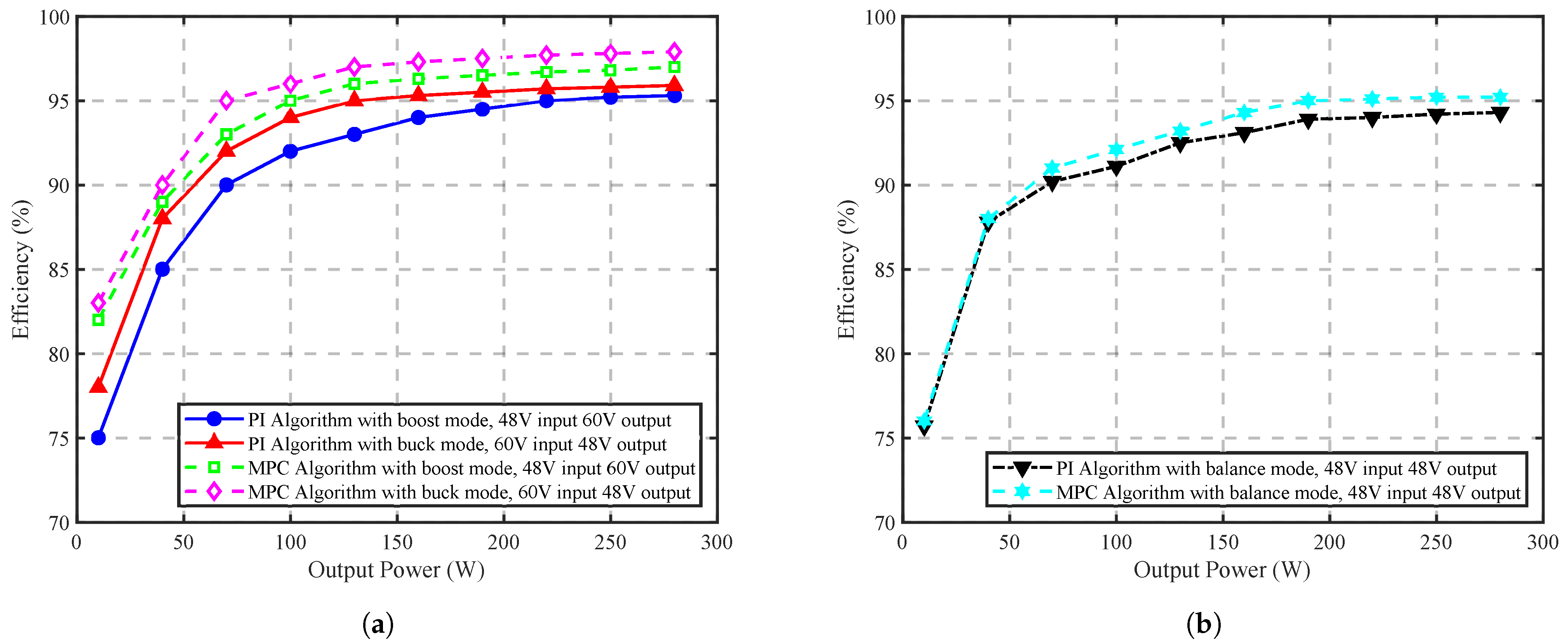
Figure 10 presents four efficiency curves, illustrating the performance of both the PI and MPC algorithms under buck, boost and balance operating modes. These curves are used to compare and analyze the impact of different control algorithms and operating modes on the overall system efficiency.
It can be observed that, in terms of overall efficiency, the boost mode exhibits 0.6–1% lower efficiency than the buck mode when operating near the rated power. In addition, the MPC algorithm achieves approximately 2% higher efficiency compared with the PI control. This improvement can be attributed not only to the smaller steady-state deviation between the output voltage, current and their reference values in MPC, but also to the fact that the PI parameters may not be perfectly tuned. Since the MPC performs prediction based on an accurate model, it achieves smaller steady-state error and consequently higher conversion efficiency.
It is noteworthy that, under the balanced operating mode, the absolute value of the negative inductor current i L in the MPC-controlled system is smaller than that in the conventional case. This indicates that a smaller current magnitude is sufficient to achieve the soft-switching condition, further demonstrating that the coordination between MPC and the soft-switching technique is superior to that of the PI control.
Table 2 summarizes the peak efficiencies of the two control algorithms under different operating modes and rated conditions. A comparison of the maximum efficiencies reveals that the control accuracy of each algorithm can affect the overall performance by approximately 0.5–1%. In addition, at low power levels, the efficiency drops sharply due to increased inductor losses under low-current conditions [27]. Overall, the proposed soft-switching control scheme maintains high efficiency across a wide operating range.

4.2. Discussion

Although GaN devices are capable of operating at high switching frequencies, a switching frequency of 100 kHz was selected in this study to balance switching loss, electromagnetic interference (EMI), and control accuracy. Operating at excessively high frequencies in a prototype converter would increase parasitic effects, gate-driver losses, and measurement noise, making it difficult to clearly verify the proposed soft-switching operation and control performance.
The measured efficiency of the prototype is relatively low compared with the theoretical expectation for GaN-based converters. This is mainly attributed to non-ideal factors in the experimental setup, such as magnetic core losses, gate-driver power consumption, and PCB parasitic inductances. Meanwhile, the prototype exhibits a certain sensitivity to temperature variations.
The primary objective of the prototype experiment is to verify the feasibility of the proposed soft-switching strategy based on MPC. In future work, the efficiency will be further improved and the scalability of the proposed method will be validated by optimizing the magnetic component design and high-frequency PCB layout, aiming to increase the operating frequency beyond 300 kHz, and the investigation of temperature sensitivity will also be a key focus of future work.

5. Conclusions

This study proposes a control framework for a cascaded buck–boost converter based on model predictive control. Compared with the conventional PI dual-loop control, the proposed MPC scheme provides a more accurate determination of the duty ratio by utilizing model parameters. By integrating discontinuous conduction mode operation and soft-switching techniques, the proposed method achieves improved dynamic and steady-state performance, leading to higher overall efficiency. Furthermore, the operating principle of the cascaded buck–boost converter is presented, and its control cycle is modeled to theoretically ensure the feasibility of the proposed control algorithm. Finally, the experimental results validate the superior performance and effectiveness of the proposed MPC-based strategy.

Author Contributions

Conceptualization, L.L. and J.D.; methodology, L.L.; software, J.D.; validation, J.L. and S.K.; formal analysis, C.J.; investigation, J.L.; resources, S.K. and C.J.; data curation, L.L. and J.D.; writing—original draft preparation, L.L.; writing—review and editing, J.D. and J.L.; visualization, S.K.; supervision, J.L. and C.J.; project administration, J.L.; funding acquisition, C.J. All authors have read and agreed to the published version of the manuscript.

Funding

This research was supported by the Ministry of SMEs and Startups (MSS), Republic of Korea, under project number S3401318.

Data Availability Statement

The original contributions presented in the study are included in the article; further inquiries can be directed to the corresponding author.

Conflicts of Interest

Seonheui Kang was employed by the company WP Co., Ltd. The remaining authors declare that the research was conducted in the absence of any commercial or financial relationships that could be construed as a potential conflict of interest.

References

  1. Bull, S.R. Renewable energy today and tomorrow. Proc. IEEE 2001, 89, 1216–1226. [Google Scholar] [CrossRef]
  2. Dincer, I. Renewable energy and sustainable development: A crucial review. Renew. Sustain. Energy Rev. 2000, 4, 157–175. [Google Scholar] [CrossRef]
  3. Umuhoza, J.; Zhang, Y.; Zhao, S.; Mantooth, H.A. An adaptive control strategy for power balance and the intermittency mitigation in battery-PV energy system at residential DC microgrid level. In Proceedings of the 2017 IEEE Applied Power Electronics Conference and Exposition (APEC), Tampa, FL, USA, 26–30 March 2017; pp. 1341–1345. [Google Scholar]
  4. Kim, D.; Lee, B.; Hur, J. Light-load efficiency improving algorithm in cascaded buck-boost converter. In Proceedings of the 2015 18th International Conference on Electrical Machines and Systems (ICEMS), Pattaya, Thailand, 25–28 October 2015; pp. 448–451. [Google Scholar]
  5. Chen, Z. PI and sliding mode control of a Cuk converter. IEEE Trans. Power Electron. 2012, 27, 3695–3703. [Google Scholar] [CrossRef]
  6. Hwu, K.I.; Peng, T.J. A novel buck–boost converter combining KY and buck converters. IEEE Trans. Power Electron. 2011, 27, 2236–2241. [Google Scholar] [CrossRef]
  7. Banaei, M.R.; Bonab, H.A.F. A high efficiency nonisolated buck–boost converter based on ZETA converter. IEEE Trans. Ind. Electron. 2019, 67, 1991–1998. [Google Scholar] [CrossRef]
  8. Gholizadeh, H.; Sharifi, S.R.; Hashemi, M.R.; Afjei, E.; Saman, A.G. Design and implementation a single-switch step-up DC-DC converter based on cascaded boost and luo converters. Energies 2021, 14, 3584. [Google Scholar] [CrossRef]
  9. Chen, X.; Pise, A.A.; Batarseh, I. Magnetics-based efficiency optimization for low power cascaded-buck-boost converter. IEEE Trans. Circuits Syst. I Regul. Pap. 2020, 67, 5611–5623. [Google Scholar] [CrossRef]
  10. Cheng, Z.; Li, Z.; Li, S.; Gao, J.; Si, J.; Das, H.S.; Dong, W. A novel cascaded control to improve stability and inertia of parallel buck-boost converters in DC microgrid. Int. J. Electr. Power Energy Syst. 2020, 119, 105950. [Google Scholar] [CrossRef]
  11. Tian, L.; Liu, H.; Zhang, Y.; Wu, X. A Reduced-Order Small-Signal Model for Four-Switch Buck–Boost Under Soft-Switching Current Shaping Control Strategy. Electronics 2025, 14, 2564. [Google Scholar] [CrossRef]
  12. Waffler, S.; Kolar, J.W. A novel low-loss modulation strategy for high-power bidirectional buck + boost converters. IEEE Trans. Power Electron. 2009, 24, 1589–1599. [Google Scholar] [CrossRef]
  13. Jones, E.A.; Wang, F.F.; Costinett, D. Review of commercial GaN power devices and GaN-based converter design challenges. IEEE J. Emerg. Sel. Top. Power Electron. 2016, 4, 707–719. [Google Scholar] [CrossRef]
  14. Yang, X.; Zhang, R.; Yang, Q.; Song, Q.; Litchford, E.; Walker, A.J.; Pidaparthi, S.; Drowley, C.; Dong, D.; Li, Q.; et al. Evaluation and MHz Converter Application of 1.2-kV Vertical GaN JFET. IEEE Trans. Power Electron. 2024, 39, 15720–15731. [Google Scholar] [CrossRef]
  15. Huang, X.; Liu, Z.; Li, Q.; Lee, F.C. Evaluation and Application of 600 V GaN HEMT in Cascode Structure. IEEE Trans. Power Electron. 2013, 29, 2453–2461. [Google Scholar] [CrossRef]
  16. Bang, T.; Park, J.W. Development of a ZVT-PWM buck cascaded buck–boost PFC converter of 2 kW with the widest range of input voltage. IEEE Trans. Ind. Electron. 2017, 65, 2090–2099. [Google Scholar] [CrossRef]
  17. Yu, J.; Liu, M.; Song, D.; Su, M. A soft-switching control for cascaded buck-boost converters without zero-crossing detection. IEEE Access 2019, 7, 32522–32536. [Google Scholar] [CrossRef]
  18. Chen, X.; Pise, A.A.; Elmes, J.; Batarseh, I. Ultra-highly efficient low-power bidirectional cascaded buck-boost converter for portable PV-battery-devices applications. IEEE Trans. Ind. Appl. 2019, 55, 3989–4000. [Google Scholar] [CrossRef]
  19. Lee, I.O.; Moon, G.W. Half-bridge integrated ZVS full-bridge converter with reduced conduction loss for electric vehicle battery chargers. IEEE Trans. Ind. Electron. 2013, 61, 3978–3988. [Google Scholar] [CrossRef]
  20. Roschatt, P.M.; Pickering, S.; McMahon, R.A. Bootstrap voltage and dead time behavior in GaN DC–DC buck converter with a negative gate voltage. IEEE Trans. Power Electron. 2015, 31, 7161–7170. [Google Scholar] [CrossRef]
  21. Callegaro, L.; Ciobotaru, M.; Fletcher, J.E.; Rios, P.A.; Pagano, D.J. Design of cascaded control loop for solar power optimizer based on a buck-boost converter. In Proceedings of the 2016 IEEE 2nd Annual Southern Power Electronics Conference (SPEC), Auckland, New Zealand, 5–8 December 2016; pp. 1–6. [Google Scholar]
  22. Guler, N.; Komurcugil, H.; Bayhan, S.; Abu-Rub, H. Simplified single-stage buck-boost rectifier with proportional-integral and cascaded proportional-resonant control method. IEEE Trans. Ind. Electron. 2023, 71, 348–359. [Google Scholar] [CrossRef]
  23. Dey, S.; Mallik, A. An Online-Optimized ZVS-Current Tracked Soft-Switching Modulation for Triple Active Bridge Converter. IEEE Trans. Power Electron. 2024, 39, 14708–14728. [Google Scholar] [CrossRef]
  24. Tian, G.; Chen, S.; Ding, X.; Peng, J.; Kou, Z. Isolated High Step-up Soft-switching quasi-Zsource DC-DC Converter. IEEE Access 2024, 12, 49927–49936. [Google Scholar] [CrossRef]
  25. Kim, J.; Park, S.; Lee, J.; Cho, J.; Cho, G.; Kim, H. A Floating Voltage Source-Based Turn-Off Snubber for a Nonisolated Multilevel SiC DC-DC Converter. IEEE Trans. Ind. Electron. 2025, 72, 390–400. [Google Scholar] [CrossRef]
  26. Alajmi, B.N.; Marei, M.I.; Abdelsalam, I.; Ahmed, N.A. Multiphase Interleaved Converter Based on Cascaded Non-Inverting Buck-Boost Converter. IEEE Access 2022, 10, 42497–42506. [Google Scholar] [CrossRef]
  27. Wu, C.C.; Liu, C.Y.; Wang, G.B.; Shieh, Y.T.; Chieng, W.H.; Chang, E.Y. A new GaN-based device, P-cascode GaN HEMT, and its synchronous buck converter circuit realization. Energies 2021, 14, 3477. [Google Scholar] [CrossRef]
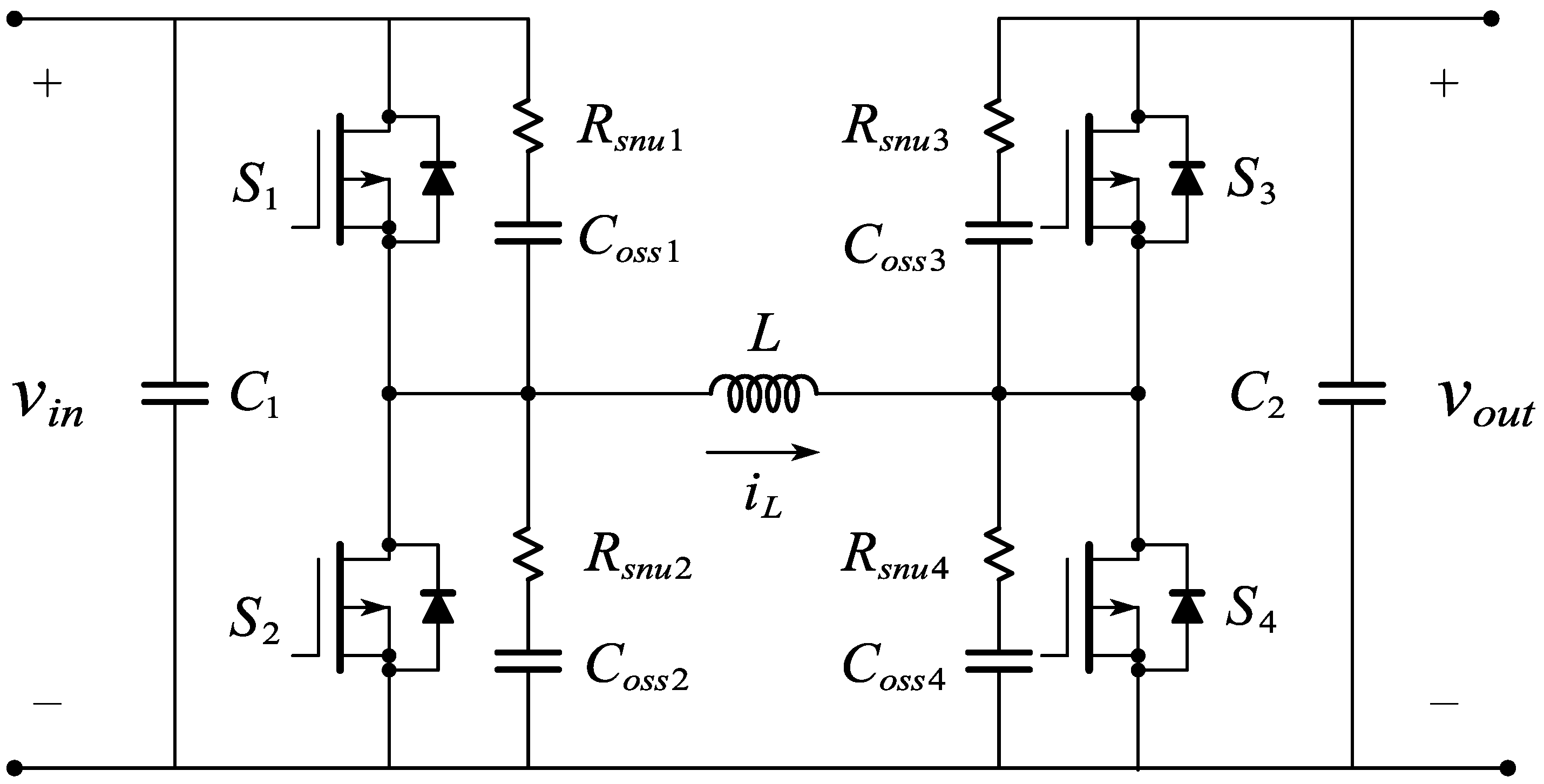
Figure 1. Electrical circuit diagram of the CBBC.
Electronics 14 04499 g001
Figure 2. Current flow (in red) diagrams of the CBBC in four operating states: (a) Current path during D 1 when S 1 and S 4 are ON. (b) Current path during D 2 when S 1 and S 3 are ON. (c) Current path during D 3 when S 2 and S 3 are ON. (d) Current path during D 4 when S 2 and S 4 are ON.
Electronics 14 04499 g002
Figure 3. Inductor current waveforms of the negative-current i 0 -based PWM under buck, boost, and balanced operating modes with D 1 assumed as a constant value.
Electronics 14 04499 g003
Figure 4. Bode plot of the transfer function for the equivalent system.
Electronics 14 04499 g004
Figure 5. Framework and flowchart of the proposed control strategy: (a) Block diagram of the control strategy and controlled plant. (b) Flowchart of the proposed MPC algorithm.
Electronics 14 04499 g005
Figure 6. Overview of the experimental test platform: (a) Prototype PCB of the GaN-based cascaded buck–boost converter. (b) Test setup of the PCB prototype.
Electronics 14 04499 g006
Figure 7. Comparison of voltage and current responses between the conventional PI control and the proposed MPC control under boost and buck modes: (a) Dynamic voltage and current response of PI control during step-up from 48 V to 60 V. (b) Dynamic voltage and current response of MPC strategy during step-up from 48 V to 60 V. (c) Dynamic voltage and current response of PI control during step-down from 60 V to 48 V. (d) Dynamic voltage and current response of MPC strategy during step-down from 60 V to 48 V.
Electronics 14 04499 g007
Figure 8. Inductor current i L waveforms of the conventional PI control under buck, boost, and balanced modes: (a) i L waveform of PI control during step-down from 60 V to 48 V. (b) i L waveform of PI control during step-up from 48 V to 60 V. (c) i L waveform of PI control under balanced operation at 48 V to 48 V.
Electronics 14 04499 g008
Figure 9. Inductor current i L waveforms of the proposed MPC control under buck, boost, and balanced modes: (a) i L waveform of MPC control during step-down from 60 V to 48 V. (b) i L waveform of MPC control during step-up from 48 V to 60 V. (c) i L waveform of MPC control under balanced operation at 48 V to 48 V.
Electronics 14 04499 g009
Figure 10. Power and efficiency distributions of the PI and MPC strategies under buck, boost and balance operating modes: (a) Buck and boost mode comparison. (b) Balance mode comparison.
Electronics 14 04499 g010
Table 1. Specifications of the Proposed GaN-Based Buck Boost Converter.
ParametersDescriptionValues
P n o u t Rated Output Power300 W
V i n Input Voltage20–60 V
V o u t Output Voltage20–60 V
T s Switching frequency100 kHz
S 1 , 2 , 3 , 4 Boost/Buck switch (GS61008T)GaN, 100 V/90 A @25 °C
LInductor (7443643300)0.33 mH, 250 V/30 A @20° C
C 1 Input Capacitor190 μ F, 100 V @25 °C
C 2 Output Capacitor470 μ F, 100 V @25 °C
R s n u Snubber Resistance50 Ω , 150 V/0.5 W @20 °C
C o s s Snubber Capacitor4.7 pF, 100 V @25 °C
Table 2. Peak value of efficiency of modulations.
Operation ModeBuck ModeBoost ModeBalance Mode
PI Method95.9%95.3%94.3%
MPC Method97.9%96.9%95.2%
Disclaimer/Publisher’s Note: The statements, opinions and data contained in all publications are solely those of the individual author(s) and contributor(s) and not of MDPI and/or the editor(s). MDPI and/or the editor(s) disclaim responsibility for any injury to people or property resulting from any ideas, methods, instructions or products referred to in the content.