Article

A Class-F High-Power Rectifier Circuit Based on Admittance Matching

1
College of Mechanical and Electrical Engineering, University of Electronic Science and Technology of China, Chengdu 611731, China
2
Tianfu Jiangxi Laboratory, Chengdu 641419, China
*
Authors to whom correspondence should be addressed.
Electronics 2025, 14(22), 4461; https://doi.org/10.3390/electronics14224461 (registering DOI)
Submission received: 12 September 2025 / Revised: 15 October 2025 / Accepted: 12 November 2025 / Published: 16 November 2025

Abstract

This paper proposes a novel high-efficiency microwave rectifier circuit with a three-stage harmonic control network based on admittance matching technology. The microwave rectifier circuit is mainly composed of a three-stage Class-F harmonic control network, an admittance matching structure, and a DC filtering structure. The three-stage Class-F harmonic control network, featuring a simple structure, not only achieves the control of the second and third harmonics but also performs impedance control on the fourth harmonic to further improve efficiency, while also realizing the impedance matching function. The DC filtering structure eliminates traditional LC components to reduce losses; meanwhile, it uses fan-shaped microstrip lines to achieve filtering and completes admittance matching with the three-stage harmonic control network. This paper presents the simulation, fabrication and measurement of a high-power rectifier circuit. The results of the measurement show that at 2.55 GHz, with an input power of 32.5 dBm, the rectifier circuit achieves a maximum rectification efficiency of 76.9%, exhibiting excellent high-power performance. Additionally, it addresses the difficulty of impedance-matching technology being relatively complex for parallel circuits. The use of admittance for matching provides valuable reference significance for reducing the complexity of parallel circuit matching and enhancing the intuitiveness of matching in related research.

1. Introduction

In recent years, with the continuous development of new energy technologies, there has been an increasing demand for cable-free charging and high-power charging. As one of the research directions in wireless power transfer [1,2,3,4,5], Wireless Microwave Power Transfer (WMPT) [6,7,8,9] technology enables wireless charging by transmitting microwave energy, featuring advantages such as cable-free operation, long transmission distance [10], and high levels of flexibility. WMPT systems have a wide range of applications, extending to drone charging stations, wireless phone charging, mobile smart devices and new energy vehicles. They have also emerged as a research theme of interest to an increasing number of scholars [11,12,13].
As one of the key circuits in WMPT systems, the function of the microwave rectifier circuit is to convert the microwave energy captured by antennas into direct current (DC) energy, which is then used to power subsequent device charging. The performance of the microwave rectifier circuit determines the transmission performance of the entire WMPT system [14,15]; therefore, research on microwave rectifier circuits is of great importance. The performance indicators of rectifier circuits are mainly reflected in aspects such as high power [16], wide power range [17,18], micro power, wide frequency band, wide load range, and small size and so on. However, as society develops, there is a growing demand for high-power charging, particularly for smartphones and new energy vehicles. A high-power charging system can significantly reduce charging times, enhancing convenience in people’s lives. Consequently, it is crucial to investigate the high-power performance metrics of rectifier circuits [19,20,21,22].
The rectifier circuit’s power capacity is primarily determined by the reverse breakdown voltage of its core component, which is the diode. A higher reverse breakdown voltage of the diode allows the rectifier circuit to withstand higher input power. If the voltage across the diode exceeds its reverse breakdown voltage, the diode will be damaged by breakdown, and the rectifier circuit will cease to function. To increase the reverse breakdown voltage of diodes, gallium nitride (GaN) Schottky diodes manufactured using third-generation semiconductor technology can be adopted, as they exhibit a high reverse breakdown voltage (BV > 50 V). In Article [23], a GaN Schottky diode was used to design a high-power microwave rectifier circuit. Owing to advanced manufacturing processes, this diode achieved an extremely high reverse breakdown voltage of 164 V, and this diode is characterized by minimal junction capacitance (0.32 pF) and reduced series resistance (4.5 Ω). When employed in a 5.8 GHz high-power microwave rectifier, the circuit attained a peak rectification efficiency of 71% under an input power of 34 dBm, with a maximum input power capacity of 38 dBm, demonstrating excellent performance. However, this series of diodes has not been widely commercialized, so silicon-based Schottky diodes with lower reverse breakdown voltages (BV < 50 V) have to be used instead. To realize high-power rectifier circuits using silicon-based Schottky diodes, methods such as multi-diode series-parallel connection or the addition of power dividers can be employed to increase the input power capacity. In Article [21], a silicon-based Schottky diode (model: HSMMS-282P) was used to draw up the design for a high-power microwave rectifier circuit. A single HSMS-282P package integrates 4 diodes connected in series-parallel, significantly improving the diode’s power capacity within the same package area. The HSMS-282P Schottky diode serves as the foundation for a designed high-power rectifier featuring a voltage doubler architecture: at an operating frequency of 433 MHz, its rectification efficiency exceeded 66% within an input power range of 22–33 dBm, with a maximum input power of 33 dBm and a peak rectification efficiency of 79%. A similar design scheme was also presented in Article [24], where 4 HSMS-282P diodes were connected in series-parallel—this configuration allowed the diodes and the die to be connected in a series-parallel way, which made it possible to increase the input power capacity a lot. At 2.45 GHz, the measured maximum input power reached 33 dBm, with a rectification efficiency of 66.8%. While the series-parallel configurations in Articles [19,25] and the use of power divider structures lead to a substantial improvement in the power capacity of rectifier circuits, the rectification efficiency remains relatively low due to increased losses caused by the diodes and power divider structures.
However, the rectifier circuits mentioned above still suffer from insufficient efficiency, large size, and poor stability. To overcome these shortcomings, this paper proposes a novel Class-F high-power microwave rectifier circuit based on admittance matching. First, a silicon-based Schottky diode (model: HSMS-270B) with a relatively high reverse breakdown voltage (BV = 25 V) was selected. Second, an extremely simple three-stage Class-F harmonic control network was adopted, consisting of an open-circuited λ/8 microstrip line, a short-circuited λ/12 microstrip line, and an open-circuited λ/16 microstrip line. Not only does this network facilitate harmonic control, it also enables impedance matching. An additional stage in the harmonic control network also contributes to higher rectification efficiency. Finally, a fan-shaped microstrip line was used at the output end: it not only fulfills the filtering function but also completes admittance matching with the three-stage harmonic control network. This design eliminates the high-frequency losses associated with traditional LC low-pass filters, addresses the current difficulty of impedance matching for parallel circuits, enhances the rectifier circuit’s ability to resist load changes, and improves circuit stability. The design and simulation of the Class-F high-power rectifier were carried out by using ADS (2022) software, followed by prototype fabrication and testing. Measurement results show that at 2.55 GHz, the circuit can achieve a high input power of 32.5 dBm (1.78 W), a rectification efficiency of 76.9%, a DC output power of 1.37 W, and a DC output voltage of 11.2 V.

2. Design of the Class-F High-Power Rectifier

The structure of a novel three-stage Class-F high-power microwave rectifier circuit based on admittance matching is illustrated in Figure 1. This rectifier circuit is mainly composed of three parts: a three-stage Class-F harmonic control network, an admittance matching structure, and a DC filtering structure. Among them, the three-stage Class-F harmonic control network consists of λ/8, λ/12, and λ/16 microstrip lines. The admittance matching structure is composed of two sections of admittance matching microstrip lines: an impedance matching stub (Match_Turn) and a DC filtering + impedance matching component (Filter&Match). This admittance matching structure can reduce the matching complexity of the rectifier circuit and enhance the intuitiveness of matching. Specifically, the Filter&Match admittance matching microstrip line (length: 9.94 mm/width: 1.89 mm) is connected in parallel behind the λ/4 fan-shaped microstrip line; the Match_Turn admittance matching microstrip line (length: 9.94 mm/width: 1.89 mm) is connected in series behind the three-stage Class-F harmonic network; finally, the other ends of the two admittance matching microstrip lines are connected in parallel. The DC filtering structure is composed of a λ/4 fan-shaped microstrip line (FML_λ/4) and an admittance matching microstrip line (Filter&Match). This DC filtering structure functions to filter out radio frequency (RF) signals while allowing DC signals to pass through. The dimensions of the λ/4 fan-shaped microstrip line are 11.8 mm in radius and 70° in angle. The Filter&Match admittance matching microstrip line (length: 9.74 mm/width: 1.89 mm) is connected in parallel behind the λ/4 fan-shaped microstrip line, and the other end of the fan-shaped microstrip line is connected to the load resistor (RL) at the output end of the rectifier circuit.

2.1. Design of Third Harmonic Control Network

The three-stage Class-F harmonic control network consists of one section of λ/8 microstrip line, one section of λ/12 microstrip line, and one section of λ/16 microstrip line. Due to the nonlinear characteristics of the rectifier diode, harmonic voltages and harmonic currents are generated. This harmonic control network can not only reduce the diode’s loss through waveform reshaping but also reflect the 2nd, 3rd, and 4th harmonics back to the diode for re-rectification, thereby improving rectification efficiency. According to Class-F harmonic impedance control theory, the voltage across the diode presents a square wave in the time domain when all even-order harmonics exhibit short-circuit low impedance and all odd-order harmonics exhibit open-circuit high impedance., while the current presents a half-sine wave. These two waveforms are completely offset by 90 degrees, resulting in a zero overlap area between the voltage and current waveforms in the time domain. Under this condition, the loss within the diode amounts to zero, while the ideal rectification efficiency of the Class-F circuit attains 100%. A harmonic control network with more stages can reduce diode loss and further improve rectification efficiency. When additionally processing the 4th harmonic, the efficiency can be further increased. When controlling harmonics beyond the 4th order, the harmonic control network yields little improvement in efficiency. Moreover, an excessive number of harmonic control networks will increase insertion loss, while also raising design complexity and enlarging the size. As a result, with reference to research literature and application scenarios, a three-stage harmonic control network is selected for the design. Considering the balance between the overall dimensions of the rectifier and the insertion loss inherent to the harmonic control network itself, our design selectively controls the second, third, and fourth harmonics. In terms of the specific circuit structure, one end of the diode is connected in series with a λ/12 microstrip line before being grounded; the other end is connected in parallel with two open microstrip lines, whose lengths are λ/8 and λ/16, respectively. To analyze the characteristics of this network, we employed the fundamental input impedance Formula (1) to derive the impedance values exhibited by the λ/8, λ/12, and λ/16 microstrip lines at both the fundamental frequency and the target harmonic frequencies. These derived results are presented in the following Equations (2)–(4). It can be inferred from the formulas that the λ/12 short-circuited microstrip line exhibits high impedance (∞) at the 3rd harmonic; the λ/8 and λ/16 open-circuited microstrip lines exhibit low impedance (0) at the 2nd and 4th harmonics, respectively. This meets the harmonic control theory of Class-F circuits [18]. As shown in Equations (2)–(4), this Class-F harmonic control network successfully reshapes the voltage and current waveforms across the diode, making the voltage approximate a half-sine wave and the current approximate a square wave. Different from traditional Class-F harmonic control networks, which only perform impedance control on the 2nd and 3rd (two-stage) harmonics to reduce diode loss and improve rectification efficiency, the present invention proposes a novel three-stage Class-F harmonic control network. It not only realizes impedance control on the 2nd and 3rd harmonics but also on the 4th harmonic. It has further improved efficiency and performs a pivotal function in enhancing the efficiency of the rectifier circuit.
Z i n p u t = Z 0 Z L + j Z 0 tan ( β l ) Z 0 + j Z L tan ( β l )
Z λ / 8 ( ω ) = j Z 8 cot π 4 ω ω 0 = j Z 8                                                         ω =   ω 0 0                                                                       ω =   2 ω 0  
Z λ / 12 ( ω ) = + j Z 12 tan π 6 ω ω 0 = j Z 12                                               ω =   ω 0                                                     ω =   3 ω 0  
Z λ / 16 ( ω ) = + j Z 16 tan π 8 ω ω 0 = j 6.85 * 10 3 Z 1                 ω =   ω 0 0                                                                   ω =   4 ω 0  

2.2. Design of DC Filter&Match

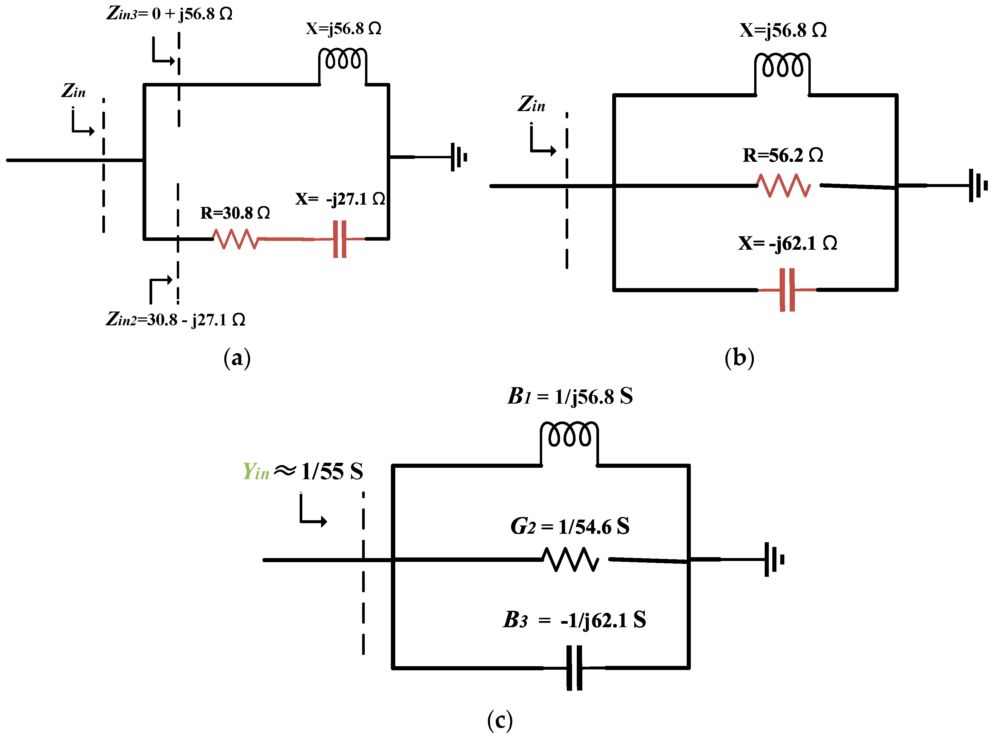
Next, the derivation of the fundamental wave admittance matching process is carried out. The input impedance looking into the third harmonic control terminal can be obtained through simulation in ADS, where Zin1 is given by (5). After connecting in series with the admittance matching microstrip line Match_Turn, the input impedance Zin2 is (6). At this point, the input impedance (6) can be equivalent to an equivalent circuit consisting of a 30.8 Ω resistor in series with a −27.1 Ω capacitor. Meanwhile, the input impedance of another section of the admittance matching microstrip line Filter&Match Zin3 is (7), and this input impedance (7) can be equivalent to an inductor of j56.8 Ω. As shown in Figure 2a, the two sections of the admittance matching lines are in a parallel structure. Since the two input impedances connected in parallel cannot be directly added, the series circuit of (6) is converted into a 54.6 -j62.1 Ω parallel equivalent circuit. This results in an equivalent circuit shown in Figure 2b, which consists of a 54.6 Ω resistor, a -j62.1 Ω capacitor, and a j56.8 Ω inductor, all connected in parallel. The converted parallel equivalent circuit is in the form of impedance, so the above three parallel impedance equivalent circuits are converted into three parallel admittance equivalent circuits. Since these are input impedances, this structure still cannot be directly summed. Therefore, the above three parallel equivalent circuits of impedance are converted into three series equivalent circuits of admittance, so that admittances can be directly summed. The converted admittance equivalent circuit is composed of a G 2 conductance, a B 3 susceptance, and a B 1 susceptance connected in series, as shown in Equation (8). The summed admittance value is Yin = 1/54.6 − j665.5 S, which is approximately equal to Yin = 1/55 S. Converted to impedance, it is approximately Zin = 55 Ω input impedance, which is very close to the ideal matching condition of 50 Ω. Finally, the admittance matching is completed, and this process is shown in Figure 2c. Thus, we have completed the theoretical derivation of the fundamental wave admittance matching for the rectifier circuit. This admittance matching structure can reduce the complexity of the rectifier circuit matching and enhance the intuitiveness of the matching.
Z i n 1 = 108.32 j 22.579
Z i n 2 = 30.815 j 27.128
Z i n 3 = 0 + j 56.8
Z i n   = Z i n 2 Z i n 3 = 1 Y in = 1 B 1 + G 2 + B 3 = 55 Ω
For the through-filtering terminal, this paper adopts a fan-shaped microstrip line to form a low-pass filter, which allows direct current (DC) to pass through while blocking both the fundamental wave and harmonics. A capacitor Cin = 24 pF is connected in series at the radio frequency (RF) input terminal. This capacitor functions as a DC blocking capacitor, preventing direct current components from entering the RF input port. This protects sensitive signal sources from overcurrent damage and avoids DC power dissipation. The capacitor permits radio frequency signals to pass through with minimal insertion loss. The device utilizes a 0402 package (dimensions approximately 1.0 mm × 0.5 mm), making it suitable for high-density printed circuit board designs. Generally, a smaller package results in lower losses at high frequencies. The impact of this capacitor on the rectifier’s input impedance is minimal, and it barely participates in the matching process. The resistive load at the DC output terminal is R L = 120 Ω. The diode used is a Schottky diode model HSMS270B, and its model parameters are based on the official datasheet provided by Anglo. This diode features a high reverse breakdown voltage of 25 V and a low-loss resistance of 0.65Ω, making it highly suitable for high-power rectifier circuits.

3. Measuring and Simulating the Class-F High-Power Rectifier

Combining the third-harmonic control network described in Section 2.1 and Section 2.2 with DC filtering and the admittance structure results in a novel high-efficiency microwave rectifier circuit with a simplified Class F harmonic network. The circuit board material used for this rectifier circuit is Teflon 300CA-C, which has a relative permittivity of 2.94 and a loss tangent of 0.0016; the overall circuit size is 3.99 cm × 3.1 cm. The rectifier circuit was designed and simulated using industrial design software (ADS). This paper presents the simulation, fabrication (via board printing and processing) and experimental testing of the rectifier circuit. Figure 3 shows the layout diagram and actual prototype of the rectifier circuit.
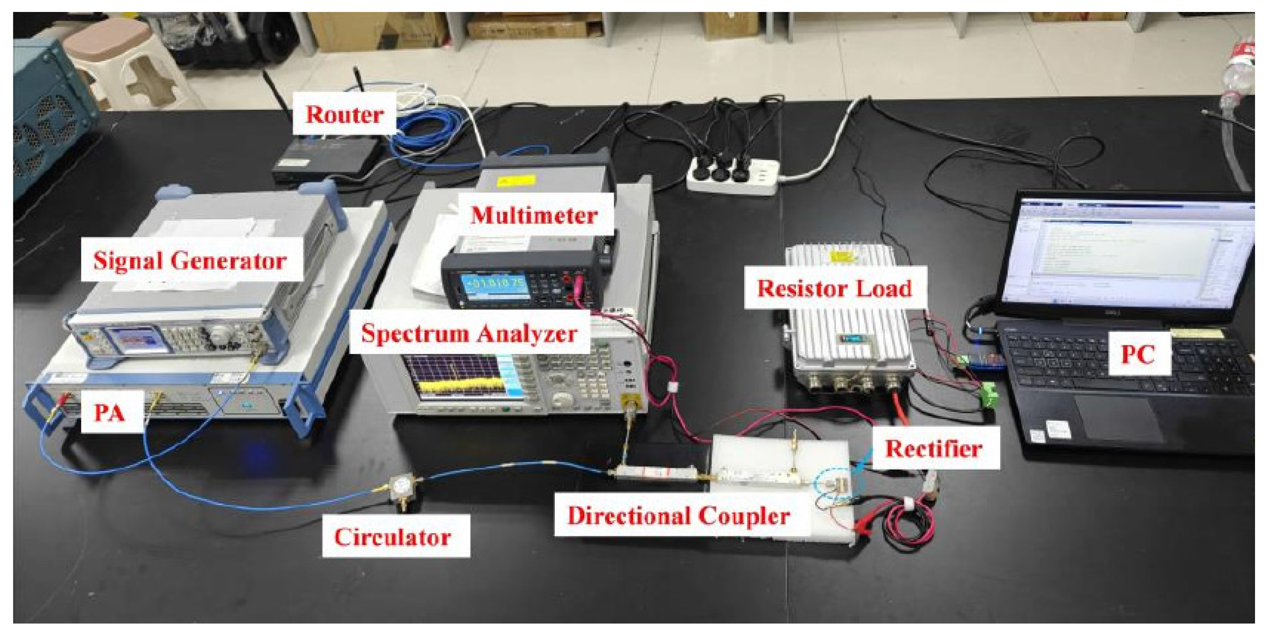
In contrast to the conventional approach of measuring low-power microwave rectifier circuits, the rectifier circuits require connecting an additional power amplifier externally to the signal source to drive them. The rectifier measurement system consists of seven main components: signal generator, broadband power amplifier, spectrum analyzer, desktop multimeter, programmable resistor box, directional coupler, and circulator. The system test framework is illustrated as follows. The signal (ROHDE) is used to establish an RF signal source, which can output up to 23 dBm of RF power to the broadband power amplifier, providing energy for subsequent amplification of the signal by the amplifier. The broadband power amplifier (RFAMP-004060G-20W) is used to amplify the signal from the signal source and transmit it to the rectifier circuit under test, with a maximum output of 43 dBm of RF signal and a working bandwidth of 0.8 GHz to 5 GHz. The spectrum analyzer (KEYSIGHT CXA N9000A) is used to monitor the signal energy at the coupled end of the directional coupler, and then calculates the actual RF power input to the rectifier circuit through the coupling degree of the directional coupler. The desktop multimeter is employed for monitoring the voltage throughout the rectifier circuit’s load resistor, which is used to calculate the DC power output of the rectifier circuit. The programmable resistor box (RW20W-20K-R1) is used as the load resistor of the rectifier, and the resistance value of the resistor box can be varied and can withstand high power. It is also used to calculate the rectifier circuit’s DC power output. The directional coupler (SHWDCP-0506-30SFFF) couples a portion of that energy to the spectrum analyzer for monitoring the rectifier circuit’s input power, with a coupling degree of approximately 30 dB. A 10 dB attenuator is added to the coupled end to avoid damaging the spectrum analyzer. The circulator (UIYBCC3234A) is used to avoid damage to the broadband power amplifier caused by the energy reflected by the rectifier circuit. After compensating for the error values of the entire test device in the circuit, the voltage across the load resistor and the RF input power supplied to the rectifier circuit can be measured. The rectifier circuit’s efficiency can be determined by using Formula (9). In Formula (9), efficiency represents the rectifier efficiency, P D C is the DC output power, Pin is the microwave input power, Vout is the DC voltage across the load resistor, and RL is the load resistor.
Equation (9) represents the efficiency of the rectifier circuit.
P D C denotes the DC output power.
P in signifies the microwave input power.
V o u t represents the DC voltage across the load resistor.
R L is the load resistor.
e f f i c i e n c y = P D C P in × 100 % = V o u t 2 / R L P i n × 100 %
The simulation and actual measurement curves of the Class F high-power microwave rectifier circuit are shown in Figure 4. Harmonic control can be divided into Class-F harmonic control and continuous Class-F harmonic control. Among them, Class F is narrowband harmonic control for a single frequency point. Continuous Class-F, based on Class-F, incorporates a continuous parameter factor α, which enables it to function as a wideband harmonic control. Specifically, Class-F belongs to narrowband harmonic control. Only at a single frequency point can the 90-degree overlap between the square voltage waveform and the half-sinusoidal current waveform be achieved. This minimizes diode loss and thereby brings the highest efficiency. Under the condition that the Class-F harmonic topology designed for 2.55 GHz is fixed, any frequency deviation will make the system deviate from Class-F harmonic control. This further leads to an increase in the overlapping area of voltage and current waveforms, an increase in diode loss, and consequently a decrease in efficiency. Therefore, the rectifier circuit under the Class F harmonic control structure achieves the highest efficiency at 2.55 GHz. (Refer to references on Class-F for details). Continuous Class F does not have the problem of rapid efficiency decline due to slight frequency deviation. The introduction of the continuous parameter factor α allows the voltage and current waveforms within a wide frequency band to approximate a square voltage waveform and a half-sinusoidal current waveform with 90-degree overlap—though they are not strictly square or half-sinusoidal. Thus, continuous Class-F serves as wideband harmonic control. Although continuous Class-F has a wider bandwidth than Class-F, its efficiency is slightly lower because its waveforms are not ideal. If continuous Class-F were adopted in this study, 2.55 GHz might no longer be the frequency point with the highest efficiency. To sum up, due to the inherent narrowband limitation of Class-F harmonic control, the rectifier circuit in this study achieves the highest efficiency at 2.55 GHz.
The effective operating frequency range of the circuit designed in this paper is 2.35–2.65 GHz, within which the rectification efficiency can reach over 70%, and its peak efficiency point is at 2.55 GHz with a stable DC output. There are slight differences between the simulation efficiency and the measured efficiency, but they are basically consistent on the whole (especially in the context of microwave circuit design, this degree of difference is within a reasonable range and does not affect the judgment of the overall consistency between simulation and actual performance). Simulation and measurement Efficiency is shown in Figure 5. When the operating frequency of the rectifier circuit is 2.55 GHz, for the simulation, the input power range of the rectifier circuit is 15~32 dBm. When the input power reaches the maximum value of 32 dBm, the simulated and measured rectification efficiencies reach their maximum values, which are 79.6% and 76.6%, respectively, with a difference of only 3% between the two efficiencies. The load variation range of this rectifier circuit during operation is 50~130 Ω. At 90 Ω, the simulated and measured efficiencies are 79.6% and 76.6%, respectively, reaching the highest efficiency. As illustrated in Table 1, it compares the rectification efficiency performance of the relevant rectifier circuits corresponding to different literatures. The rectifier circuit meets the expected high-power design specifications, and the simulation results are in good agreement with the actual measurement results.

4. Conclusions

A novel Class F high-power rectifier circuit based on admittance matching is proposed in this paper. It adopts a three-stage Class F harmonic control network, and the admittance matching structure and DC filtering structure together form the high-power rectifier circuit. The actual measurement of this high-power microwave rectifier circuit at 2.55 GHz shows that the maximum peak efficiency can reach 76.9% under an RF power input of 32.5 dBm. While this high-power rectifier circuit achieves high efficiency and high-power energy transmission, the novel admittance matching technology significantly reduces the complexity of parallel circuit matching and enhances the intuitiveness of matching. The demand for high-power energy transmission can be met by this Class F high-power microwave rectifier circuit, which is well suited to MWPT systems.

Author Contributions

Conceptualization, X.-N.L., L.-F.T., L.-F.D., T.W., G.-C.Z. and Y.-Q.C.; Methodology, X.-N.L., L.-F.T., L.-F.D., T.W., G.-C.Z. and Y.-Q.C.; Software, X.-N.L., L.-F.T., L.-F.D., T.W., G.-C.Z. and Y.-Q.C.; Validation, X.-N.L., L.-F.T., L.-F.D., T.W., G.-C.Z. and Y.-Q.C.; Formal analysis, X.-N.L., L.-F.T., L.-F.D., T.W., G.-C.Z. and Y.-Q.C.; Investigation, X.-N.L., L.-F.T., L.-F.D., T.W., G.-C.Z. and Y.-Q.C.; Resources, X.-N.L., L.-F.T., L.-F.D., T.W., G.-C.Z. and Y.-Q.C.; Data curation, X.-N.L., L.-F.T., L.-F.D., T.W., G.-C.Z. and Y.-Q.C.; Writing—original draft, X.-N.L., L.-F.T., L.-F.D., T.W., G.-C.Z. and Y.-Q.C.; Writing—review & editing, X.-N.L., L.-F.T., L.-F.D., T.W., G.-C.Z. and Y.-Q.C.; Visualization, X.-N.L., L.-F.T., L.-F.D., T.W., G.-C.Z. and Y.-Q.C.; Supervision, X.-N.L., L.-F.T., L.-F.D., T.W., G.-C.Z. and Y.-Q.C.; Project administration, X.-N.L., L.-F.T., L.-F.D., T.W., G.-C.Z. and Y.-Q.C.; Funding acquisition, X.-N.L., L.-F.T., L.-F.D., T.W., G.-C.Z. and Y.-Q.C. All authors have read and agreed to the published version of the manuscript.

Funding

This research received no external funding.

Data Availability Statement

The original contributions presented in this study are included in the article. Further inquiries can be directed to the corresponding authors.

Acknowledgments

This work was supported by the Tianfu Jiangxi laboratory achievement transformation funding project, Long Distance Microwave Wireless Energy Acquisition Device for Transmission Tower Pole Sharing Equipment (Project No. 24090052).

Conflicts of Interest

The authors declare no conflict of interest.

References

  1. Parkale, Y.V.; Nalbalwar, S.L. Compressed Sensing (CS) for musical signal processing based on structured class of sensing matrices. In Proceedings of the 2016 International Conference on Wireless Communications, Signal Processing and Networking (WiSPNET), Chennai, India, 23–25 March 2016; pp. 2150–2155. [Google Scholar]
  2. Liu, H.; Wang, B.; Lang, D.; Huang, R. Processing Optical Fiber Sensing Signals with Compressed Sensing under special working conditions. In Proceedings of the 2020 International Conference on Intelligent Computing and Human-Computer Interaction (ICHCI), Sanya, China, 4–6 December 2020; pp. 126–129. [Google Scholar]
  3. Wang, L.; Chen, Y.; Tu, D. Speech Signal Processing and Simulation Analysis Based on Compressed Sensing. In Proceedings of the 2016 Eighth International Conference on Measuring Technology and Mechatronics Automation (ICMTMA), Macau, China, 11–12 March 2016; pp. 617–620. [Google Scholar]
  4. Xue, Z.; Ma, J.; Yuan, X. D-OAMP: A denoising-based signal recovery algorithm for compressed sensing. In Proceedings of the 2016 IEEE Global Conference on Signal and Information Processing (GlobalSIP), Washington, DC, USA, 7–9 December 2016; pp. 267–271. [Google Scholar]
  5. Yu, X.; Lin, Y.-X.; Mitrovic, I.Z.; Hall, S.; Chao, D.-S.; Liang, J.-H.; Huang, Y.; Yen, T.-J.; Zhou, J. 900 MHz RF power rectifier based on ultra-low turn-on voltage quasi-vertical GaN schottky diode. In Proceedings of the 2024 IEEE Wireless Power Technology Conference and Expo (WPTCE), Kyoto, Japan, 8–11 May 2024; pp. 441–444. [Google Scholar]
  6. Woo, Y.Y.; Yang, Y.; Kim, B. Analysis and experiments for high-efficiency class-F and inverse class-F power amplifiers. IEEE Trans. Microw. Theory Tech. 2006, 54, 1969–1974. [Google Scholar]
  7. Li, B.; Hu, B.-J.; Li, X.; Deng, M.; Wei, Z.-H. Efficiency enhancement of long-distance wireless power transmission using time reversal technique. In Proceedings of the 2016 IEEE International Conference on Computational Electromagnetics (ICCEM), Guangzhou, China, 23–25 February 2016; pp. 49–51. [Google Scholar]
  8. Jiang, H.; Dou, W. Methods for Improving the Distance of Microwave Wireless Power Transmission with a Given Beam Collection Efficiency. IEEE Antennas Wirel. Propag. Lett. 2020, 19, 2112–2116. [Google Scholar] [CrossRef]
  9. Hu, L.; Ma, X.; Yang, G.; Zhang, Q.; Zhao, D.; Cao, W.; Wang, B.-Z. Auto-Tracking Time Reversal Wireless Power Transfer System with a Low-Profile Planar RF-Channel Cascaded Transmitter. IEEE Trans. Ind. Electron. 2023, 70, 4245–4255. [Google Scholar] [CrossRef]
  10. Halimi, M.A.; Khan, T.; Palandoken, M.; Kishk, A.A.; Antar, Y.M.M. Rectifier Design Challenges for Wireless Energy Harvesting/Wireless Power Transfer Systems: Broadening Bandwidth and Extended Input Power Range. IEEE Microw. Mag. 2023, 24, 54–67. [Google Scholar] [CrossRef]
  11. Xiao, H.; Zhang, H.; Song, W.; Wang, J.; Chen, W.; Lu, M. A High-Input Power Rectifier Circuit for 2.45-GHz Microwave Wireless Power Transmission. IEEE Trans. Ind. Electron. 2022, 69, 2896–2903. [Google Scholar]
  12. Lai, S.; Zhang, Z.; Liu, Z.; Wang, G.; Zhou, Y.; Zhu, H.; Yang, Y. A Novel Self-Adaptive Rectifier with High Efficiency and Wide Input Power Range. Electronics 2023, 12, 712. [Google Scholar] [CrossRef]
  13. Nguyen, D.-A.; Woo, K.; Bui, G.T.; Nam, H.; Seo, C. Wide Dynamic-Range and High-Efficiency Shunt-Diode Rectifier Based on Class-R Harmonic Control and Resistance Compression Network. IEEE Trans. Circuits Syst. II Express Briefs 2024, 71, 2359–2363. [Google Scholar] [CrossRef]
  14. Chen, Y.-S.; Chiu, C.-W. Maximum Achievable Power Conversion Efficiency Obtained Through an Optimized Rectenna Structure for RF Energy Harvesting. IEEE Trans. Antennas Propag. 2017, 65, 2305–2317. [Google Scholar] [CrossRef]
  15. Zeng, B.H.; Zheng, S.Y.; Leung, K.W.; Xia, M.H. An Ultrawideband High-Efficiency Rectifier Based on Harmonic Feedback Topology. IEEE Trans. Ind. Electron. 2022, 69, 7974–7983. [Google Scholar] [CrossRef]
  16. Zhang, X.Y.; Du, Z.-X.; Xue, Q. High-Efficiency Broadband Rectifier with Wide Ranges of Input Power and Output Load Based on Branch-Line Coupler. IEEE Trans. Circuits Syst. I Regul. Pap. 2017, 64, 731–739. [Google Scholar] [CrossRef]
  17. Huang, F.; Chu, C.; Zhang, Y.; Tian, K.; Jia, X.; Peng, H.; Zhang, Z.-H. GaN-based quasi-vertical Schottky barrier diodes with the sidewall field plate termination for obtaining low leakage current and high breakdown voltage. In Proceedings of the 2021 IEEE 1st International Power Electronics and Application Symposium (PEAS), Shanghai, China, 13–15 November 2021; pp. 1–4. [Google Scholar]
  18. Bui, G.T.; Nguyen, D.-A.; Seo, C. A Novel Design of Dual-Band Inverse Class-F Shunt-Diode Rectifier for Energy Harvesting. IEEE Trans. Circuits Syst. II Express Briefs 2023, 70, 2345–2349. [Google Scholar] [CrossRef]
  19. Xiao, H.; Song, W.; Chen, J.; Su, D.; Lu, W.; Zhang, H. An Impedance-Matching Voltage Regulator for High-Power Rectifier in Microwave Wireless Power Transmission. IEEE J. Emerg. Sel. Top. Power Electron. 2024, 12, 1173–1184. [Google Scholar] [CrossRef]
  20. Liou, C.-Y.; Lee, M.-L.; Huang, S.-S.; Mao, S.-G. High-Power and High-Efficiency RF Rectifiers Using Series and Parallel Power Dividing Networks and Their Applications to Wirelessly Powered Devices. IEEE Trans. Microw. Theory Tech. 2013, 61, 616–624. [Google Scholar] [CrossRef]
  21. Zhang, H.; Li, D.; Wang, Z.; Yang, L.; Shinohara, N.; Liu, Y. A Compact High-Efficiency Wideband Watt-Level RF Rectifier for Microwave Power Transfer. In Proceedings of the 2024 IEEE Wireless Power Technology Conference and Expo (WPTCE), Kyoto, Japan, 8–11 May 2024; pp. 445–448. [Google Scholar]
  22. Li, S.; Xu, X.; Kang, X.; Lan, J.; Yue, Z.; Zhao, R.; Wu, H.; Liu, X.; Lin, X. High-Efficiency and High-Power Rectifiers Using Cost-Effective AlGaN/GaN Schottky Diode with Accurate Large-Signal Parameter Extraction. IEEE Microw. Wirel. Technol. Lett. 2024, 34, 560–563. [Google Scholar] [CrossRef]
  23. Dang, K.; Zhang, J.; Zhou, H.; Huang, S.; Zhang, T.; Bian, Z.; Zhang, Y.; Wang, X.; Zhao, S.; Wei, K.; et al. A 5.8-GHz High-Power and High-Efficiency Rectifier Circuit with Lateral GaN Schottky Diode for Wireless Power Transfer. IEEE Trans. Power Electron. 2020, 35, 2247–2252. [Google Scholar] [CrossRef]
  24. Zhang, B.; Zhao, X.; Yu, C.; Huang, K.; Liu, C. A Power Enhanced High Efficiency 2.45 GHz Rectifier Based on Diode Array. J. Electromagn. Waves Appl. 2012, 25, 765–774. [Google Scholar] [CrossRef]
  25. Peng, J.; Wang, S.; Li, X.; Wang, K. A Novel 10-Watt-Level High-Power Microwave Rectifier with an Inverse Class-F Harmonic Network for Microwave Power Transmission. Electronics 2024, 13, 3705. [Google Scholar] [CrossRef]
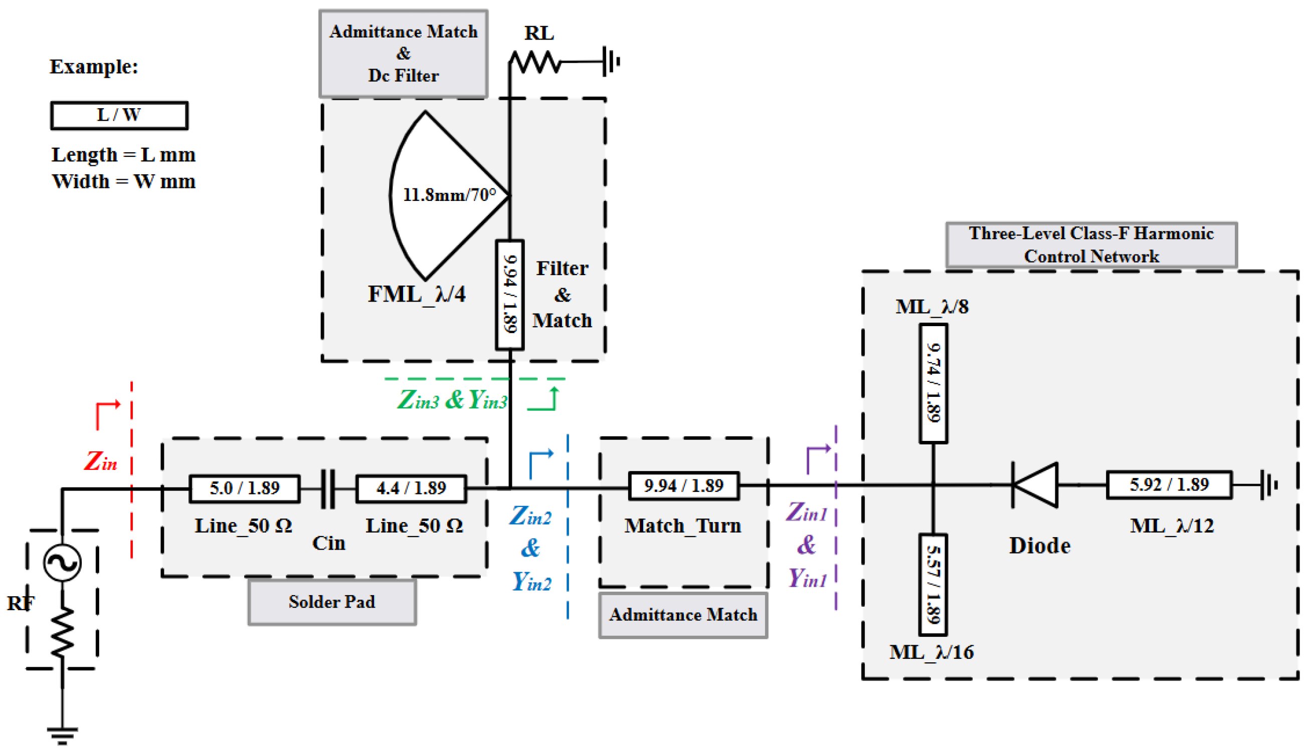
Figure 1. The schematic of the High Power Rectifier.
Electronics 14 04461 g001
Figure 2. The design of admittance matching: (a) The input impedance. (b) Parallel equivalent circuit of impedance. (c) Admittance Parallel Equivalent Circuit.
Electronics 14 04461 g002
Figure 3. Proposed high-power rectifier: (a) Layout; (b) Fabricated circuit.
Electronics 14 04461 g003
Figure 4. The measuring environment of a high-power rectifier.
Electronics 14 04461 g004
Figure 5. Simulation and measurement Efficiency (a) Power Variation. (b) Frequency Variation. (c) Load Variation.
Electronics 14 04461 g005
Table 1. Comparison of rectifiers with high-power performance comparison of high-power rectifier circuits.
Ref.Freq. (GHz)Pin (dBm)Efficiency (%)Diode ModelDiode BV (V)
[21]0.4333078.9HSMS-282P156
[23]5.83471Ga N164
[24]2.453366.8HSMS-282P15
[20]2.453074.4HSMS-282015
[19]2.453069.4HSMS-270P25
[25]2.454061.1HSMS-270C25
This work2.5532.576.9HSMS-270B25
Disclaimer/Publisher’s Note: The statements, opinions and data contained in all publications are solely those of the individual author(s) and contributor(s) and not of MDPI and/or the editor(s). MDPI and/or the editor(s) disclaim responsibility for any injury to people or property resulting from any ideas, methods, instructions or products referred to in the content.