Article

Investigation of Reliability Strengthening by Six-Sided Protective Structure in Fan-Out Wafer-Level Packaging

1
China Electronics Technology Group Corporation 58th Research Institute, Wuxi 214122, China
2
School of Materials, Shenzhen Campus of Sun Yat-sen University, Shenzhen 518107, China
3
Guangdong Provincial Key Laboratory of Magnetoelectric Physics and Devices, School of Physics, Sun Yat-sen University, Guangzhou 510275, China
*
Authors to whom correspondence should be addressed.
These authors contributed equally to this work.
Electronics 2025, 14(22), 4429; https://doi.org/10.3390/electronics14224429
Submission received: 5 October 2025 / Revised: 11 November 2025 / Accepted: 11 November 2025 / Published: 13 November 2025
(This article belongs to the Section Industrial Electronics)

Abstract

In this study, the reliability differences between a normal structure and a six-sided protective structure are investigated for 300 mm fan-out wafer-level packaging. Theoretical analysis indicates that the six-sided protective structure exhibits lower thermal stress (dropping by 9.06%) and superior thermal stability. The introduced epoxy molding compound (EMC) protective layer bonds tightly with other layers without changing the performance of the solder balls, such as shear strength and failure modes. After reliability testing, all the normal structure samples passed the high accelerated stress test (HAST) and temperature cycling testing (TCT), but none passed the pressure cooking testing (PCT). By contrast, the six-sided protective structure samples passed all tests. Scanning acoustic microscopy and cross-sectional scanning electron microscopy (SEM) pictures further confirmed that the six-sided protective structure passed the PCT. This result indicates that the reliability of the six-sided protective structure has been strengthened, consistent with the simulation analysis. A packaging solution for enhancing reliability by reducing structural thermal stress has been suggested.

1. Introduction

As Moore’s Law approaches its physical limits, the semiconductor industry is increasingly relying on advanced packaging technologies to meet the demand for higher performance, smaller size, and lower power consumption in electronic products [1,2,3,4,5,6]. According to the layout of the redistribution layer, advanced packaging technology can be divided into two categories: fan-in wafer-level packaging and fan-out wafer-level packaging. The redistribution layer of fan-in wafer-level packaging is set inside the chip, while fan-out wafer-level packaging allows the redistribution layer to extend beyond the edge of the chip. The more flexible redistribution layer design has made fan-out wafer-level packaging attract more and more attention [7,8,9,10].
In a normal fan-out wafer-level packaging (FOWLP) structure, the back side and four sidewalls of the chip are encapsulated by EMC, while the front surface is covered by a redistribution layer (Figure 1a). Due to the nature of fan-out wafer-level packaging, its reliability hinges upon the ability of the different layers within the package to absorb the shock and mechanical stress generated by the differing coefficients of thermal expansion (CTE) of the various materials [11,12,13,14,15,16]. Lin et al. researched the impact of CTE mismatch on structural reliability in fan-out packaging, demonstrating that CTE mismatch may cause device warping and generate mechanical stresses that induce cracking in the redistribution layer [17]. Che et al. investigated the solder ball reliability under temperature cycling testing (TCT). The results showed that low CTE underfill helps improve solder ball reliability [18].
To obtain higher long-term reliability, a novel and highly attractive wafer-level packaging technology—the six-sided protective structure (Figure 1b)—has emerged [19]. In 2015, UTAC proposed a six-sided protection structure, where the four side walls and the front of the chip are protected by molding, and the back of the chip is protected by a laminated film [20]. Similarly, Huatian Technology employed a back-molding process to achieve six-sided protection. Some researchers have studied the six-sided protective structures [21]. Lau et al. investigated the average lifetime, failure locations, and failure modes of solder joints within a six-sided protective structure under TCT (−55–125 °C, 50-min cycle) [22]. Qin et al. researched the warping evolution of the six-sided protective structure during different manufacturing processes and proposed corresponding warping control methods [23]. The manufacturing processes for six-sided protective structures have been extensively studied, yet comprehensive reliability studies are still needed. Investigating the reliability differences between different structures and their mechanisms will help further enhance the reliability of FOWLP.
In this study, we demonstrate a six-sided protective structure employing a re-molding process. Following the initial encapsulation, the rear and all four sides of the chip are protected by epoxy molding compound (EMC). Subsequently, a second encapsulation process provides complete protection for the front-side redistribution layer of the chip. Thermal stress analysis indicates that the six-sided protective structure exhibits lower thermal stresses than the normal structure, implying superior structural stability. The performance of the solder balls and the encapsulation effect are investigated by the techniques, including cross-sectional scanning electron microscopy (SEM) and shear force testing. Reliability test results indicate that this structure exhibits superior resistance to delamination caused by humid and hot conditions compared to conventional normal structures. This paper demonstrates that we have provided a simple but efficient way to enhance the reliability of fan-out packaging products.

2. Materials and Methods

2.1. FOWLP Device

The normal structure FOWLP device and the six-sided protective structure FOWLP device were produced by China Electronics Technology Group Corporation, 58th Research Institute. The microstructure of the FOWLP devices was investigated using an SEM machine (Sigma 500, Carl Zeiss AG, Oberkochen, Germany).

2.2. Shear Test

The FOWLP devices were subjected to shear force measurement using a shear force testing machine (Dage 4800 Optima, Nordson DAGE, Cleveland, OH, USA). The height of the knife lifting and its shear speed are fixed, with the height of the knife lifting being 10 μm and the shear speed being 20 μm/s. After fixing the device, push the solder ball along a direction parallel to the device until separation occurs, and record the shear force values under each parameter condition.

2.3. Reliability Test

The FOWLP devices were subjected to high accelerated stress test (HAST), pressure cooking testing (PCT), and TCT, respectively. The HAST conditions are 130 °C, 85% RH, duration 96 h. The PCT conditions are 121 °C, 100% RH, duration 96 h. And the TCT conditions are −65~150 °C, 1000 cycles. After the reliability test, these samples were removed to examine the shear force and morphology.

2.4. Finite Element Simulation

This model is conducted with the help of the COMSOL Multiphysics® 6.2 in-built tools. The geometry consists of two-dimensional solid rectangular blocks. We primarily use a two-dimensional “Solid Mechanics” interface for modeling to simulate its thermal expansion characteristics. We also set the transverse temperature boundaries to be periodic, ensuring that each temperature value on both boundaries is equal. We utilize the predefined multiphysics coupling and steady-state study of “Conjugate Heat Transfer” to establish the simulation, mimicking natural convection. We set the heat dissipation rate Q per unit volume in the solid to simulate the heating of the Si region under actual conditions. Specific material parameters are shown in Table 1.

3. Results and Discussion

3.1. Packaging Structure Observations

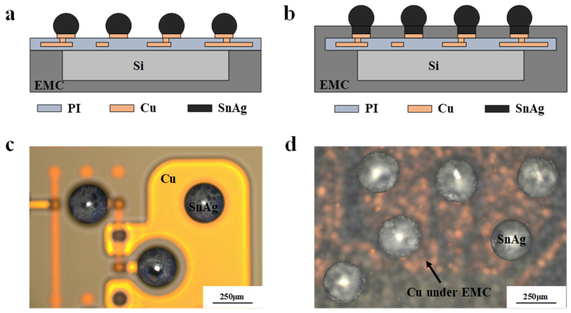
Figure 2a shows the normal structure. The chip is embedded within the EMC, with its front surface exposed. Two passivation layers and two redistribution layers are alternately arranged on the front surface of the chip, and solder balls are interconnected with the redistribution layers. The six-sided protective structure is shown in Figure 2b. By contrast, an additional EMC layer covers the surface and surrounding side walls of the redistribution layer. And the solder balls interconnect with the redistribution layer via bumps that traverse the EMC layer. Figure 2c,d demonstrate the top view of the redistribution layer in the two packaging structures. It can be seen that the redistribution layer in normal structures is directly observable, whereas in six-sided protective structures, the redistribution layer (RDL) is covered by the EMC and is no longer clearly visible. Such a design can offer a degree of protection to the redistribution layer, reducing performance degradation caused by surface scratches and other damage.

3.2. Structural Reliability Analysis

A two-dimensional finite element model was constructed using COMSOL Multiphysics to analyze the reliability of two packaging structures. This finite element model, incorporating aspects of solid, fluid, and heat transfer properties, can quantify the thermal stresses generated in various packaging structures and provide temperature and stress distributions to illustrate structural stability [24,25,26,27]. We first performed a thermal stress analysis on the package structure during a temperature ramp from −50 °C to 150 °C, maintaining a consistent temperature throughout the structure. Using the “Solid Mechanics” Mode, add a built-in multiphysics “Thermal Expansion” node under the “Linear Elastic Material” subnode. “Rigid motion suppression” was used to constrain the package structure, and a periodic condition along the x-direction was added. Finally, the steady-state results were calculated.
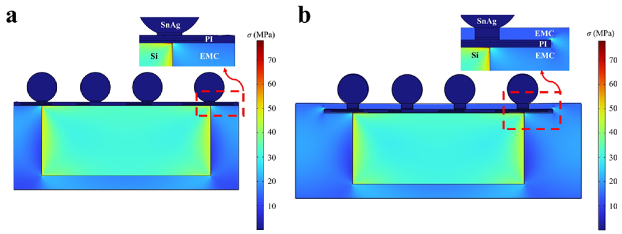
Setting room temperature (20 °C) as the base temperature for the package structure, no thermal stress is generated within the structure. Figure 3 shows the thermal stress generated by the two package structures at 100 °C. Simulation results show that the thermal stress generated in the Si region is significantly higher than that in the external region, and the thermal stress at the interfaces of different materials, especially at sharp points, is much greater than that in the remaining smooth areas. The maximum stress is at the four corners of the rectangular area where the Si is located. At 100 °C, the maximum thermal stresses of normal structure and six-sided protective structure are 80.2 MPa and 78.6 MPa, respectively. Within the range of −50–150 °C, the maximum thermal stress of the normal structure is 2.01% higher than that of the six-sided protective structure. These findings indicate that at the same temperature, the thermal stress of the six-sided protective structure is lower than that of the normal structure, implying superior structural stability.
Reliability analysis of the two structures was conducted under air convection. A two-dimensional coupled model—integrating solid mechanics, heat transfer in solids and fluids, and laminar flow—was employed to analyze thermally induced stresses in the presence of convection [28]. The Si region was set as a heat source, generating heat from the Si, causing the entire structure to heat up. Different power levels were set to change the temperature of the structure. Air circulation areas were set at the top and bottom of the package structure to force air flow to dissipate heat from the package structure. The model makes use of the “Conjugate Heat Transfer” predefined multiphysics coupling with a stationary study to set up the simulation. The external air temperature and flow velocity are given, and temperature continuity is applied to all interior boundaries. Due to heating of the fluid, deviations occur in the local density, ρ, compared to the inlet density, ρ0. This results in a local buoyancy force defined using the “Gravity” feature in the “Single Phase Flow” interface.
Figure 4 shows multiple results for a heat source with a heating power of 2 × 10⁶ W/m3. In Figure 4a,d, the initial air velocity is 0.01 m/s, the initial temperature is 20 °C, and the air flow is laminar. Figure 4b,e show the temperature distribution of the normal structure and the six-sided protective structure. Clearly, at the same heating power, the temperature of the six-sided protective structure is slightly lower than that of the normal structure. The average temperature of the Si wafer region in the normal structure is 88.56 °C, while that in the six-sided protective structure is 88.74 °C, a temperature drop of 0.94%. Figure 4c,f show the distribution of thermal stress. Currently, the average stresses of normal structure and six-sided protective structure are 16.4 MPa and 15.0 MPa, respectively, with the average stress of the six-sided protective structure dropping by 9.06%. These results indicate that a six-sided protective structure has higher heat dissipation performance and greater structural reliability.
Figure 5a,b show the temperature and thermal stress variations for the normal structure and the six-sided protective structure. Figure 4a shows the average thermal stress variation trend under heating and cooling conditions from −50 °C to 150 °C. The stress varies linearly with temperature, based on a given temperature. Within this temperature range, the thermal stress of the six-sided protective structure decreases by 7.85% compared with the normal structure, and the stress change rate does not change with temperature. Figure 5b shows the temperature and average thermal stress variations for the entire package within the Si region’s heating power range of 0–3.5 × 10⁶ W/m3. As the heating power increases, the temperature and thermal stress of the six-sided protective structure decrease more significantly compared to the normal structure. At a power of 3.5 × 10⁶ W/m3, the temperature of the six-sided protective structure decreases by 1.21%, and the average thermal stress decreases by 9.17%. A thicker stress buffer layer would enhance reliability [29]. In the six-sided protective structure, the upper protective layer for the front-side RDL acts as a stress buffer layer. The thickness of the upper protective layer affects the protective performance. The specific data is shown in Figure 5c. The thermal stress of the overall structure decreases linearly with the increase in the thickness of the upper layer. As the thickness of the upper layer increased from 20 µm to 60 µm, the thermal stress decreased by 2.57%. Compared to normal structures, the introduction of an additional EMC layer can reduce internal stresses arising from CTE mismatch, thereby enhancing reliability.
During finite element simulation, it was found that the convergence of the structure is very low in sensitivity to mesh density. As the element size is gradually reduced, key output quantities (such as stress, strain, and displacement) exhibit extremely strong stability, indicating that the numerical solution has converged to the neighborhood of the true solution. This also demonstrates that the mesh density is sufficient, and the calculation results are reliable. During the mesh refinement process, the difference in thermal stress data between the coarsest and finest meshes used was only 0.0094%, as shown in Figure 5d.
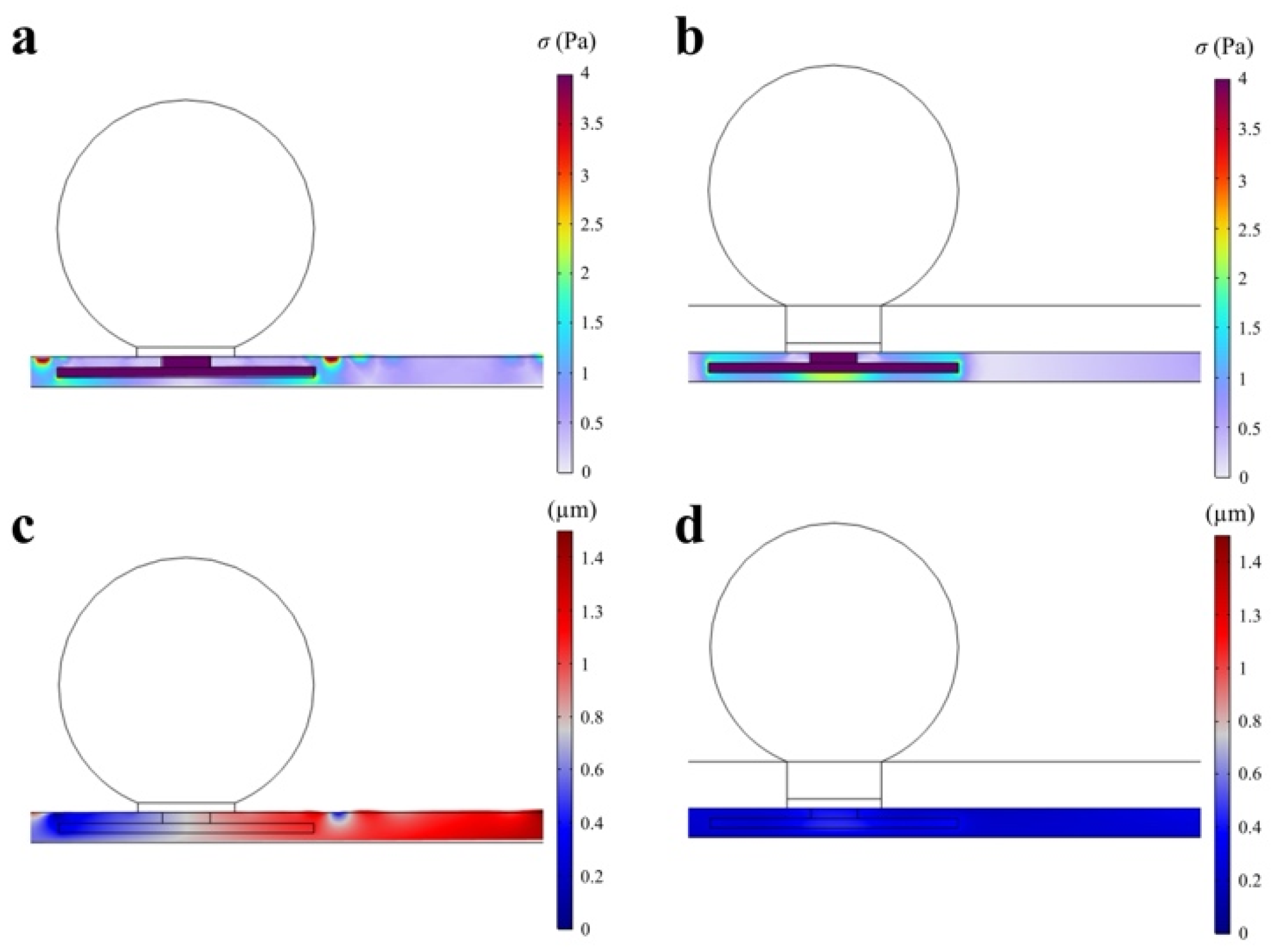
In the stress concentration zones, the stress in the six-sided protective structure is uniformly distributed around the electrode. In contrast, the stress in the normal structure diffuses from the electrode to the interior and surface of the PI layer. The stress distribution in the normal structure is uneven, and the maximum stress value is much greater than that in the six-sided protective structure, as shown in Figure 6a,b. Furthermore, due to the lack of a protective layer, the PI layer in the normal structure exhibits significant upward warping, reaching an amplitude of 1.5 µm, while the PI layer in the six-sided protective structure shows almost no deformation, as shown in Figure 6c,d. This demonstrates that the hexagonal protective structure possesses superior thermal stability.

3.3. Solder Ball Performance

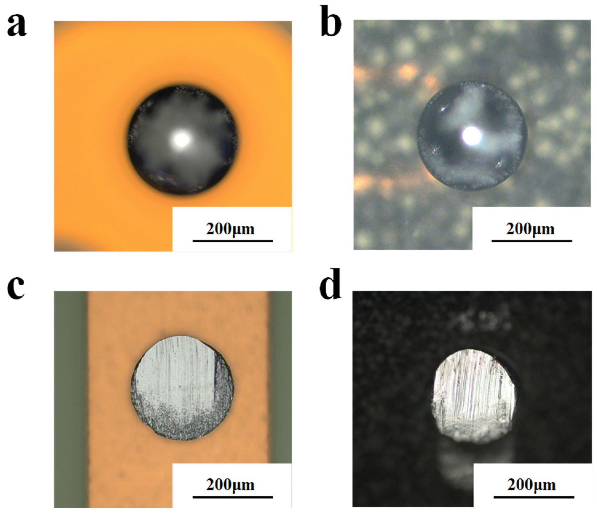
To get more details about the six-sided protective structure, we analyzed the performance of the solder balls. Figure 7a,b shows the top view of solder balls in both the normal structure and the six-sided protective structure. There is no discernible difference in the appearance of the solder balls between the two structures. This indicates that the introduced EMC layer has not affected the formation of the solder balls. Furthermore, we adopted shear force testing to evaluate the mechanical strength of the solder balls [30,31]. Lower knife lifting height and faster shear speed would result in higher ball shear strength. Therefore, the height of the knife lifting and its shear speed are fixed, with the height of the knife lifting being 10 μm and the shear speed being 20 μm/s. For each testing condition, shear 25 solder balls and record the corresponding shear force (Table 2). A solder ball shear force value exceeding 3.9 mg/μm2 is deemed acceptable. It can be seen that the shear force values of the solder balls meet specifications in both structures. It is well known that in shear force tests, the majority of failures occur near the pad surface, but the acceptable fracture location is within the solder ball itself. Figure 7c,d illustrates the failure modes of the two structures. The fracture location is inside the solder ball, with a smooth fracture surface. This means the solder ball exhibits good bonding to the redistribution layer, and the mechanical strength is acceptable.

3.4. Microscopic Morphology

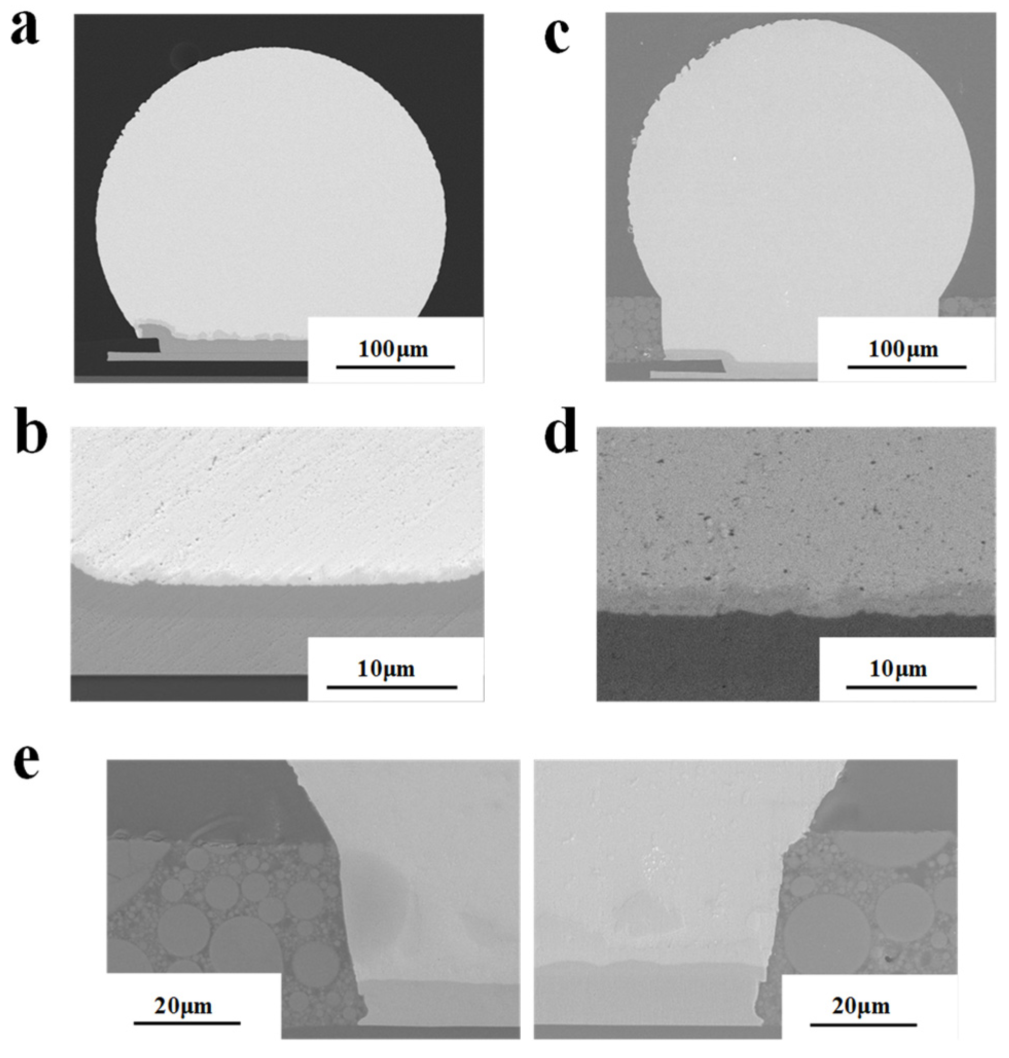
The microstructure of the packaging structure was investigated using cross-sectional SEM. In normal structures, solder balls are uniformly dense and rounded, with an intermetallic compound (IMC) layer that is compact and measures between 0.5 μm and 1.4 μm in thickness (Figure 8a,b). Similar microstructures were also observed in the six-sided encapsulation structure, with an IMC layer thickness ranging from 0.7 μm and 1.6 μm (Figure 8c,d). Owing to the characteristics of the six-sided protective structure, the solder balls are partially embedded within the EMC. Consequently, we measured the bonding state between the solder balls and the EMC. From Figure 8e, we can clearly observe the interface between the solder ball and the EMC, which exhibits a tight bond with no delamination. The results above indicate that the solder ball performance remains acceptable after introducing an EMC layer for surface protection within the packaging structure.
The six-sided protective structure achieves all-around protection for the redistribution layer by incorporating an EMC layer on top of the normal structure. The cross-sectional SEM image, as shown in Figure 9, reveals each interface associated with the EMC layer to be clearly discernible. The interface between the EMC and the redistribution layer is tightly integrated without separation, and the same is observed between EMC layers. The additional EMC protection layer is beneficial for enhancing reliability.

3.5. Reliability Results

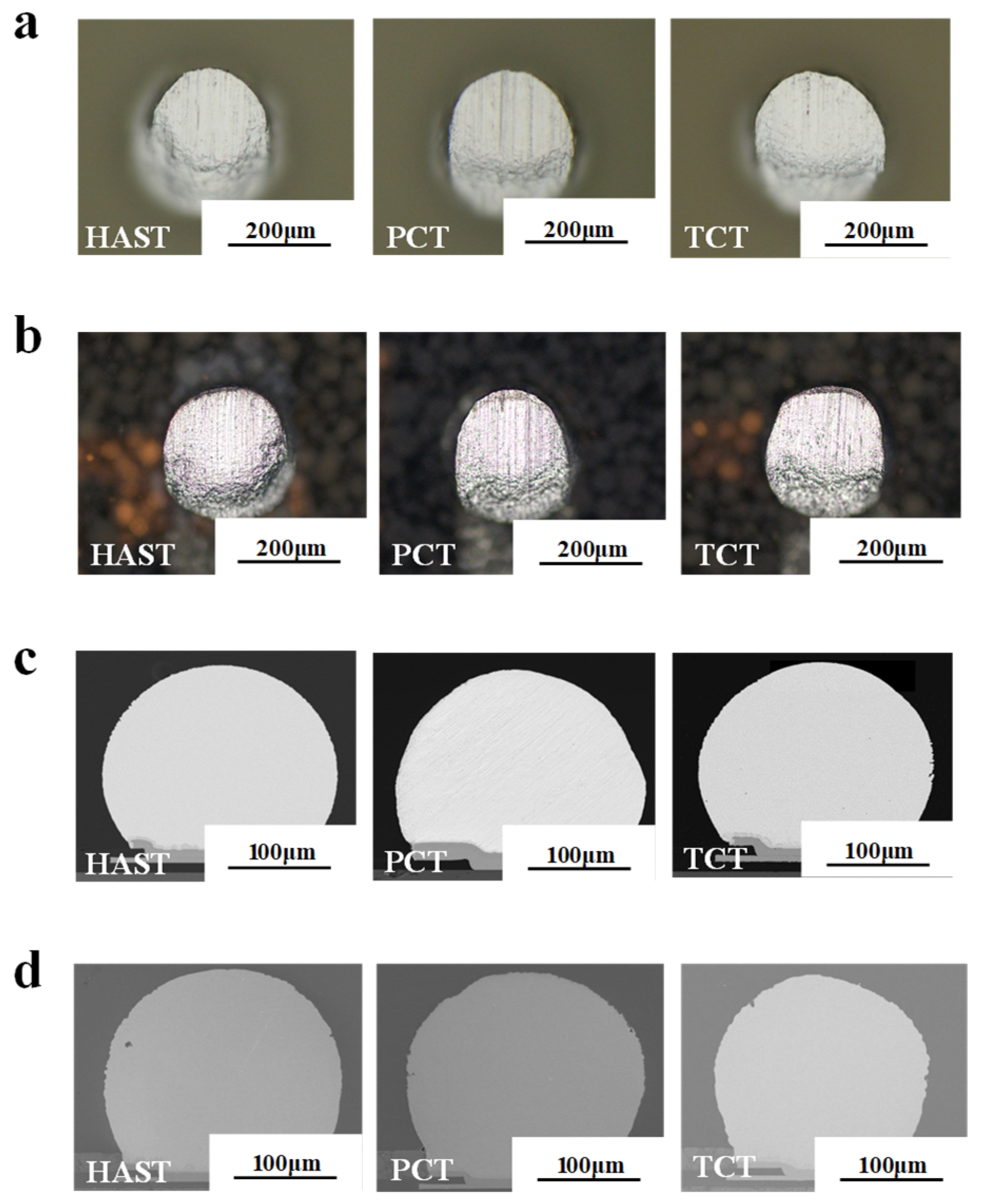
To elucidate the contribution of EMC to enhancing reliability performance, we designed reliability tests related to humidity and heat. Following the sample pre-treatment, HAST, PCT, and TCT were conducted, respectively. We employed shear force testing and SEM to investigate the reliability differences between normal structures and six-sided protective structures. After the reliability test ended, shear 25 solder balls and record the corresponding shear force (Table 3). It can be observed that the shear force of the solder balls in both structures has decreased slightly [32], but remains within an acceptable range. Moreover, compared to the normal structure, both the minimum value in the TCT and the average value in the PCT are slightly lower in the six-sided protective structure. This may be related to the uniformity of solder ball preparation, as shear force values are influenced by temperature fluctuations [33]. Solder ball formation is performed through wafer-level reflow. During the reflow process, temperature variations across different regions of the wafer cause differences in the reflow temperature profiles of the solder balls, which consequently affect the shear force values. The failure modes of solder balls before and after reliability testing were similar, with fractures located inside the solder balls (Figure 10a). The SEM image of the solder ball after reliability testing is shown in Figure 10c. In the normal structure, the IMC layer remains in a dense state, though its thickness has increased slightly. The same phenomenon occurs in the six-sided protective structure, with the corresponding failure modes and SEM images shown in Figure 10b,d, respectively.
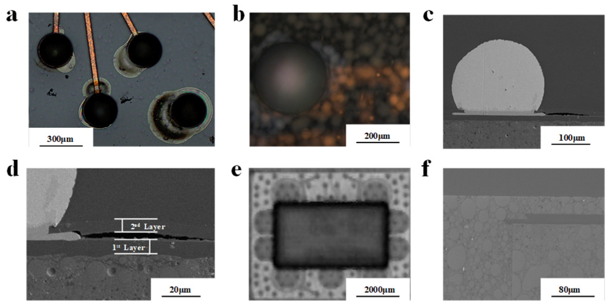
Then we turn to study the reliability difference in encapsulation structures. The reliability test results are shown in Table 4. Under the same testing conditions, both structures were evaluated using the same number of samples. In the normal structure, all samples passed the HAST and TCT, but none passed the PCT. By contrast, the six-sided protective structure passed all reliability tests. Figure 11a,b show the top view of the two packaging structures after finishing the reliability tests. In the normal structure, when the PCT finished, circular protrusions appeared on the sample surface, whereas no changes were observed on the sample surface after the other reliability tests ended. The cross-sectional SEM image indicates that delamination has occurred at this location, which also means that the test has not been passed (Figure 11c,d). However, in the six-sided protective structure, no significant changes were found on the sample surface at the end of the reliability testing. Owing to the presence of the EMC layer, it is not possible to clearly observe morphological changes within the packaging structure. Scanning acoustic microscopy and cross-sectional SEM were employed to further investigate the internal morphology of the six-sided protective structure. Ultrasonic scanning can detect defects such as delamination, cracks, and voids within internal structures [34,35]. As shown in Figure 11e, no delamination was detected within any of the samples. The SEM images also reveal that no delamination has occurred at the interfaces associated with the ECM and the redistribution layer (Figure 11f). The results above indicate that a six-sided protective structure offers superior reliability compared to the normal structure, consistent with simulation results.

4. Conclusions

In conclusion, we investigated the reliability differences between a normal structure and a six-sided protective structure in 300 mm fan-out wafer-level packaging. The key metrics for the two structures are shown in Table 5. Thermal stress simulation results indicate that as temperature increases from 20 °C to 100 °C, the six-sided protective structure exhibits lower thermal stress, with a reduction of 9.06%. And at a power of 3.5 × 10⁶ W/m3, the average thermal stress of the six-sided protective structure decreases by 9.17%. Reduced thermal stress indicates that the packaging structure possesses greater capacity to absorb shocks and stresses generated by CTE mismatch, thereby delivering superior reliability. This simulation demonstrates that the six-sided protective structure offers superior structural stability. The introduction of an EMC protective layer within the normal structure did not result in any significant change to the shear force or failure mode of the solder balls. Morphological analysis indicates that the EMC protective layer exhibits tight bonding with both the redistribution layer, the solder ball, and the EMC material, with no delamination. In addition, the reliability measurement indicates that the normal structure passed the HAST and TCT. However, with the occurrence of delamination, the pass rate for PCT has dropped to 0%. By contrast, the six-sided protective structure successfully passed all reliability tests with a 100% pass rate. Ultrasonic scanning and morphological analysis further confirmed the reliability test results. The above results indicate that the reliability of the six-sided protective structure has been strengthened, consistent with the simulation analysis. It means that reducing structural thermal stresses is an effective solution for enhancing the reliability of FOWLP.

Author Contributions

C.Y.: Writing—original draft, Visualization, Validation, Methodology, Investigation, Conceptualization. J.T.: Thermal stress simulation, Methodology, Simulation part writing. W.T.: Investigation, Methodology. F.D.: Methodology, Conceptualization. Y.J.: Resources. W.C.: Writing—review, Methodology, Conceptualization. C.W.: Writing—review and editing, Supervision, Resources, Funding acquisition, Methodology, Conceptualization. All authors have read and agreed to the published version of the manuscript.

Funding

This work was supported by the National Key Research and Development Program of China under Grant 2024YFF1400200, and the Jiangsu Province Innovation Support Program (Soft Science Research) Special Fund under Grant BK20243020.

Data Availability Statement

The original contributions presented in this study are included in the article. Further inquiries can be directed to the corresponding authors.

Conflicts of Interest

Authors Cheng Yang, Wenxue Tang, Feihu Dai, Yong Ji, and Chengqian Wang were employed by the company China Electronics Technology Group Corporation 58th Research Institute. The remaining authors declare that the research was conducted in the absence of any commercial or financial relationships that could be construed as a potential conflict of interest.

References

  1. Qu, S.; Liu, Y. Wafer-Level Chip-Scale Packaging; Springer: New York, NY, USA, 2015; pp. 54–64. [Google Scholar] [CrossRef]
  2. Shi, L.; Chen, L.; Zhang, D.W.; Liu, E.; Liu, Q.; Chen, C.-I. Improvement of thermo-mechanical reliability of wafer-level chip scale packaging. J. Electron. Packag. 2018, 140, 011002. [Google Scholar] [CrossRef]
  3. Liu, P.; Wang, J.; Tong, L.; Tao, Y. Advances in the fabrication processes and applications of wafer level packaging. J. Electron. Packag. 2014, 136, 024002. [Google Scholar] [CrossRef]
  4. Arriola, E.R.; Ubando, A.T.; Gonzaga, J.A.; Lee, C.-C. Wafer-level chip-scale package lead-free solder fatigue: A critical review. Eng. Fail. Anal. 2023, 144, 106986. [Google Scholar] [CrossRef]
  5. Cao, L.; Lee, T.C.; Chen, R.; Chang, Y.-S.; Lu, H.; Chao, N.; Huang, Y.-L.; Wang, C.-C.; Huang, C.-Y.; Kuo, H.-C.; et al. Advanced fanout packaging technology for hybrid substrate integration. In Proceedings of the 2022 IEEE 72nd Electronic Components and Technology Conference (ECTC), San Diego, CA, USA, 31 May–3 June 2022; pp. 1362–1370. [Google Scholar]
  6. Hsu, F.C.; Lin, J.; Chen, S.M.; Lin, P.Y.; Fang, J.; Wang, J.H.; Jeng, S.P. 3D heterogeneous integration with multiple stacking fan-out package. In Proceedings of the 2018 IEEE 68th Electronic Components and Technology Conference (ECTC), San Diego, CA, USA, 29 May–1 June 2018; pp. 337–342. [Google Scholar]
  7. Lau, J.H. Recent advances and trends in fan-out wafer/panel-level packaging. J. Electron. Packag. 2019, 141, 040801. [Google Scholar] [CrossRef]
  8. Lau, J.H.; Li, M.; Li, Q.M.; Xu, I.; Chen, T.; Li, Z.; Tan, K.H.; Yong, Q.X.; Cheng, Z.; Wee, K.S.; et al. Design, materials, process, fabrication, and reliability of fan-out wafer-level packaging. IEEE Trans. Compon. Packag. Manuf. Technol. 2018, 8, 991–1002. [Google Scholar] [CrossRef]
  9. Braun, T.; Becker, K.-F.; Voges, S.; Thomas, T.; Kahle, R.; Bader, V.; Bauer, J.; Aschenbrenner, R.; Lang, K.-D. Challenges and opportunities for fan-out panel level packing (FOPLP). In Proceedings of the 2014 9th International Microsystems, Packaging, Assembly and Circuits Technology Conference (IMPACT), Taipei, Taiwan, 22–24 October 2014; pp. 154–157. [Google Scholar]
  10. Chen, D.-L.; Hu, I.; Chen, K.Y.; Shih, M.-K.; Tarng, D.; Huang, D.; On, J. Material and structure design optimization for panel-level fan-out packaging. In Proceedings of the 2019 IEEE 69th Electronic Components and Technology Conference (ECTC), Las Vegas, NV, USA, 28–31 May 2019; pp. 1710–1715. [Google Scholar]
  11. Rongen, R.; Roucou, R.; Wel, P.V.; Voogt, F.; Swartjes, F.; Weide-Zaage, K. Reliability of wafer level chip scale packages. Microelectron. Reliab. 2014, 54, 1988–1994. [Google Scholar] [CrossRef]
  12. Chen, C.C.; Chen, K.H.; Wu, Y.S.; Tsao, P.H.; Leu, S.T. WLCSP solder ball interconnection enhancement for high temperature stress reliability. In Proceedings of the 2020 IEEE 70th Electronic Components and Technology Conference (ECTC), Orlando, FL, USA, 3–30 June 2020; pp. 1212–1217. [Google Scholar]
  13. Lau, J.; Li, M.; Lei, Y.; Li, M.; Xu, I.; Chen, T.; Yong, Q.X.; Cheng, Z.; Kai, W.; Lo, P.; et al. Reliability of fan-out wafer-level heterogeneous integration. International Symposium on Microelectronics. Int. Microelectron. Assem. Packag. Soc. 2018, 2018, 224–232. [Google Scholar]
  14. Cardoso, A.; Martins, S.; Gouvea, A. Characterization of electromigration effects in rdl of wafer level fan-in and fan-out packaging using a novel analysis approach. In Proceedings of the 2018 7th Electronic System-Integration Technology Conference (ESTC), Dresden, Germany, 18–21 September 2018; pp. 1–7. [Google Scholar]
  15. Hou, F.; Lin, T.; Cao, L.; Liu, F.; Li, J.; Fan, X.; Zhang, G.Q. Experimental verification and optimization analysis of warpage for panel-level fan-out package. IEEE Trans. Compon. Packag. Manuf. Technol. 2017, 7, 1721–1728. [Google Scholar] [CrossRef]
  16. Yu, C.K.; Chiang, W.S.; Liu, N.W.; Lin, M.Z.; Fang, Y.H.; Lin, M.J.; Lin, B.; Huang, M. A unique failure mechanism induced by chip to board interaction on fan-out wafer level package. In Proceedings of the 2017 IEEE International Reliability Physics Symposium (IRPS), Monterey, CA, USA, 2–6 April 2017; pp. 4A-6.1–4A-6.4. [Google Scholar]
  17. Lin, R.; Yip, L.; Lai, C.; Lin, B.-Y.; Peng, C.; Syu, C.; Chang, M. Reliability Challenges of Large Organic Substrate with High-Density Fan-out Package. In Proceedings of the 2023 IEEE 73rd Electronic Components and Technology Conference (ECTC), Orlando, FL, USA, 30 May–2 June 2023; pp. 277–282. [Google Scholar]
  18. Che, F.X. Study on board level solder joint reliability for extreme large fan-out WLP under temperature cycling. In Proceedings of the 2016 IEEE 18th Electronics Packaging Technology Conference (EPTC), Singapore, 30 November–3 December 2016; pp. 207–212. [Google Scholar]
  19. Lau, J.H.; Ko, C.-T.; Peng, C.-Y.; Tseng, T.-J.; Yang, K.-M.; Xia, T.; Lin, P.B.; Lin, E.; Chang, L.; Liu, H.N.; et al. Reliability of 6-side molded panel-level chip-scale packages (PLCSPs). In Proceedings of the 2021 IEEE 71st Electronic Components and Technology Conference (ECTC), San Diego, CA, USA, 1 June–4 July 2021; pp. 885–894. [Google Scholar]
  20. Smith, L.; Dimaano, J., Jr. Development approach & process optimization for sidewall WLCSP protection. In Proceedings of the 12th Annual International Wafer-Level Packaging Conference (IWLPC), San Jose, CA, USA, 12–14 October 2015; pp. 1–4. [Google Scholar]
  21. Ma, S.; Wang, T.; Xiao, Z.; Yu, D. Process development of five-and six-side molded WLCSP. In Proceedings of the 2018 China Semiconductor Technology International Conference (CSTIC), Shanghai, China, 11–12 March 2018; pp. 1–3. [Google Scholar]
  22. Lau, J.H.; Ko, C.-T.; Peng, C.-Y.; Tseng, T.-J.; Yang, K.-M.; Xia, T.; Lin, P.B.; Lin, E.; Chang, L.; Liu, H.N.; et al. Thermal cycling test and simulation of six-side molded panel-level chip-scale packages (PLCSPs). J. Microelectron. Electron. Packag. 2021, 18, 67–80. [Google Scholar] [CrossRef]
  23. Qin, F.; Zhao, S.; Dai, Y.; Yang, M.; Xiang, M.; Yu, D. Study of warpage evolution and control for six-side molded WLCSP in different packaging processes. IEEE Trans. Compon. Packag. Manuf. Technol. 2020, 10, 730–738. [Google Scholar] [CrossRef]
  24. Yip, L.; Lin, R.; Lai, C.; Peng, C. Reliability challenges of high-density fan-out packaging for high-performance computing applications. In Proceedings of the 2022 IEEE 72nd Electronic Components and Technology Conference (ECTC), San Diego, CA, USA, 31 May–3 June 2022; pp. 1454–1458. [Google Scholar]
  25. Lee, Y.-C.; Lai, W.-H.; Hu, I.; Shih, M.-K.; Kao, C.-L.; Tarng, D.; Hung, C.-P. Fan-out chip on substrate device interconnection reliability analysis. In Proceedings of the 2017 IEEE 67th Electronic Components and Technology Conference (ECTC), Orlando, FL, USA, 30 May–2 June 2017; pp. 22–27. [Google Scholar]
  26. Fan, Y.; Tian, S.; Jiao, H.; Meng, D.; Wang, Z.; Meng, M. Interconnect Reliability Simulation Analysis of Fan-out Package redistribution Layer. In Proceedings of the 2023 8th International Conference on Integrated Circuits and Microsystems (ICICM), Nanjing, China, 20–23 October 2023; pp. 98–104. [Google Scholar]
  27. Zhang, L.; Sun, L.; Han, J.-G.; Guo, Y.-H. Reliability of lead-free solder joints in WLCSP device with finite element simulation and Taguchi method. Int. J. Nonlinear Sci. Numer. Simul. 2014, 15, 405–410. [Google Scholar] [CrossRef]
  28. Wang, P.H.; Huang, A.; Chiang, K.N. Design and reliability assessment of stacked fan-out packaging. In Proceedings of the 2018 Pan Pacific Microelectronics Symposium (Pan Pacific), Big Island, HI, USA, 5–8 February 2018; pp. 1–6. [Google Scholar]
  29. Shih, M.-K.; Lee, Y.-C.; Chen, R.; Tarng, D.; Hung, C.P. Parameters study of thermomechanical reliability of board-level fan-out package. In Proceedings of the 2017 International Conference on Electronics Packaging (ICEP), Yamagata, Japan, 19–22 April 2017; pp. 66–70. [Google Scholar]
  30. Zhang, S.; Duan, R.; Xu, S.; Xue, P.; Wang, C.; Chen, J.; Paik, K.-W.; He, P. Shear performance and accelerated reliability of solder interconnects for fan-out wafer-level package. J. Adv. Join. Process. 2022, 5, 100076. [Google Scholar] [CrossRef]
  31. Li, M.; Li, Q.; Lau, J.; Fan, N.; Kuah, E.; Kai, W.; Cheung, K.; Li, Z.; Tan, K.H.; Xu, I.; et al. Characterizations of fan-out wafer-level packaging. Int. Symp. Microelectronics. Int. Microelectron. Assem. Packag. Soc. 2017, 2017, 557–562. [Google Scholar] [CrossRef]
  32. Lau, J.H.; Lee, S.-W.R.; Chang, C. Solder joint reliability of wafer level chip scale packages (WLCSP): A time-temperature-dependent creep analysis. J. Electron. Packag. 2000, 122, 311–316. [Google Scholar] [CrossRef]
  33. Park, H.-P.; Seo, G.; Kim, S.; Ahn, K.-O.; Kim, Y.-H. Shear strength between Sn–3.0 Ag–0.5 Cu solders and Cu substrate after two solid-state aging processes for fan-out package process applications. J. Mater. Sci. Mater. Electron. 2019, 30, 10550–10559. [Google Scholar] [CrossRef]
  34. Zhu, J.; Ming, X.; Yao, X. Research on key process technology of RDL-first fan-out wafer level packaging. In Proceedings of the 2018 19th International Conference on Electronic Packaging Technology (ICEPT), Shanghai, China, 8–11 August 2018; pp. 309–313. [Google Scholar]
  35. Ke, C.Y.; Chen, L.P. The Simulation and Detection of Copper/Polyimide Delamination of Fan-Out Package Trace/Passivation Interface. In Proceedings of the 2021 International Conference on Electronics Packaging (ICEP), Tokyo, Japan, 12–14 May 2021; pp. 167–168. [Google Scholar]
Figure 1. Schematic diagram of (a) FOWLP structure and (b) new structure with six-sided protection.
Electronics 14 04429 g001
Figure 2. Schematic diagram of (a) normal structure and (b) six-sided protective structure. Top view of (c) normal structure and (d) six-sided protective structure.
Electronics 14 04429 g002
Figure 3. Thermal stress distribution of normal structure (a) and six-sided protective structure (b) at 100 °C.
Electronics 14 04429 g003
Figure 4. (a) Air flow velocity field, (b) Temperature distribution, (c) Stress distribution diagram of normal structure. (df) are the air flow velocity field, temperature distribution, and stress distribution of the six-sided protective structure, respectively.
Electronics 14 04429 g004
Figure 5. (a) Average stress variation of normal structure and six-sided protective structure in the range of −50 to 150 °C. (b) Changes in average temperature and average stress of the two structures under different heating powers. (c) The average stress variation of the thickness of the upper protective layer of the six-sided protective structure. (d) The average stress variation of mesh density.
Electronics 14 04429 g005
Figure 6. Stress concentration distribution in (a) normal structure and (b) six-sided protective structure; Deformation diagrams of (c) normal structure and (d) six-sided protective structure in the stress concentration zone.
Electronics 14 04429 g006
Figure 7. Top view of solder balls for normal structure (a) and six-sided protective structure (b). Failure modes of solder balls in normal structure (c) and six-sided protective structure (d).
Electronics 14 04429 g007
Figure 8. (a) Cross-section SEM images of a solder ball within the normal structure. (b) Cross-section SEM images of IMC within the normal structure. (c) Cross-section SEM images of a solder ball within the six-sided protective structure. (d) Cross-section SEM images of IMC within the six-sided protective structure. (e) Cross-section SEM images of the interface between the solder ball and the EMC within the six-sided protective structure.
Electronics 14 04429 g008
Figure 9. Cross-section SEM images of the interface within the six-sided protective structure.
Electronics 14 04429 g009
Figure 10. Failure modes in the normal structure (a) and six-sided protective structure (b) after reliability testing. Cross-section SEM images of a solder ball in the normal structure (c) and six-sided protective structure (d) after reliability testing.
Electronics 14 04429 g010
Figure 11. Top view of normal structure (a) and six-sided protective structure (b) after reliability testing. Cross-section SEM image (c) and enlarged image (d) of a solder ball in the normal structure after reliability testing. (e) An ultrasound scan image of the six-sided protective structure after reliability testing. (f) Cross-section SEM images of the interface within the six-sided protective structure after reliability testing.
Electronics 14 04429 g011
Table 1. Material parameters used in finite element simulation.
Materialsρ
kg/m3
α
10−6/C
E
MPa
k
W/mk
Poisson’s RatioC
J/(kg·K)
EMC20207.323,0000.30.23700
Si23342.6130,000186(−40)
135(25)
96(140)
0.28700
PI20005034000.40.341165
Cu900017120,0003930.35358
SnAg740021.650,00063.20.36222.1
Table 2. The shear forces of the two structures. Average values are calculated according to 25 solder balls.
StructureShear Force (mg/μm2)
Min.Max.Avg.STDEV
Normal structure5.46.45.70.27
Six-sided protective structure5.56.45.90.27
Table 3. The shear forces of the two structures after reliability testing. Average values are calculated according to 25 solder balls.
StructuresReliability TestsShear Force (mg/μm2)
Min.Max.Avg.STDEV
Normal structureHAST4.04.44.20.14
PCT4.04.54.30.15
TCT4.14.54.30.13
Six-sided protective structureHAST4.14.64.40.14
PCT4.04.54.20.15
TCT4.04.64.30.14
Table 4. The reliability results of the two structures.
StructuresReliability TestsNumber of Test Samples
TotalFailed
Normal structureHAST100
PCT1515
TCT150
Six-sided protective structureHAST100
PCT150
TCT150
Table 5. The key metrics for the two structures.
Key MetricsNormal
Structure
Six-Sided Protective StructureImprovement Value
Average thermal stress16.4 MPa15.0 MPa−9.06%
Average temperature88.56 °C88.74 °C−0.94%
HASTPassPass-
PCTFailPass100%
TCTPassPass-
Disclaimer/Publisher’s Note: The statements, opinions and data contained in all publications are solely those of the individual author(s) and contributor(s) and not of MDPI and/or the editor(s). MDPI and/or the editor(s) disclaim responsibility for any injury to people or property resulting from any ideas, methods, instructions or products referred to in the content.