Article

Ultra-Wideband Power Amplifier Using Non-Foster Characteristics of Coupled Transmission Lines

by
Hyeongjin Jeon
1,2,
Sooncheol Bae
1,
Kyungdong Bae
1,2,
Soohyun Bin
1,
Sangyeop Kim
1,
Yunhyung Ju
1,
Minseok Ahn
1,
Gyuhyeon Mun
1,
Keum Cheol Hwang
1,
Kang-Yoon Lee
1 and
Youngoo Yang
1,2,*
1
Department of Electrical and Computer Engineering, Sungkyunkwan University, 2066 Seobu-ro, Jangan-gu, Suwon-si 16419, Gyeonggi-do, Republic of Korea
2
para-PA Inc., 2066 Seobu-ro, Jangan-gu, Suwon-si 16419, Gyeonggi-do, Republic of Korea
*
Author to whom correspondence should be addressed.
Electronics 2025, 14(22), 4413; https://doi.org/10.3390/electronics14224413
Submission received: 24 October 2025 / Revised: 5 November 2025 / Accepted: 11 November 2025 / Published: 13 November 2025

Abstract

This paper presents a simplified matching network using coupled transmission lines (CTLs) for broadband power amplifiers. The proposed structure consists of a CTL with an electrical length shorter than λ /4 and a single shunt component, exhibiting excellent frequency characteristics across a wide bandwidth at both the input and load networks of the transistor. The reactance variation of the non-Foster elements in the equivalent circuit of the CTL with respect to frequency was analyzed, and the external reactive components were accordingly optimized to extend the bandwidth of the matching network. The proposed network was applied to the input and load networks of a GaN HEMT-based power amplifier. It was designed to maintain required performances over a wide frequency range of 1.9–4.9 GHz, covering both LTE and sub-6 GHz 5G bands, thereby achieving a fractional bandwidth (FBW) of 88.2%. The CTLs were fabricated on a two-layer printed-circuit board (PCB), and the additional shunt components were designed using surface-mount devices (SMDs). The overall power-amplifier module occupied a small area of 40 × 35 mm2. Using the continuous-wave (CW) signal, the proposed power amplifier exhibited a power gain of 10–14.8 dB and a drain efficiency (DE) of 47.5–60% at a saturated output power of 7.1–9.3 W across the entire operating frequency band. Using a 5G New Radio (NR) signal with a 100 MHz bandwidth and a peak-to-average power ratio (PAPR) of 7.8 dB, the amplifier achieved an average output power of 30 dBm, a DE of 20–27.5%, and an adjacent-channel leakage power ratio (ACLR) better than −30 dBc.

1. Introduction

In recent years, numerous broadband power amplifier (PA) design methodologies have been investigated to achieve wideband impedance matching and high efficiency over multiple octaves. Techniques such as resistive-reactive continuous modes [1], real-frequency synthesis-based distributed matching [2], quasi-class-J operation exploiting nonlinear output capacitance [3], fictitious matching networks [4], multi-frequency impedance mapping [5], and filter-based matching networks employing low-pass filter synthesis [6] have been successfully implemented. While these methods have extended the achievable bandwidth, they often rely on multiple transmission-line sections or frequency-dependent reactive elements, which increase circuit complexity and physical size. In addition, their impedance transformation characteristics strongly depend on the transistor’s intrinsic capacitance and the frequency-varying load terminations, leading to design sensitivity and performance degradation at the band edges. Moreover, most existing broadband PAs require intricate optimization of both input and output matching networks to simultaneously achieve gain flatness and efficiency enhancement. As a result, the trade-off between bandwidth, compactness, and design simplicity remains a major challenge in realizing highly integrated front-end modules for 5G and beyond wireless systems.
To address these limitations, this work introduces a new approach that applies the coupled transmission line (CTL) concept—originally explored for Doherty and harmonic-controlled amplifier architectures—to broadband PA design. Recent studies have also investigated CTL-based load networks for wideband and efficiency-enhanced Doherty architectures [7,8]. These works demonstrated that CTL structures can realize compact load networks with extended back-off ranges and that their inherent non-Foster characteristics can effectively reduce group delay and broaden the operating bandwidth [7,8]. Motivated by these insights, the present work applies the CTL principle not to Doherty architectures but to the broadband impedance matching of a single-stage PA, aiming to achieve a simplified and compact structure. Although the proposed concept is demonstrated in the sub-6-GHz band, it can be extended to higher frequency applications by properly accounting for substrate losses and coupling accuracy in fabrication.
In this paper, a broadband power amplifier operating over the 1.9–4.9 GHz band is proposed using a CTL-based matching network. The proposed CTL-based matching network is applied to both the input and output matching networks of the GaN HEMT transistor, with a single additional shunt component incorporated. The optimal electrical length of the CTL was determined through equivalent-circuit analysis, where the frequency−dependent reactance variation of the non-Foster elements was characterized as a function of electrical length, and the simulated fractional bandwidth (FBW) was comprehensively evaluated. The designed circuit was implemented and characterized using both continuous wave (CW) and 5G NR modulated signals. Measured results are compared with simulated data and previously reported works to verify the validity and superior performance of the proposed approach.

2. CTL-Based Impedance Matching Networks

2.1. Equivalent Circuit of an Asymmetric CTL

Figure 1a shows an asymmetric CTL terminated by the port reactances j X 01 , j X 02 , j X 03 , and j X 04 at each port, respectively. The characteristic impedances Z e u , Z o u , Z e b , and Z o b correspond to the even- and odd-mode impedances at the upper and lower conductors, respectively, while θ 0 represents the electrical length of each line section. To facilitate analytical derivation, the asymmetric CTL shown in Figure 1a can be transformed into the symmetric CTL model shown in Figure 1b, as described in [9]. In [9], a symmetric equivalent model introducing an ideal transformer and an impedance transformation factor to describe differential- and common-mode coupling is presented. In this work, a more practical representation is presented using directly coupled inductances and capacitances extracted from full-wave electromagnetic (EM) simulations. This approach preserves the physical meaning of the coupling mechanism without relying on ideal transformer assumptions and enables more accurate parameter extraction for circuit-level analysis.
Based on the reciprocity property, the even- and odd-mode impedances of the symmetric CTL shown in Figure 1b can be expressed as
Z o = Z o b + Z e b 2 + Z o b Z e b 2 n
Z e = Z o b + Z e b 2 Z o b Z e b 2 n
where n is the impedance transformation factor defined as
n = Z o i + Z e i Z o b + Z e b
Equations (1) and (2) enable the design and characterization of asymmetric CTLs by simply employing the well-established framework of symmetric CTLs.
Assuming that a CTL is lossless, it can be equivalently represented by reactive elements [7]. By grounding one of the four ports of the CTL, the complex equivalent circuit can be effectively simplified while enabling the realization of non-Foster behavior [8]. Figure 2 illustrates the equivalent circuit of the CTL in Figure 1b with Port 4 shorted to ground. The reactance values shown in Figure 2 are derived as follows:
X 5 = 2 Z e Z o sin θ Z e + Z o ( cos θ 1 )
X 6 = 2 Z e Z o sin θ ( Z e + Z o ) cos θ 2 Z o
X 7 = 2 Z e Z o sin θ Z e + Z o ( 1 2 cos θ )
X 8 = 2 Z e Z o ( Z o + Z e ) sin θ ( Z o Z e ) ( 2 Z o cos θ + Z o Z e )
X 9 = 2 Z e Z o sin θ cos θ ( 2 cos θ 1 ) Z o Z e
X 10 = 2 Z e Z o sin θ Z e + Z o ( 1 2 cos θ )
All reactance values in (5)–(10) are expressed including trigonometric functions, such as sin θ and cos θ . Unlike conventional lumped elements, some of these reactances do not necessarily increase with frequency but instead exhibit non-Foster behavior.

2.2. Broadband Matching Network Based on the CTL

Figure 3 shows the equivalent circuit of the power amplifier employing the proposed matching networks based on the CTL. The input matching network consists of a CTL with an additional shunt reactance element connected at Port 2, along with a parallel resistor ( R I ) and capacitor ( C I ) for stability enhancement. The load matching network is implemented using another CTL with an additional shunt reactance element connected at Port 3, where the intrinsic parasitic elements of the transistor are also considered.
The simulated contours for output power and PAE are shown in Figure 4. From the package structure, the values of C P and L P were extracted through 3-D electromagnetic field simulation. Subsequently, the optimal load resistance and the drain-to-source capacitance ( C d s ) were estimated using a load-pull simulation. The optimal impedance region for the load matching network was selected around 35 Ω .
The electrical length, θ of a transmission line with a fixed physical length varies linearly with frequency. When normalized to the reference electrical length ( θ 0 ) at the center frequency ( f 0 ), the reactances derived from the equivalent circuit of the CTL can be expressed as functions of the normalized frequency, illustrating their frequency-dependent characteristics. Figure 5 illustrates the calculated reactance values of each element in the CTL-based load matching network for three different electrical lengths. The parameters for each case are defined as follows:
1.
Case I:  Z 0 e = 102.3 Ω , Z 0 o = 6.5 Ω , θ 0 = 25 .
2.
Case II:  Z 0 e = 107.9 Ω , Z 0 o = 7.2 Ω , θ 0 = 45 .
3.
Case III:  Z 0 e = 97.4 Ω , Z 0 o = 7.2 Ω , θ 0 = 70 .
These cases were selected to construct distinct load matching networks that transform a 50- Ω system impedance into the optimum load impedance of 25 Ω . In general, the reactance of a lumped component increases with frequency. However, Figure 5 shows that the reactance of the CTL elements does not monotonically increase or decrease with frequency, exhibiting non-Foster characteristics. The non-Foster elements used in the three cases show a relatively small rate of change in reactance over frequency, indicating a stable impedance transformation across a wide frequency range. As observed in Figure 5, the variation rate of reactance differs depending on θ 0 , and when θ 0 is 45 , the CTL exhibits the lowest variation rate, leading to broader bandwidth performance.
For the three selected cases, the simulated load impedances at the intrinsic planes of the transistors over the frequency range from 1.9 to 4.9 GHz are shown in Figure 6a–c, respectively. The parameters X c , L and n were determined such that the impedances at the intrinsic planes of the transistors satisfy the 1 dB output power contour over the widest possible frequency range. As observed in Figure 6b, when θ 0 = 45 , the designed network achieves the widest FBW of approximately 88.2%.
Figure 7 shows the simulated insertion loss of the CTL-based load network over the 1.9–4.9 GHz band. The loss remains below 0.3 dB across the entire operating frequency range, corresponding to a passive efficiency higher than 95%. This result confirms that the conductor, dielectric, and coupling losses of the CTL network are negligibly small and already included in the EM model used for the overall PA simulation.
Figure 8 presents the calculated reactance values of each element within the input matching network based on the CTL for three different cases with varying electrical lengths.
1.
Case IV:  Z 0 e = 135.2 Ω , Z 0 o = 16.3 Ω , θ 0 = 25 .
2.
Case V:  Z 0 e = 119.6 Ω , Z 0 o = 11.6 Ω , θ 0 = 45 .
3.
Case VI:  Z 0 e = 68.6 Ω , Z 0 o = 8.3 Ω , θ 0 = 70 .
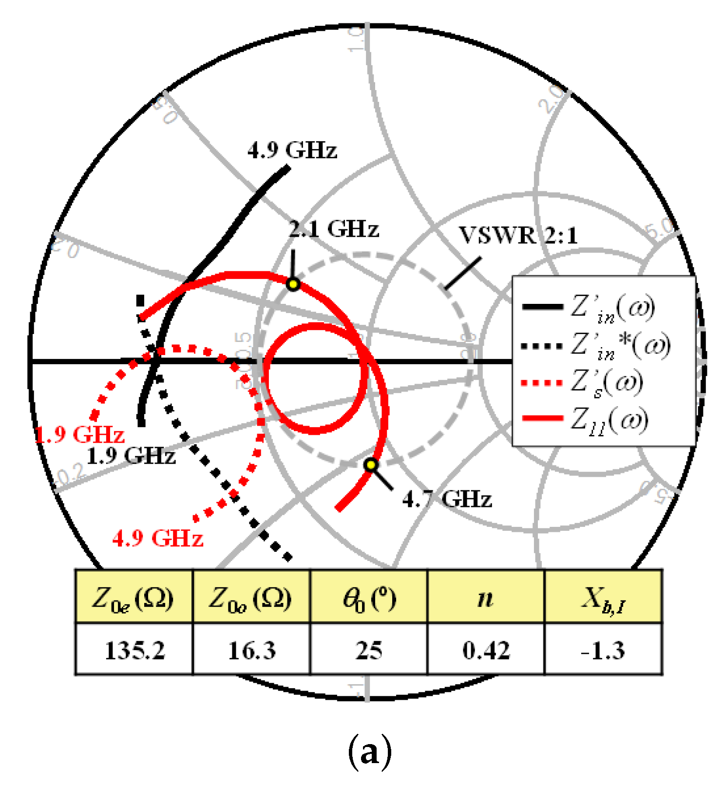
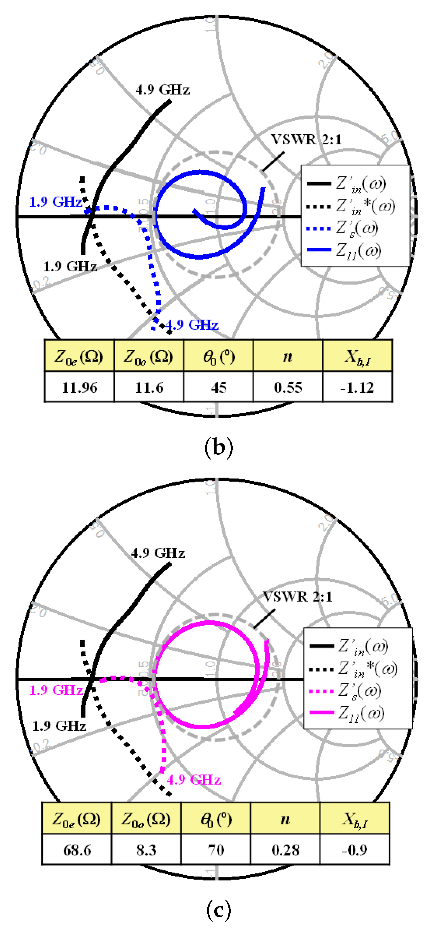
Each case is defined by a distinct set of parameters and was selected to construct input matching networks that exhibit different characteristics while maintaining an input return loss better than 10 dB across the designated frequency range. In the load matching network, the non-Foster characteristics of the CTL were tuned to maintain a constant optimal load impedance over a wide frequency band. In contrast, for the input matching network, the non-Foster behavior of the CTL must be optimized by considering the frequency-dependent input impedance Z i n of the transistor, which tends to spread over a wide frequency range. In this design, the non-Foster characteristics of the CTL were adjusted such that Z s became the complex conjugate of Z i n , ensuring conjugate matching across the operating bandwidth.
In Case 1, X 7 , I , X 8 , I , and X 9 , I exhibit non-Foster behavior, and as shown in Figure 8, their reactance values vary rapidly with frequency. As shown in Figure 9a, an input return loss better than 10 dB is achieved only within the 2.1–4.7 GHz range. In Case 2, the same elements also exhibit non-Foster behavior; however, most reactances vary more gradually with frequency. As shown in Figure 9b, Z s remains closely distributed around the complex conjugate impedance ( Z i n ) across the entire 1.9–4.9 GHz range, thereby achieving input return loss better than 10 dB throughout the band. In Case 3, all reactances show the smallest rate of change with frequency, as illustrated in Figure 9c. Nevertheless, as shown in Figure 9c, although the 10 dB input return loss condition is satisfied, Z s is less aligned with Z i n compared with Case 2, resulting in a degraded broadband matching characteristic. Therefore, the non-Foster characteristics of the CTL must be carefully optimized to suit the impedance and frequency response requirements of the corresponding matching network.

3. Implementation and Measurement Results

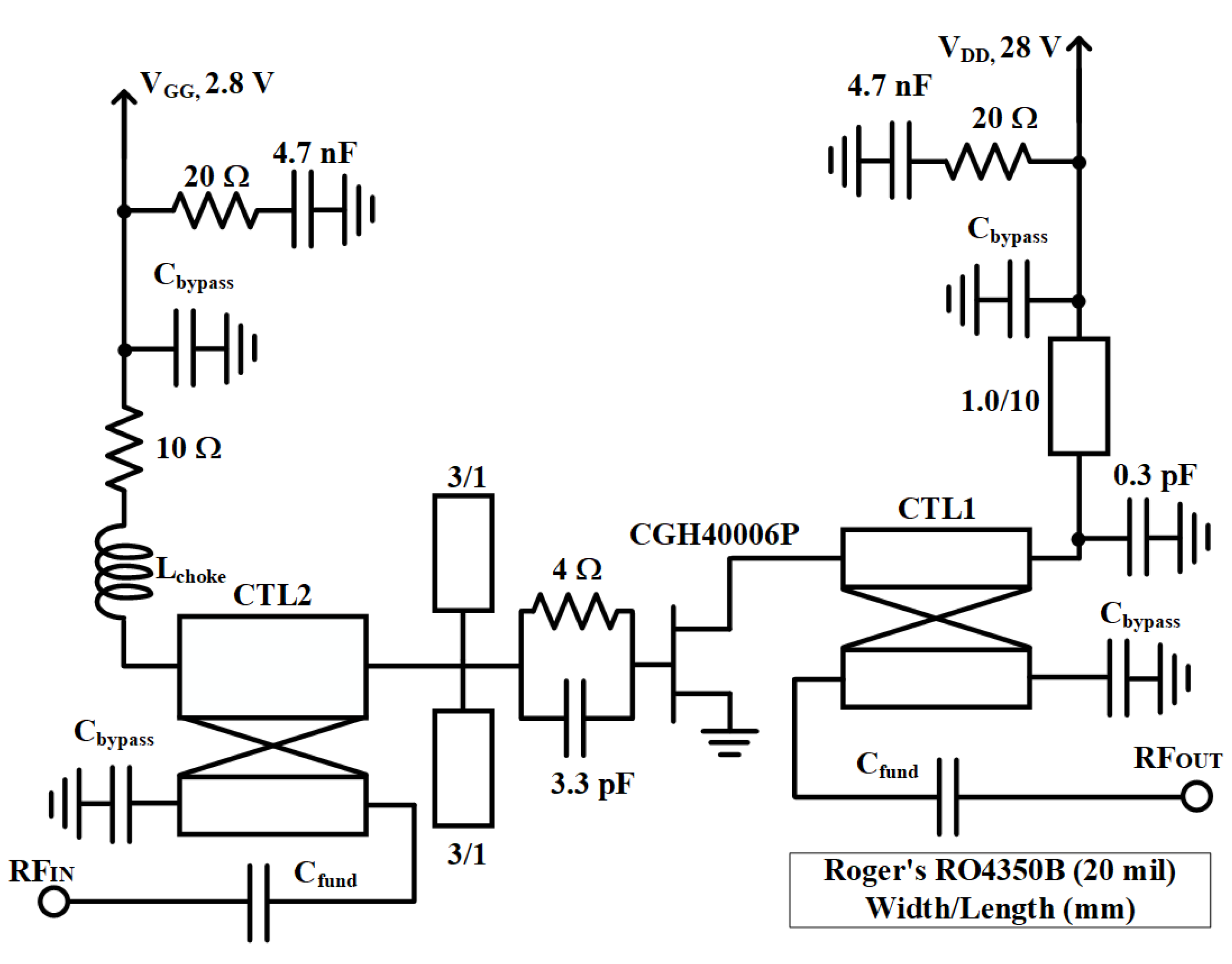
The broadband PA was designed using Cree’s CGH40006P GaN HEMT based on the proposed CTL-based impedance matching networks. Figure 10 presents the overall circuit schematic of the designed PA. The load matching network consists of a symmetric CTL with one port shorted to ground and a 0.3-pF shunt capacitor. The input matching network comprises an asymmetric CTL with one port shorted to ground, an open-circuited shunt stub, and a parallel RC network consisting of a 4- Ω resistor and a 3.3-pF capacitor for stability enhancement.
Figure 11 presents the three-dimensional structure of the input and output networks designed on a two-layer printed-circuit board (PCB). A Rogers RO4350B two-layer PCB with a thickness of 20 mil (0.508 mm) and a relative permittivity of 3.66 was employed to realize the CTL featuring electromagnetic coupling between two transmission lines. A three-dimensional electromagnetic (EM) simulation was conducted to precisely extract the characteristics of the CTL. Due to the structural characteristics of the two-layer PCB, Port 1 must be extended from the bottom layer to the top layer through a via hole, as shown in the figure.
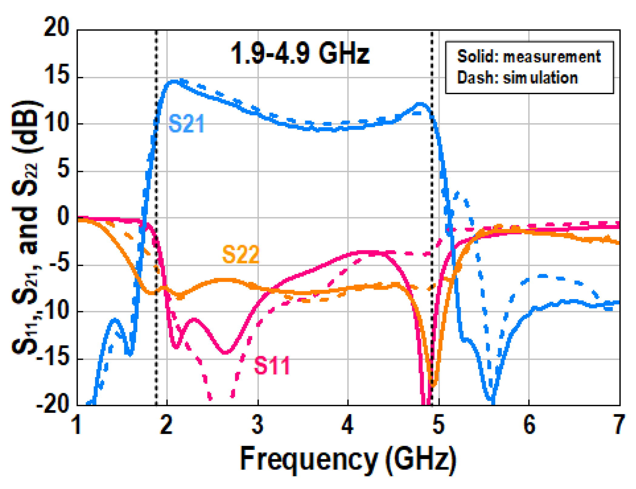
Figure 12 presents photographs of the fabricated broadband PA, including its top view, bottom view, and heat sink. The overall size of the implemented PA is 40 × 35 mm2. The PA was biased in Class-AB operation with a quiescent current of 30 mA, and the drain voltage was set to 28 V. Figure 13 presents both the simulated and measured small-signal S-parameters. The measurement results exhibit a small-signal gain higher than 10 dB within the 1.9–4.9 GHz frequency range, showing excellent agreement with the simulation over the entire band.
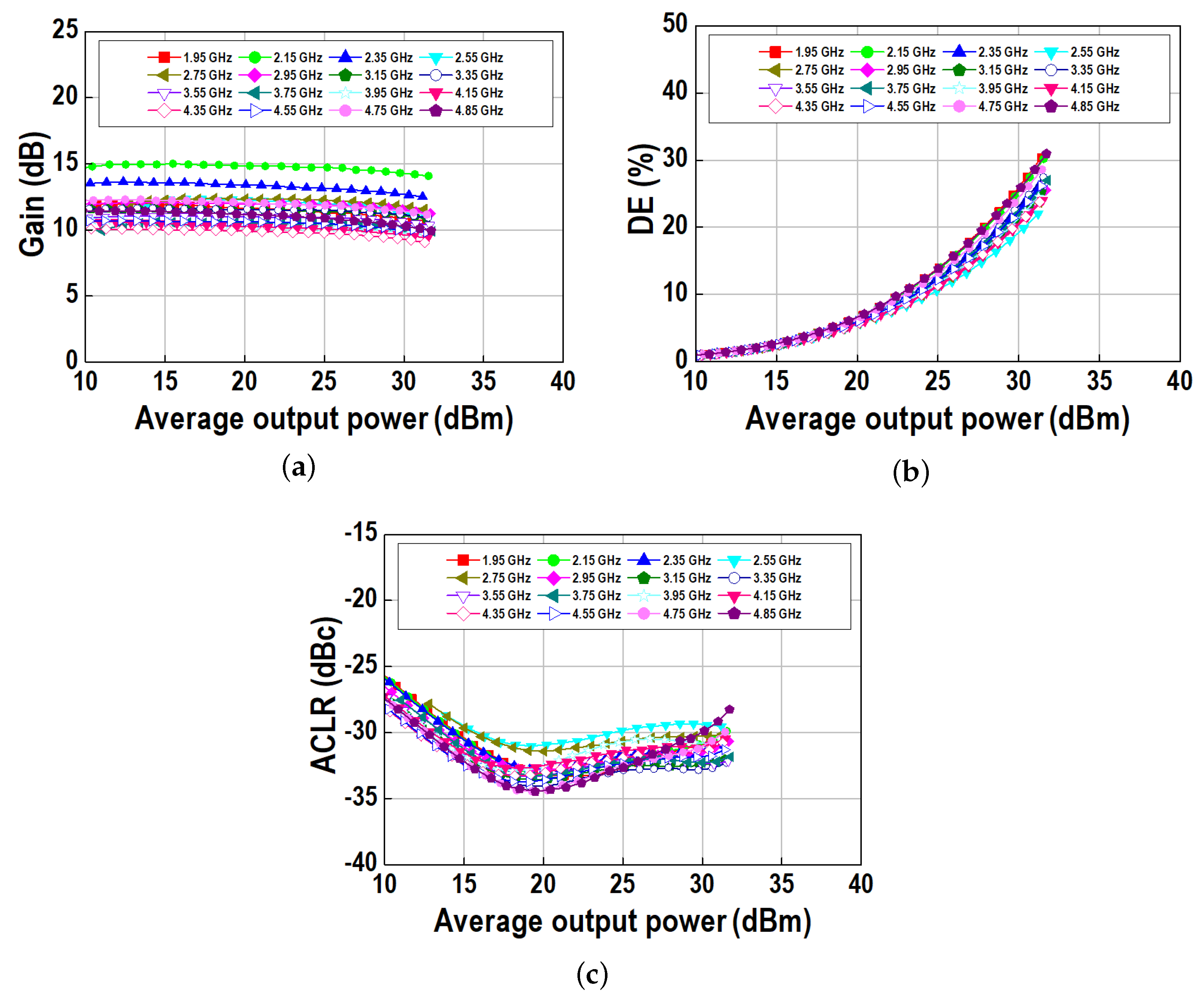
Figure 14 presents the simulated and measured results of power gain and drain efficiency (DE) under CW excitation across the 1.9–4.9 GHz frequency band. The measured results show saturated output power ranging from 38.5 to 39.5 dBm, with DE between 47.5% and 60% and a power gain of 10–14.8 dB. As shown in Figure 15, the measurement results exhibited high efficiency across the entire frequency band. Figure 16 presents the measured results obtained using a 5G NR–modulated signal with a peak-to-average power ratio (PAPR) of 7.8 dB and a signal bandwidth of 100 MHz. Figure 16 shows the measured power gain, DE, and adjacent channel leakage power ratio (ACLR) versus output power. At an average output power of 30 dBm, the proposed PA exhibited a DE of 20–27.5% and ACLR levels ranging from −28 dBc to −33 dBc. The measurement results of this work are summarized in Table 1. Compared with previous works, the proposed design achieves a wide operating bandwidth with a compact matching structure and a reduced circuit area.

4. Conclusions

In this study, a compact matching network employing a CTL was proposed for broadband power amplifier design. The proposed structure, composed of a CTL with an electrical length shorter than λ /4 and a single shunt component, demonstrated excellent broadband frequency characteristics at both the input and output networks of the transistor. Through equivalent circuit analysis, the frequency-dependent reactance variation of the non-Foster element was identified, and the matching bandwidth was extended by independently optimizing the load and input matching networks according to their respective design requirements. The proposed network was implemented in a GaN HEMT-based power amplifier designed to maintain required performances over the 1.9–4.9 GHz frequency range, covering both LTE and sub-6 GHz 5G bands. The CTL was fabricated on a two-layer PCB, and the shunt element was realized using an SMD component, resulting in a compact amplifier with a total size of 40 × 35 mm2. Under CW excitation, the fabricated PA achieved a power gain of 10–14.8 dB and DE of 47.5–60% with a saturated output power of 7.1–9.3 W across the entire frequency band. When driven by a 5G NR signal with a 100 MHz bandwidth and a PAPR of 7.8 dB, the amplifier exhibited DE of 20–27.5% and ACLR levels better than −30 dBc at an average output power of 30 dBm. These results verify that the proposed CTL-based matching network effectively achieves both wideband impedance matching and high efficiency with a compact circuit configuration, making it a promising approach for broadband and multiband RF power amplifier applications.

Author Contributions

Conceptualization, H.J.; methodology, H.J.; software, H.J. and G.M.; validation, H.J., S.B. (Sooncheol Bae) and Y.Y.; formal analysis, H.J., K.B. and M.A.; investigation, H.J., S.B. (Soohyun Bin) and Y.J.; resources, K.C.H.; data curation, K.-Y.L.; writing–original draft preparation, H.J.; writing–review and editing, K.C.H., K.-Y.L. and Y.Y.; visualization, H.J. and S.K.; supervision, Y.Y.; project administration, Y.Y.; funding acquisition, Y.Y. All authors have read and agreed to the published version of the manuscript.

Funding

This work was supported by the Technological Innovation R&D Program (SCALEUP TIPS, Tech Investor Program for Scaleup) (RS-2024-00508510) funded by the Ministry of SMEs and Startups (MSS, Republic of Korea).

Data Availability Statement

Data are contained within the article.

Conflicts of Interest

Authors Hyeongjin Jeon, Kyungdong Bae and Youngoo Yang were employed by the company para-PA Inc. The remaining authors declare that the research was conducted in the absence of any commercial or financial relationships that could be construed as a potential conflict of interest.

References

  1. Shi, W.; He, S.; Li, Q.; Qi, T.; Liu, Q. Design of broadband power amplifiers based on resistive–reactive series of continuous modes. IEEE Microw. Wirel. Compon. Lett. 2016, 26, 519–521. [Google Scholar] [CrossRef]
  2. Yang, T.; Zhou, Y.; Hong, J. A new distributed parameter broadband matching method for power amplifier via real frequency technique. IEEE Trans. Microw. Theory Tech. 2015, 63, 4258–4270. [Google Scholar]
  3. Feng, W.; Wu, W.; Zhou, X.Y.; Che, W.; Shi, Y. Broadband high-efficiency quasi-class-J power amplifier based on nonlinear output capacitance effect. IEEE Trans. Circuits Syst. II Express Briefs 2022, 69, 2091–2094. [Google Scholar] [CrossRef]
  4. Kilinc, S.; Yarman, B.S.; Ozoguz, S. Broadband power amplifier design via fictitious matching. IEEE Trans. Circuits Syst. II Express Briefs 2022, 69, 4844–4847. [Google Scholar] [CrossRef]
  5. Wang, H.; Nan, J.; Cong, M.; Ren, J. A broadband power amplifier with multifrequency impedance matching. IEEE Microw. Wirel. Compon. Lett. 2022, 32, 1339–1342. [Google Scholar] [CrossRef]
  6. Kim, Y.; Lee, D.; Kwon, S.; Kim, D.; Woo, Y.; Lee, K.-Y. Design of a compact GaN power amplifier with high efficiency and beyond-decade bandwidth. IEEE Trans. Microw. Theory Tech. 2022, 70, 1–12. [Google Scholar]
  7. Chen, Y.; Choi, W.; Shin, J.; Jeon, H.; Bae, S.; Bae, K.; Song, J.; Ju, Y.; Oh, H.; Kang, H.; et al. Comprehensive analysis of coupled transmission lines for broadband high-efficiency Doherty power amplifiers. IEEE Trans. Microw. Theory Tech. 2025; Early Access. [Google Scholar]
  8. Ju, Y.; Chen, Y.; Bae, S.; Jeon, H.; Bin, S.; Bae, K.; Lee, Y.; Woo, Y.; Lee, K.-Y.; Hwang, K.C.; et al. Load network for broadband Doherty power amplifiers using non-Foster characteristics of a coupled transmission line. IEEE Trans. Microw. Theory Tech. 2025; Early Access. [Google Scholar]
  9. Park, M.-J.; Lee, B. A symmetric coupled line equivalent circuit model for asymmetric coupled lines. Int. J. RF Microw. Comput.-Aided Eng. 2016, 26, 277–282. [Google Scholar] [CrossRef]
  10. Belchior, C.; Nunes, L.C.; Cabral, P.M.; Pedro, J.C. Automatic methodology for wideband power amplifier design. IEEE Microw. Wirel. Compon. Lett. 2021, 31, 989–992. [Google Scholar] [CrossRef]
  11. Eskandari, S.; Zhao, Y.; Helaoui, M.; Ghannouchi, F.M.; Kouki, A.B. Continuous-mode inverse class-GF power amplifier with second-harmonic impedance optimization at device input. IEEE Trans. Microw. Theory Tech. 2021, 69, 2506–2515. [Google Scholar] [CrossRef]
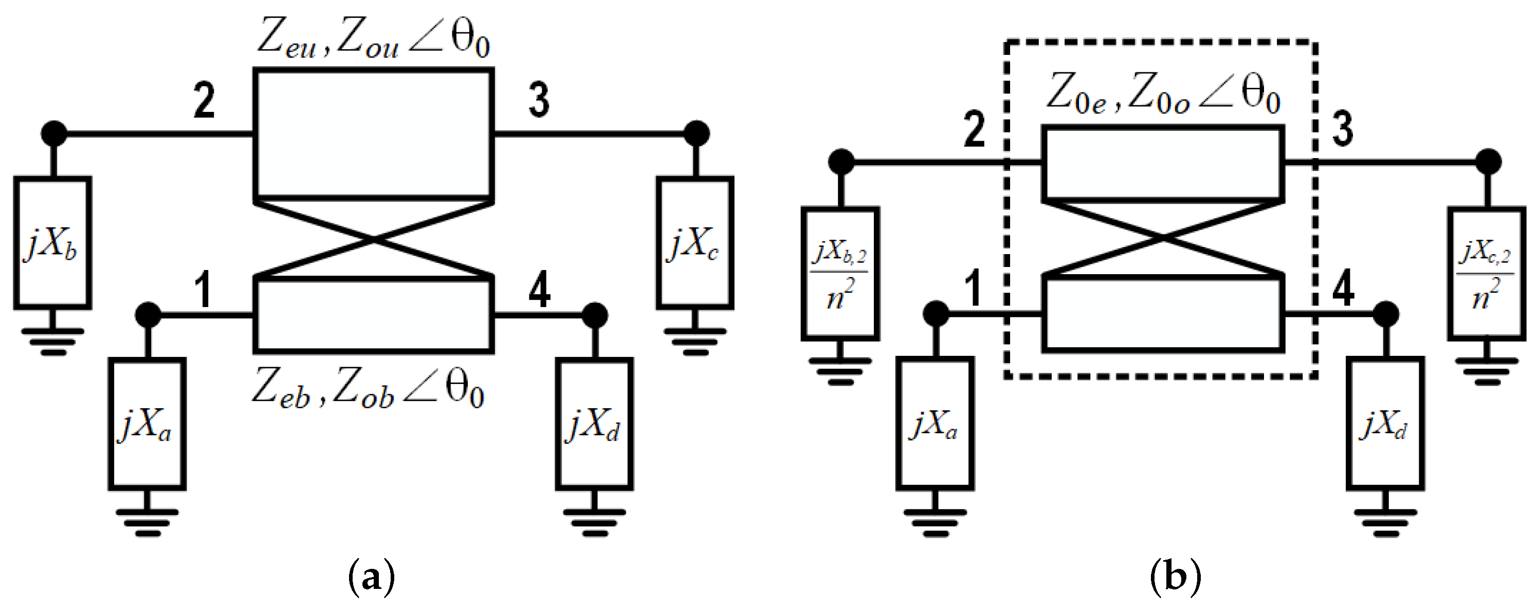
Figure 1. Asymmetric to symmetric transformation of a CTL: (a) an asymmetric CTL and (b) a symmetric CTL.
Electronics 14 04413 g001
Figure 2. Equivalent circuit of the CTL with Port 4 shorted to ground.
Electronics 14 04413 g002
Figure 3. Equivalent circuit diagram of the PA using the proposed matching networks based on CTL.
Electronics 14 04413 g003
Figure 4. Simulated contours for output power and PAE: (a) 1.9 GHz, (b) 3.4 GHz, and (c) 4.9 GHz.
Electronics 14 04413 g004
Figure 5. Calculated reactance values of the components in the equivalent circuit of the CTL for the load matching network according to the normalized frequency: (a) X 5 , L , (b) X 6 , L , (c) X 7 , L , (d) X 8 , L , (e) X 9 , L , (f) X 10 , L .
Electronics 14 04413 g005
Figure 6. Simulated impedances for the frequency range from 1.9 to 4.9 GHz for (a) Case I, (b) Case I, and (c) Case III.
Electronics 14 04413 g006
Figure 7. Simulated insertion loss of the CTL-based load network from 1.9 to 4.9 GHz.
Electronics 14 04413 g007
Figure 8. Calculated reactance values of the components in the equivalent circuit of the CTL for the input matching network according to the normalized frequency: (a) X 5 , I , (b) X 6 , I , (c) X 7 , I , (d) X 8 , I , (e) X 9 , I , (f) X 10 , I .
Electronics 14 04413 g008
Figure 9. Simulated impedances for the frequency range from 1.9 to 4.9 GHz for (a) Case IV, (b) Case V, and (c) Case VI.
Electronics 14 04413 g009aElectronics 14 04413 g009b
Figure 10. Overall schematic of the designed PA.
Electronics 14 04413 g010
Figure 11. Three-dimensional view of the matching networks including CTLs on a two-layer PCB: (a) the load matching network (CTL1) and (b) the input matching network (CTL2).
Electronics 14 04413 g011
Figure 12. Photographs of the implemented PA: (a) top view, (b) bottom view, and (c) heat sink.
Electronics 14 04413 g012
Figure 13. Simulated and measured S-parameters of the PA.
Electronics 14 04413 g013
Figure 14. Simulated and measured power gain and DE using the CW signal for the frequency band of 1.9–4.9 GHz: (a) simulated gain, (b) simulated DE, (c) measured power gain, and (d) measured DE.
Electronics 14 04413 g014
Figure 15. Simulated and measured peak output power and DE at peak power across the overall frequency band.
Electronics 14 04413 g015
Figure 16. Measured performances using a 5G NR signal with a bandwidth of 100 MHz and a PAPR of 7.86 dB: (a) gain, (b) DE, and (c) ACLR.
Electronics 14 04413 g016
Table 1. Performance summary and comparison to the previously reported broadband PAs.
Ref.Freq.FBW P sat DEGainACLR P avg DE (@ P avg )Topology
(GHz)(%)(W)(%)(dB)(dBc)(dBm)(%)
[3]3.5–5.544.49.3–13.256–708.6–10.2–2734.533Quasi-Class-J
[5]0.5–2.3128.612.7–17.543.6–55.49.8–12.7–31.634.321–26Multi-Freq. Matching
[10]1.8–2.636.022–2863–7016–17SRFT
[11]3.05–3.8523.09.8–13.869–7411–12.4–2640.035–40 *Class-GF
This work1.9–4.988.27.1–9.347.5–6010–14.8–303020–27.5CTL
* Graphically estimated.
Disclaimer/Publisher’s Note: The statements, opinions and data contained in all publications are solely those of the individual author(s) and contributor(s) and not of MDPI and/or the editor(s). MDPI and/or the editor(s) disclaim responsibility for any injury to people or property resulting from any ideas, methods, instructions or products referred to in the content.