1. Introduction
Photovoltaic (PV) systems are playing an increasingly vital role in global efforts to transition toward sustainable and clean energy solutions. As the costs of PV panels and energy storage technologies continue to decline, their deployment is rapidly expanding beyond conventional stationary applications [
1,
2]. A growing area of interest is the operation of PV systems under variable environmental conditions, where solar irradiance and loading scenarios change significantly over time due to motion, partial shading, or weather-related factors [
3,
4].
This shift has spurred a wave of research focused on improving the energy conversion efficiency and responsiveness of power electronic interfaces between PV sources and electrical loads. In such systems, the ability to adapt to fluctuations in the PV operating point becomes essential [
5]. In these contexts, the dynamic performance of DC–DC converters is critical to ensure reliable power regulation and maximum energy extraction [
6,
7].
While PV power conversion has been widely studied in the context of static installations, relatively few studies have addressed converter behavior under variable input conditions [
8]. Most existing literature primarily emphasizes steady-state performance and overlooks the transient characteristics that are crucial in PV-interfaced converters [
9]. This paper addresses this gap by focusing on the small-signal modeling and dynamic analysis of non-isolated DC–DC converters, incorporating PV panel characteristics and analyzing system behavior across different converter topologies.
Understanding the dynamic behavior of power converters is essential for optimizing their performance in photovoltaic systems where input operating conditions can vary significantly [
10,
11]. In such scenarios, accurate converter response is critical to ensure efficient energy extraction. Small-signal modeling plays a central role in this context, as it enables linearization of the converter’s nonlinear dynamics around a steady-state operating point. This allows for effective analysis of system stability and frequency response, offering a detailed view into the converter’s dynamic characteristics.
By employing small-signal analysis, we can precisely assess the speed, stability, and robustness of the converter’s control loops under varying operating conditions. This is particularly important for PV systems where shifts in the operating point directly influence converter dynamics. Consequently, small-signal models serve as a fundamental design tool for developing power converters that can reliably maintain optimal operation across a wide operating range.
In the existing literature on DC–DC converter modeling, the majority of research emphasizes the transfer function between the output voltage and the control variable, typically the duty cycle [
12,
13,
14,
15]. While this approach is suitable for conventional power electronic systems prioritizing output regulation, it is less appropriate for PV applications where the converter interfaces directly with the solar panel. In these systems, analyzing the transfer function from duty cycle to input voltage (supplied by the PV panel) is more relevant, as it provides a better understanding of how the converter dynamically adapts to changes in input power. Despite its importance, this input-side perspective has received limited attention, leaving a critical gap in the modeling of PV-interfaced converters. Addressing this gap is essential for developing accurate control strategies that enhance energy harvesting in practical photovoltaic environments.
In this work, another key novelty lies in the integration of the PV panel behavior into the small-signal representation by considering a model-derived differential resistance across various operating points. This formulation provides a consistent and realistic basis for linearization, making the small-signal model more robust and reliable for dynamic analysis. It also simplifies the characterization process and ensures that the PV–converter interaction is faithfully represented over a wide operating range [
16]. Furthermore, the small-signal analysis technique adopted in this study has proven to be highly effective in capturing the coupled dynamics of the converter and PV panel, enabling accurate derivation of the duty cycle to input voltage transfer function.
An additional contribution of this paper is the implementation of a gain-scheduling strategy for the boost converter. In this approach, the proportional–integral (PI) controller gains are adapted as a function of the PV operating point by means of a lookup table. This method ensures that the closed-loop performance remains consistent across the full range of PV voltages, overcoming the limitations of conventional controllers tuned only at the maximum power point. As demonstrated in this work, gain scheduling significantly improves transient response, stability, and tracking accuracy under varying input conditions.
The main innovations of this paper are
The derivation of analytical models for the duty cycle to input voltage () transfer function;
The integration of a model-derived differential resistance, obtained from the single-diode PV model, to represent the panel behavior under different operating conditions;
A comparative analysis of the open-loop responses of different converter topologies;
The design of closed-loop controllers essential for operating the converters under different operating conditions;
The development and validation of a gain-scheduled PI controller for the boost converter, ensuring improved closed-loop performance across the full PV operating range.
In recent years, several studies have addressed the small-signal modeling of PV-fed DC–DC converters with varying objectives, converter topologies, and levels of parasitic consideration. For example, some works have emphasized the incorporation of PV source dynamics and parasitics to improve MPPT accuracy [
17,
18], while others have extended the analysis to resonant converters and quasi-Z-source inverters [
19,
20]. A concise overview of these efforts is presented in
Table 1, which highlights the diversity in modeling approaches, the range of converter topologies explored, and the treatment of parasitic components. This comparative summary underscores the fact that although notable progress has been made, most existing studies focus on either output-oriented transfer functions or simplified models, thereby leaving a gap in accurately representing the input-side dynamics of PV-converter systems under different operating conditions. Addressing this gap forms the central motivation of the present work.
2. Small-Signal Modeling Using the State-Space Averaging Method
In the literature, small-signal models of converters are typically derived considering ideal (voltage) sources, focusing solely on the converter’s dynamics. However, the novelty of our work lies in the incorporation of the photovoltaic (PV) panel Thevenin-equivalent circuit alongside the converter. In this study, we not only derive the small-signal model for the converter but also consider the interactions between the PV panel and the converter. By doing so, we account for the coupled dynamics of both the PV panel and the converter in the small-signal analysis. This integrated approach offers a more comprehensive model that better represents the real-world behavior of the system, where both the PV panel and the converter must be considered together for accurate dynamic performance evaluation. In contrast to conventional approaches, this work incorporates the PV panel behavior into the small-signal framework by employing a model-derived differential resistance evaluated at different operating points. This formulation provides a more consistent and realistic characterization across a wide range of conditions. By relying on differential resistance, the analysis is simplified and the resulting model proves to be highly effective for control system design and dynamic performance optimization. This methodological refinement forms a central novelty of our study and ensures more robust and reliable modeling of PV–converter systems.
A state-space representation describes both the internal dynamics and output behavior of a system, governed by the state equation
where
and
are the state and input vectors, and
A and
b are the system matrices. For power converters, which alternate between ON and OFF states, the system matrices are averaged as
where
D is the duty cycle, and
and
represent the system matrices in the ON and OFF states.
For small-signal analysis, perturbations around the steady-state are defined [
25]:
The steady-state condition is
The small-signal model is
Here,
represents the perturbation in duty cycle, and
represents small variations in the input vector. In this work,
, where
is the photovoltaic (PV) voltage and
is the battery voltage. Setting
in the equation, the system’s response to duty cycle perturbations alone is
This results in the transfer function:
This transfer function captures the converter’s dynamic response to duty cycle perturbations.
2.1. Single Diode Model
Photovoltaic (PV) modules are usually characterized by key parameters such as the short-circuit current (
), open-circuit voltage (
), and the maximum power point values (
), typically reported under Standard Test Conditions (STC:
, 25 °C, AM 1.5). However, real operating conditions often deviate from STC due to variations in irradiance, temperature, and spectral effects, requiring accurate mathematical models for reliable system design and performance evaluation [
26].
Among several approaches, the single-diode model is the most widely adopted thanks to its balance between simplicity and accuracy [
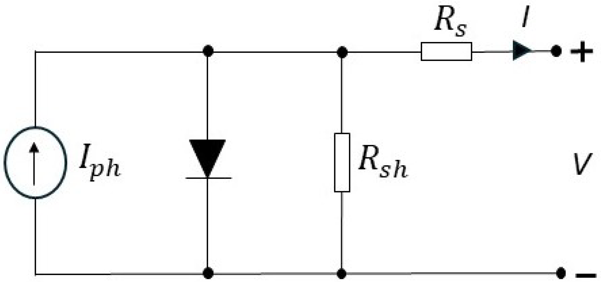
27]. The model represents the PV cell as a current source in parallel with a diode, complemented by series (
) and shunt (
) resistances to capture non-ideal effects. The photocurrent
is proportional to the incident irradiance, the diode accounts for
p–
n junction recombination,
models ohmic losses, and
represents leakage currents.
The resulting implicit current–voltage relationship of the PV cell/module is expressed as:
where
is the diode reverse saturation current,
a is the diode ideality factor, and
is the thermal voltage. This equation forms the foundation for both steady-state analysis and dynamic modeling of PV systems.
In this paper, a PV source with
,
,
,
and
has been used. These coefficients, obtained using the online Photovoltaic Modelling Tool (
https://pvmodel.umh.es/viewivdomain/1329 (accessed on 25 June 2025)) in [
28], lead to a PV panel with
,
,
and
, as shown in
Figure 1.
2.2. PV Panel Approximation
To simplify the representation of the solar panel in the proposed system, a linearized model is used. Instead of directly incorporating the nonlinear characteristics of the photovoltaic (PV) panel, the panel is replaced by its Thevenin’s equivalent circuit, consisting of a voltage source
in series with a resistance
, as shown in the derived Equation (
11). This approximation is based on the assumption that the PV panel’s behavior around its operating point can be linearized using the slope of the
ratio as
. The corresponding Thevenin’s equivalent representation of the PV panel is illustrated in
Figure 2.
The impact of duty cycle modulation on
is taken into consideration by the small-signal transfer function
.
The parameters
,
,
,
are computed. These values are then substituted into Equations (
2) and (
8) to derive the small signal transfer function
.The complete state-space matrices used for this derivation are provided in
Appendix A. To validate the derived model, a perturbation was introduced to duty cycle D and the corresponding response in the input voltage was observed. A comparison between the frequency responses obtained from the analytical transfer function and those from the simulation results are obtained.
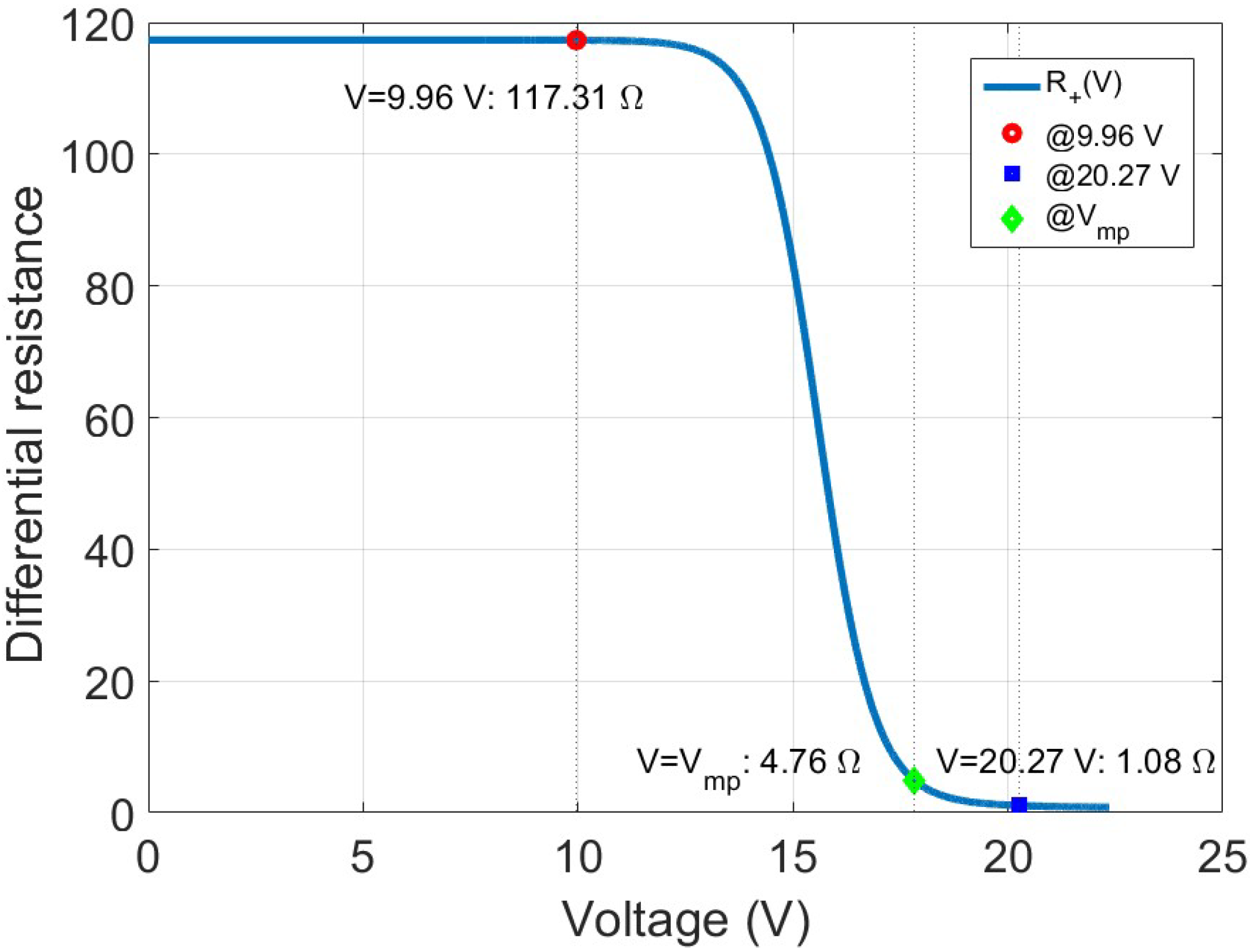
Figure 3 shows the differential resistance of the PV panel as a function of the terminal voltage
. Three important operating points are highlighted: the short-circuit region (
), the maximum power point (
), and the open-circuit region (
). As seen, the differential resistance varies strongly with the operating point. At low voltages, near short-circuit, the resistance is very high due to the steep slope of the I–V curve, while near open-circuit, the resistance becomes small. At the maximum power point, the resistance assumes an intermediate value. This behavior plays a key role in accurately representing the dynamic interaction between the PV panel and the converter in small-signal models. The differential resistance under varying irradiance and temperature conditions are further discussed in
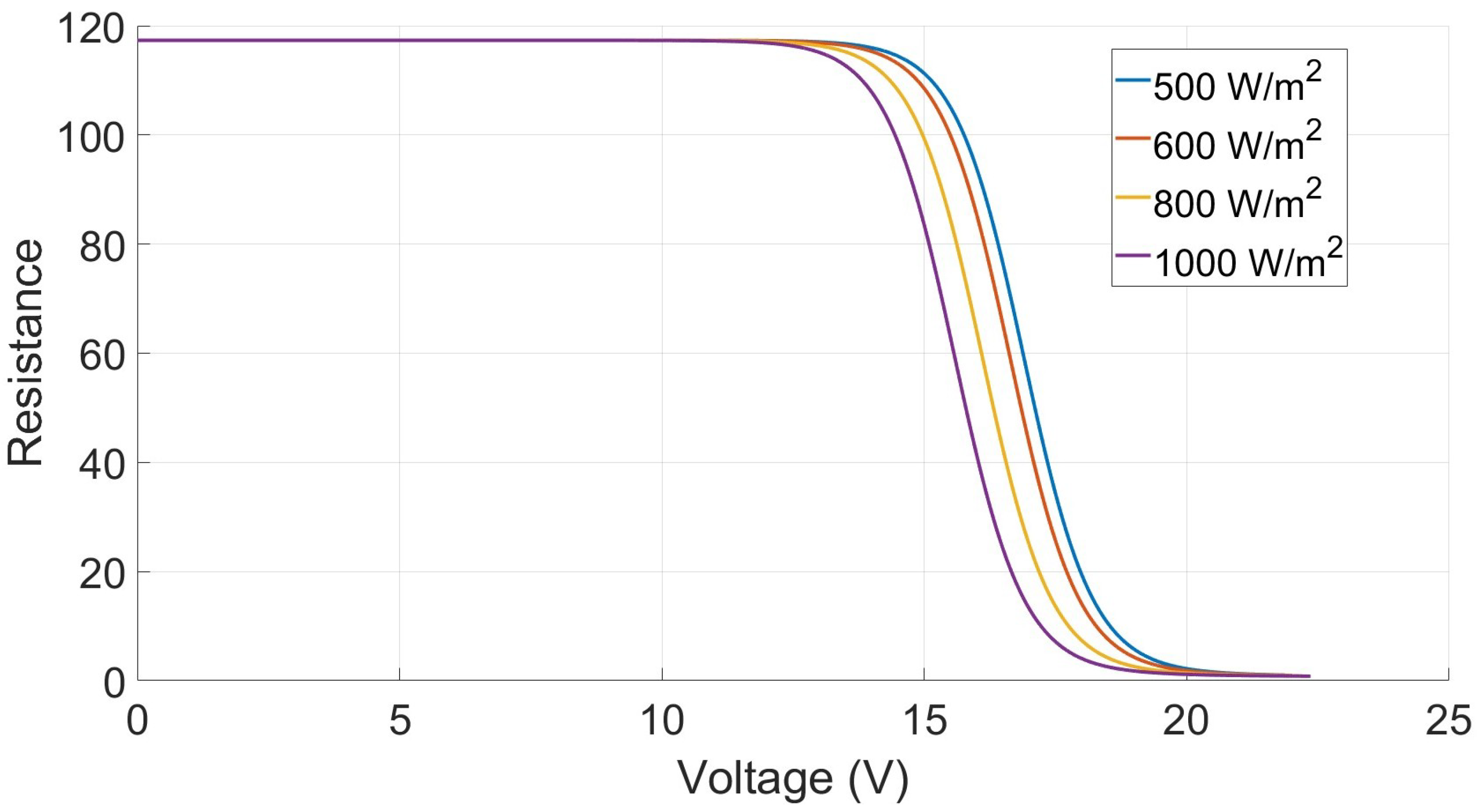
Appendix B.
The PV characteristic curve can be linearized around a chosen operating (quiescent) point denoted as
The differential resistance at this operating point is defined as
The current-voltage relationship can then be linearized using the tangent line at the following point:
This formulation is equivalent to representing the PV panel through an equivalent Norton model:
Alternatively, in Thevenin form, the PV panel can be expressed as
Thus, the slope of the I–V curve at the operating point provides the differential resistance, which directly defines the Norton or Thevenin equivalent representation of the PV source. This serves as the foundation for the small-signal modeling approach adopted in this work.
This linearization approach is applied at three distinct points on the PV curve, namely the short-circuit region, maximum power point (MPP), and open-circuit region, to improve the accuracy of the small-signal model across varying irradiance conditions.
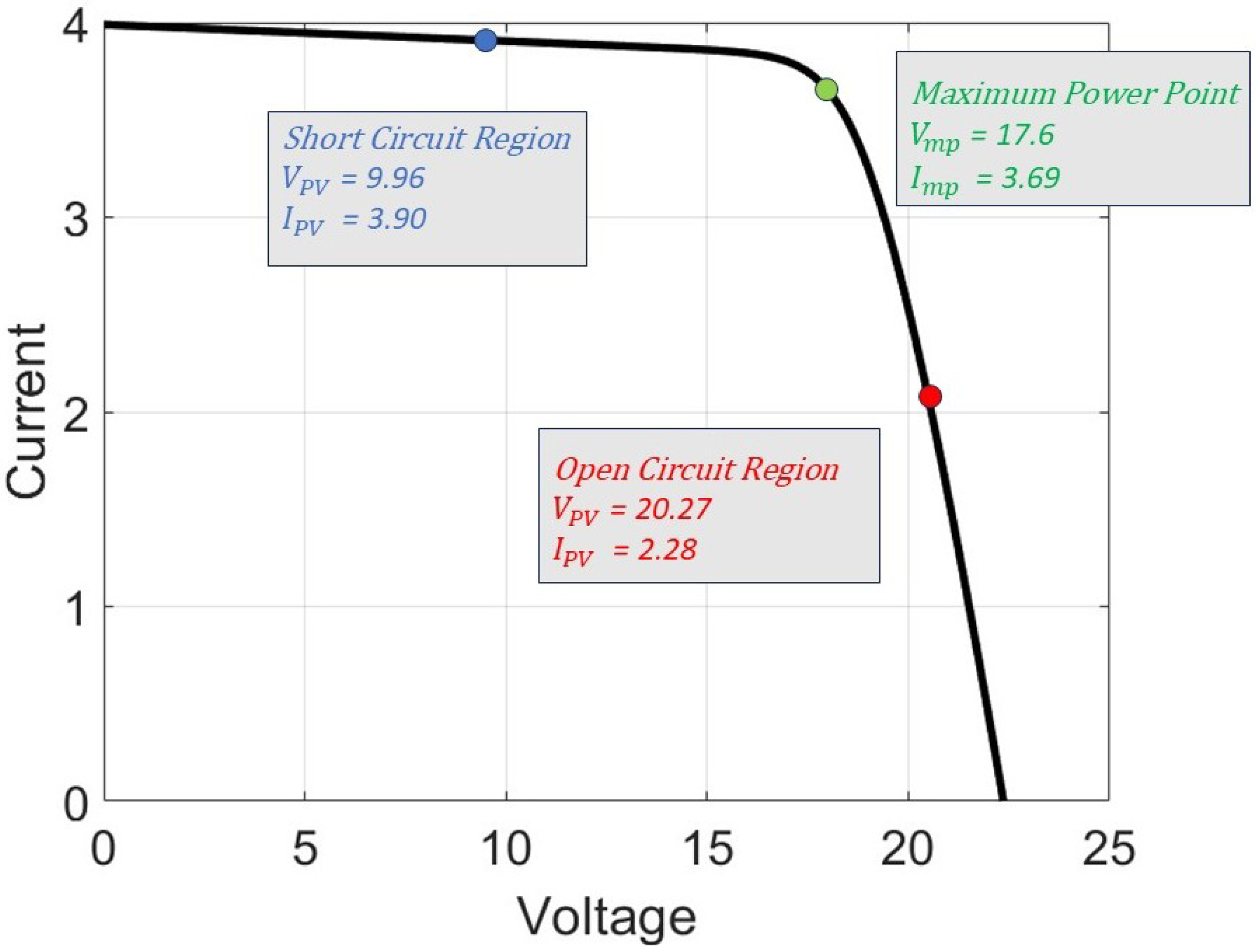
Figure 4 illustrates the current-voltage (IV) characteristic curve of the photovoltaic (PV) panel, highlighting three key operating regions that were selected for small-signal linearization and dynamic validation.
Short-Circuit Region: This point, located near the left side of the IV curve, corresponds to a high current and low voltage condition (). The dynamics in this region are dominated by high current flow and low voltage, making it essential for validating controller performance under stress conditions.
Maximum Power Point: The middle operating point () corresponds to the maximum power point (MPP), where the PV panel delivers its highest power output. This is the most critical region for MPPT control strategies, and accurate modeling here ensures efficient energy extraction.
Open-Circuit Region: Located near the right side of the IV curve, this point represents a low current and high voltage condition (). Linearization here tests the robustness of the model in scenarios with minimal load current.
These three distinct points capture the nonlinear behavior of the PV system across its full operating range. By applying small perturbations around each point and comparing the responses of the linearized and full-order models, the effectiveness and range of validity of the proposed small-signal model can be thoroughly evaluated.
2.3. Topologies Studied
This work examines four nonisolated DC–DC converter topologies, Boost, Buck–Boost, Ćuk, and SEPIC, selected to represent a broad range of dynamic and steady state behaviors relevant to photovoltaic (PV) applications. These converters were chosen not only for their structural diversity but also for their ability to reveal how different energy transfer mechanisms influence the input voltage dynamics that are central to this study’s modeling approach. Each topology exhibits distinct voltage transfer characteristics, current continuity features, and energy transfer mechanisms that directly influence the converter’s small signal response and control design.
The Boost converter is widely used in PV systems for its high voltage gain and simple structure, making it ideal for step-up operation when the PV voltage is lower than the required DC-link level. However, its discontinuous input current and relatively high output ripple can influence the input-side small-signal behavior, which is a key focus of this study. The Buck–Boost converter extends this versatility by providing both step-up and step-down capability, but it introduces voltage inversion and higher switch stress, offering an interesting contrast for evaluating input-voltage dynamics [
29].
The Ćuk and SEPIC converters, while more complex, are characterized by continuous input current and improved voltage regulation, features that make them suitable for PV systems where stable power flow and reduced ripple are critical. The Ćuk converter achieves inverting output with low ripple at both ports, whereas the SEPIC provides a noninverting output and better performance under fluctuating irradiance or load variations. These differences are illustrated in the comparative radar chart shown in
Figure 5 [
30,
31].
In the context of this research, the comparative analysis of these four converters is not limited to their static characteristics but extends to their dynamic response when interfaced with a photovoltaic source. All converters are designed under a unified set of electrical constraints, including identical operating power, switching frequency, and component ratings, to ensure an equitable comparison. Their small signal models are derived using the same linearization framework that incorporates the PV panel’s differential resistance, allowing a consistent evaluation of input and output interactions across topologies.
This unified approach enables the investigation of how each topology’s intrinsic features which affect the duty cycle to input voltage transfer function proposed in this work. Consequently, the resulting comparison provides a physically meaningful context that links the converter selection directly to the study’s objective of developing an accurate and dynamic modeling framework for PV applications.
By relating the topological characteristics to their observed dynamic behavior, this section establishes the rationale behind selecting these converters as representative cases for subsequent modeling and control design. The comparative findings also serve as a foundation for the gain scheduling control strategy analyzed later, ensuring coherence between the topology evaluation and the overall research goals.
In this study, we have excluded isolated topologies like LLC (Load-Resonant Converter) and DAB (Dual Active Bridge) due to their increased complexity, higher cost, and the challenges they introduce in terms of control and design. These converters typically require additional components, such as transformers, which significantly increase their overall cost and complexity. Moreover, isolated topologies often have higher component count, increased weight, and are more prone to efficiency losses in low-power applications, making them less practical for cost-sensitive and low-power photovoltaic (PV) systems.
The use of isolated converters, such as LLC and DAB, is typically favored in high-power applications where galvanic isolation and improved fault tolerance are crucial, and where the higher complexity and cost are justified by system requirements. For smaller-scale or cost-sensitive PV systems, however, such topologies may not provide a significant advantage, and their integration often leads to unnecessary complexity and higher production costs.
This paper focuses on non-isolated topologies, which offer several advantages in PV applications. Non-isolated converters are simpler to design, more cost-effective, and generally smaller in size. They also offer better efficiency in low-power applications and faster dynamic responses, making them more suitable for a broader range of practical uses in residential or small-scale PV systems. These advantages enable non-isolated converters to be widely adopted in distributed generation systems, where lower complexity and cost-effectiveness are key requirements.
By excluding isolated topologies, our study provides a focused comparison of dynamic performance across more commonly used converter topologies in typical PV applications. This decision reflects the goal of analyzing converters that offer practical and viable solutions for most PV systems, especially those in cost-sensitive and low-power contexts.
3. Comparative Design of Converters for Different Operating Conditions
All converter topologies in this study are analyzed in synchronous mode of operation, where the freewheeling diode is replaced by a controlled MOSFET to reduce conduction losses and improve efficiency. Furthermore, the converters are assumed to operate in continuous conduction mode (CCM), ensuring that the inductor current does not fall to zero during the switching cycle. These assumptions provide a realistic and consistent basis for comparing the performance of different topologies under different operating conditions.
The converter parameters are designed and calculated based on a set of unified constraints to enable a consistent evaluation across various topologies at three distinct operating points on the PV curve—namely, the maximum power point (MPP), an open-circuit region point, and a short-circuit region point. This multi-point linearization strategy improves the accuracy of modeling and ensures that performance differences arise from the inherent characteristics of each topology rather than variations in design conditions, making the comparison fair and technically sound.
The key constraints considered for component selection and system analysis are listed below for each operating point:
At Maximum Power Point (MPP):
Input Voltage: V;
Input Current: A;
Input Resistance: .
At Open-Circuit Region Point:
Input Voltage: V;
Input Current: A;
Input Resistance: .
At Short-Circuit Region Point:
Input Voltage: V;
Input Current: A;
Input Resistance: .
Common Parameters:
Ripple Current in Inductor (): Maintained at 0.1 A to ensure minimal losses and stable operation.
Voltage Ripple of Input Capacitance (): Constrained to 0.1 V to minimize input fluctuations.
Switching Frequency (): Set at 50 kHz to balance efficiency and component sizing.
Parasitic Resistances: The parasitic resistances of MOSFET switches, inductors, and capacitors are each considered as 0.1 in the simulations.
These constraints serve as fundamental design parameters for the precise computation of various components in the converter system. The configuration of the photovoltaic (PV) panel utilized as the input source for the various converter topologies is detailed in
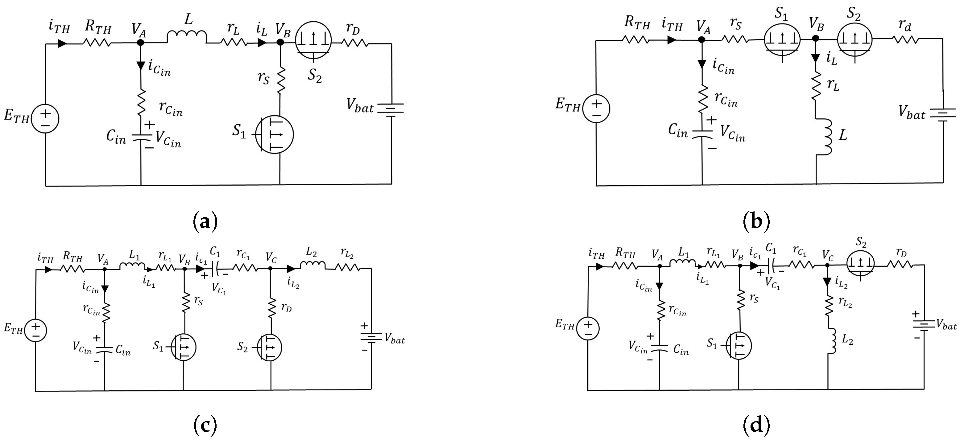
Table 2. The Thevenin equivalent circuit representations for the various DC–DC converter topologies are shown in
Figure 6.
3.1. Boost Converter
The key parameters of the boost converter, including duty cycle, inductance, and input capacitance, are calculated to ensure efficient performance and voltage stability.
The duty cycle (
D) of the boost converter is given by
The inductance (
L) required for the boost converter can be determined using
The required input capacitance (
) is calculated as
These calculations establish the fundamental design parameters for the boost converter, ensuring stable operation, reduced ripple, and efficient energy conversion.
3.2. Buck-Boost Converter
The following calculations determine the key parameters of the buck-boost converter, including the duty cycle, inductance, and input capacitance, ensuring stable and efficient operation.
The duty cycle (
D) for a buck-boost converter is given by
The required inductance (
) is calculated using
The required input capacitance (
) is determined using
These calculations provide the essential design parameters for the buck-boost converter, ensuring proper voltage regulation, reduced ripple, and stable performance.
3.3. Ćuk Converter
This section presents the key parameter calculations for the Ćuk converter, including the duty cycle, inductance, output current, and input capacitance. The design values are determined based on the given input and output specifications.
The duty cycle
D of a Ćuk converter is given by
The inductance values
and
are calculated using the standard expression:
These inductance values ensure proper energy transfer and current ripple control in the converter.
The output current
is determined using
The selection of the coupling capacitor
is based on the following expression:
The input capacitor
is selected to ensure a stable input voltage. The chosen capacitance value is
with an associated voltage ripple of
A properly selected input capacitor minimizes voltage fluctuations and enhances the overall performance of the converter.
The calculated values of the duty cycle, inductances, output current, and input capacitance ensure efficient operation of the Ćuk converter.
3.4. Sepic Converter
This section presents the design calculations for the Single-Ended Primary Inductor Converter (SEPIC), including the duty cycle, inductor sizing, output current, capacitor selection, and input voltage ripple considerations.
The duty cycle
D for the SEPIC converter is determined by
This duty cycle governs the switching operation and the component selection for the converter.
The inductance values
and
are computed using
where
is the switching frequency, and
is the inductor current ripple.
These inductance values ensure proper energy transfer and minimize current ripple in the converter.
The output current
is determined using
This output current value is crucial for analyzing the converter’s load-handling capacity.
The selection of the coupling capacitor
is based on the following expression:
Proper capacitor selection helps in maintaining voltage stability and reducing ripple effects.
The chosen input capacitance is
A well-sized input capacitor minimizes input voltage fluctuations, thereby enhancing the performance and efficiency of the SEPIC converter.
The calculated duty cycle, inductance, output current, and capacitance values ensure the efficient operation of the SEPIC converter.
The calculated duty cycle, inductance, and capacitance values for various DC–DC converter topologies operating at the Maximum Power Point are summarized in
Table 3.
The component values for each converter topology shown in
Table 4 are determined considering the operating point in the open-circuit region of the PV panel, where
V and
A. This ensures accurate modeling under high-voltage, low-current conditions.
The component parameters for each converter topology, as presented in
Table 5, are determined by considering a point in the short-circuit region of the PV panel, where
and
. This specific condition represents a low-voltage, high-current scenario, which is important for evaluating converter behavior under electrically stressed conditions.
4. Comparative Analysis
4.1. Open-Loop Analysis and Comparison
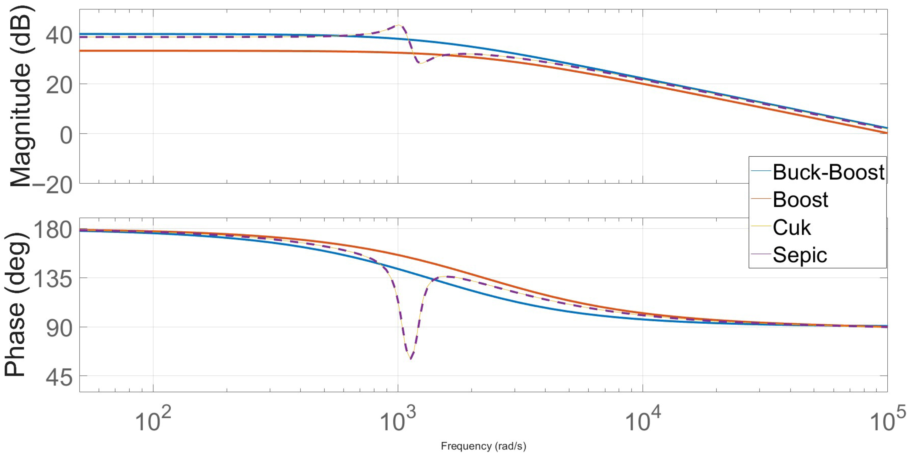
Figure 7 shows the Bode diagrams of the open-loop transfer function between the input voltage (
) and the duty cycle (
d) for commonly used DC–DC converter topologies: Boost, Buck–Boost, Ćuk, and SEPIC. These frequency-domain responses provide critical insights into the dynamic behavior and control requirements of each topology, particularly in photovoltaic (PV) applications. Notably, resonance humps appear only in the Ćuk and SEPIC converters, while the Boost and Buck-Boost converters do not exhibit these features.
The resonance humps in the Ćuk and SEPIC converters arise due to the interaction between the inductors and capacitors in their topologies, creating resonant frequencies at specific points in the frequency spectrum. These converters have more complex energy storage configurations, with the Ćuk featuring a coupled inductor and the SEPIC using a dual inductor structure, both of which are more prone to resonance effects. This results in the distinct resonance humps observed in their Bode plots.
In contrast, the Boost and Buck-Boost converters have simpler topologies with single inductors, which do not exhibit such pronounced resonant peaks. The absence of resonance in these converters is a characteristic of their design, where the frequency response is smoother due to the simpler energy transfer mechanisms.
This analysis highlights the frequency-dependent behavior of each converter and the impact of their different topologies on the dynamic performance. The resonance humps observed in the Ćuk and SEPIC converters provide insight into the effects of more complex topologies on the converter’s dynamic response.
The open-loop Bode analysis of the four converters reveals broadly similar low-frequency behavior, with all topologies exhibiting flat gain that confirms steady-state regulation. Differences emerge in the mid- to high-frequency range: the Boost converter maintains the smoothest magnitude roll-off and most gradual phase decline, indicating well-damped dynamics and a wide phase margin. The Buck–Boost converter shows a stronger high-frequency gain reduction and a somewhat faster phase roll-off, though still without pronounced resonance. By contrast, the Ćuk and SEPIC converters display clear resonance humps in magnitude accompanied by sharp phase dips near the kHz range, with SEPIC showing the most pronounced effect. These dynamic characteristics suggest that while Boost and Buck–Boost are inherently more stable in open loop, Ćuk and SEPIC require more careful compensator tuning to achieve robust closed-loop performance.
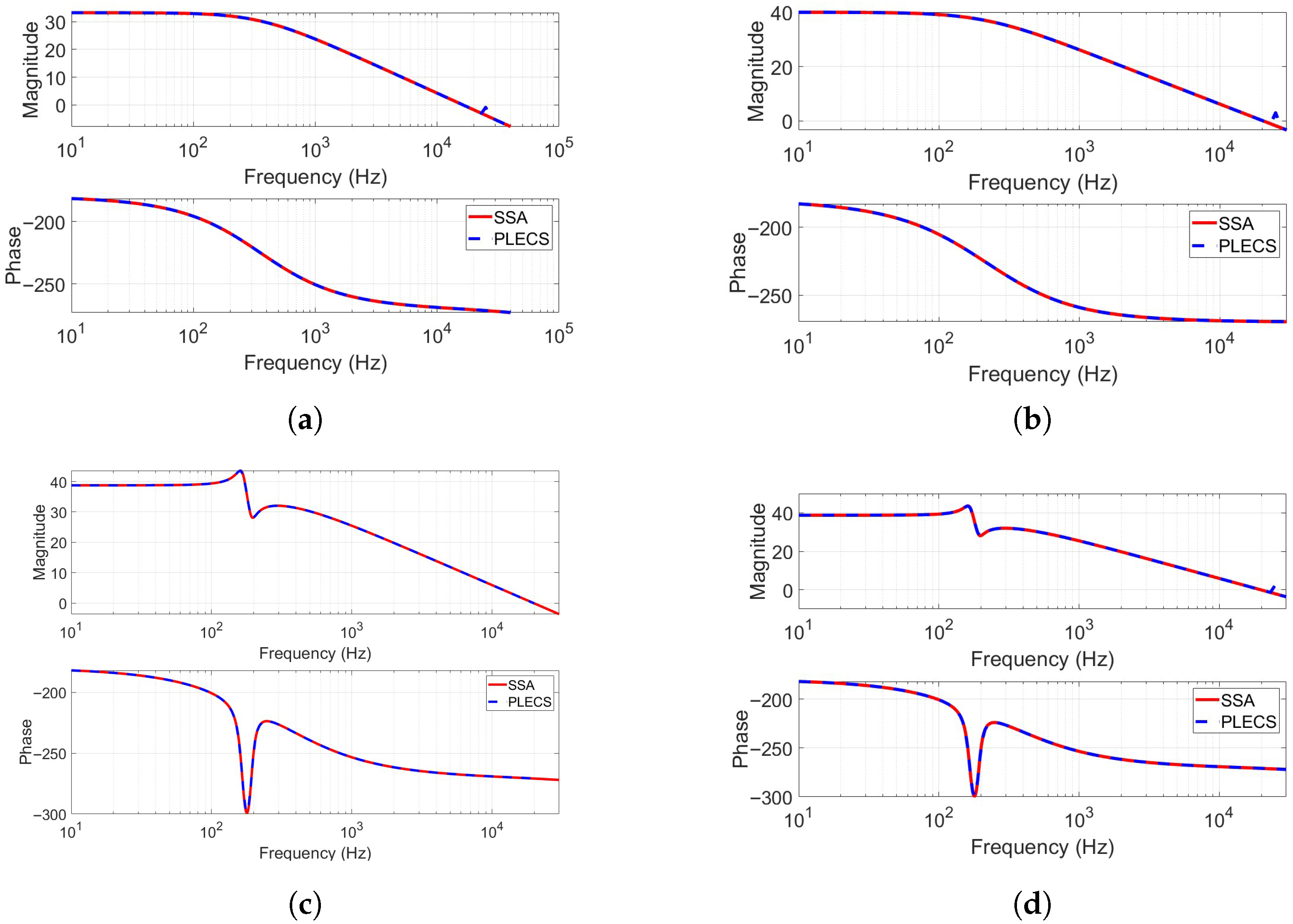
Figure 8 illustrates the frequency response comparison between the analytically derived small-signal models (SSA) and the PLECS-based simulation models for four different non-isolated DC–DC converter topologies: Boost, Buck-Boost, Ćuk, and Sepic. The close agreement between the Bode plots in terms of both magnitude and phase across a wide frequency range validates the accuracy of the proposed linearization approach. This consistency confirms that the developed small-signal models incorporating photovoltaic dynamics and using the differential resistance concept reliably capture the dynamic behavior of the converters under realistic operating conditions.
4.2. Closed-Loop Analysis
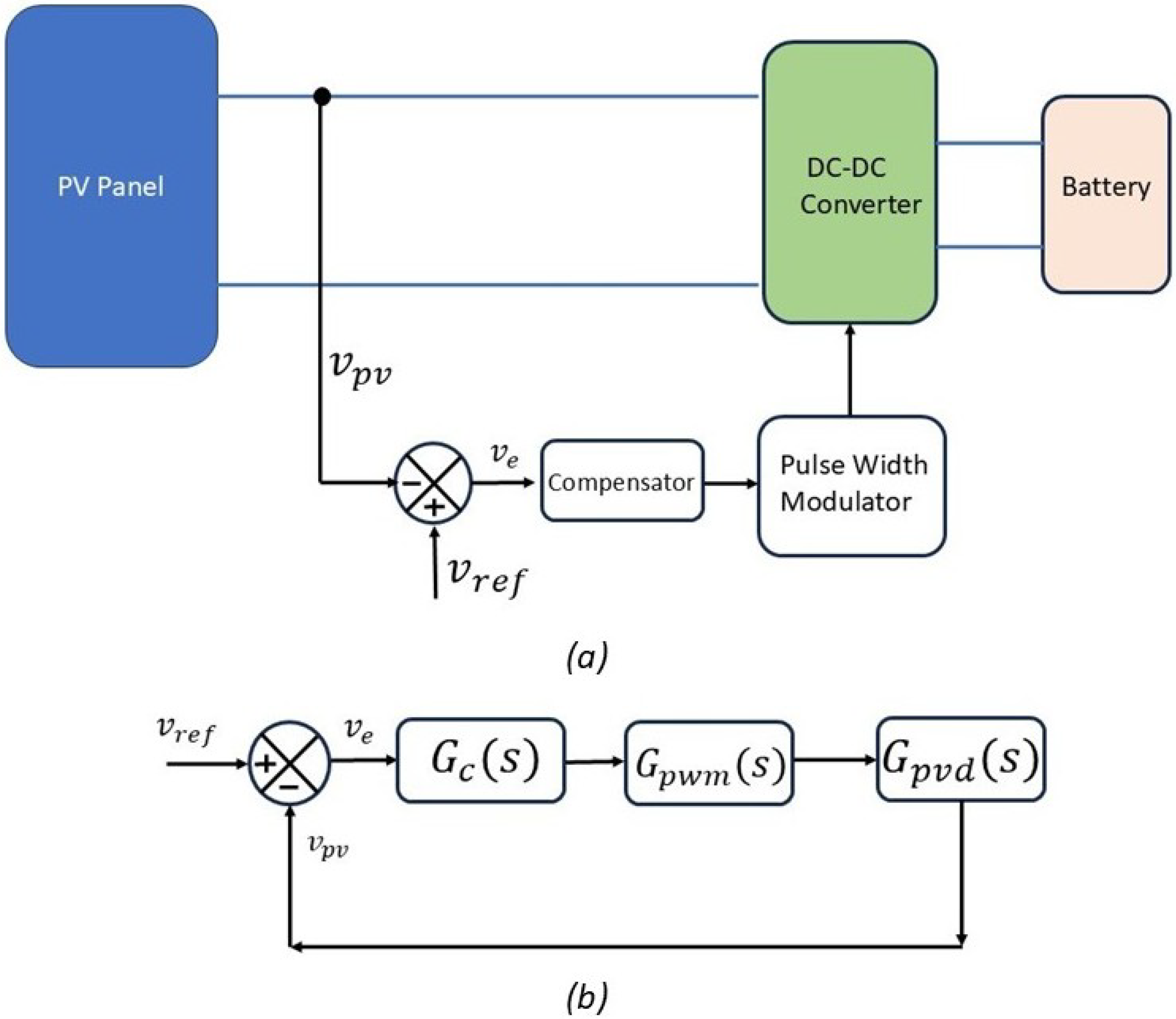
Figure 9 illustrates a control scheme for regulating the operation of a photovoltaic (PV) system connected to a DC–DC converter. In this configuration, the PV panel generates a voltage
, which serves as the primary feedback signal for the control loop.
The actual PV voltage is continuously compared with the reference using a subtractor block. The result of this comparison is the error signal , which quantifies the deviation of the operating point from the desired setpoint.In this study, the reference voltage is not fixed to the maximum power point (MPP) alone. Instead, it is varied across three distinct operating points for linearization and dynamic analysis: the MPP voltage , the PV voltage in the short-circuit region, and the PV voltage in the open-circuit region. This multi-point approach enables the evaluation of converter dynamics under different operating scenarios and improves the generalization of the small-signal model.
This error signal represents the deviation from the operating point and is used as the input to a compensator with a transfer function . The compensator is designed to ensure system stability and dynamic response.
The output of the compensator is passed to a pulse width modulator (PWM), which adjusts the duty cycle of the DC–DC converter accordingly. By modulating the converter’s switching behavior, the system dynamically aligns the PV operating point with the desired power point.
This approach enables effective regulation of the PV voltage and forms the basis of the closed-loop control mechanism that drives the pulse width modulation and DC–DC converter stages.
Notably, the compensator . is designed such that the phase margin and phase crossover frequency remain consistent across different converters.The phase margin was set at to ensure a good balance between system stability and dynamic response across all converter topologies. A phase margin in the range of – is typically considered optimal in control system design, as it provides adequate damping without making the system too sluggish. Selecting allows for consistent comparison among the converters under similar dynamic stability conditions.
The crossover frequency was selected as , where is the switching frequency. Since the switching frequency is , the corresponding crossover frequency is for all topologies. This choice maintains a sufficient separation between the control bandwidth and the switching frequency, thereby avoiding high-frequency noise amplification while ensuring a fast control response. This ensures a fair performance comparison between converters under varying operating conditions, allowing for an objective evaluation under identical control conditions.
5. Gain Scheduling
In order to ensure robust closed-loop performance of the boost converter under varying photovoltaic (PV) operating conditions, a gain-scheduling strategy was adopted. The scheduling variable was chosen as the differential resistance , which characterizes the dynamic behavior of the PV source at different points of its I–V curve.
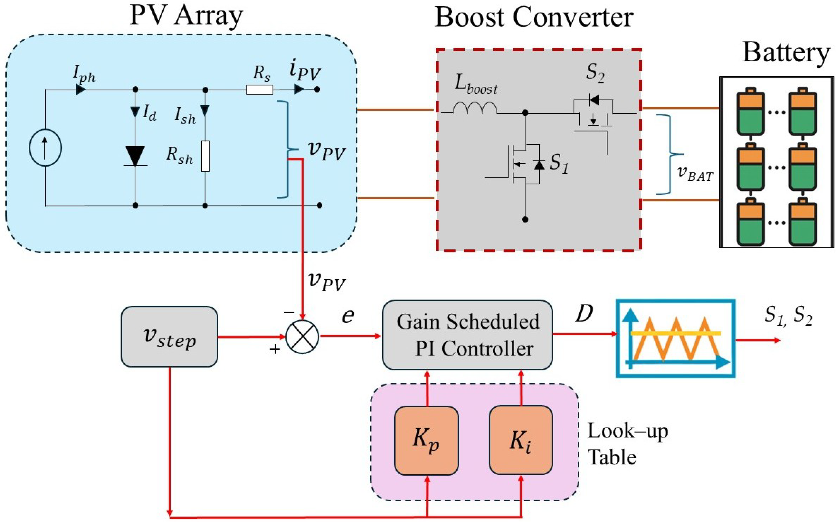
The overall control structure of the proposed gain-scheduled PI controller is illustrated in
Figure 10. The diagram shows the interaction between the PV array, Boost converter, and the controller. The PV voltage (
) is compared with a reference signal (
) to generate the error signal (
e), which is processed by the gain-scheduled PI controller. The proportional (
) and integral (
) gains are adaptively selected from a look-up table according to the PV operating point, and the resulting duty cycle (
D) drives the converter switches to regulate the PV voltage and ensure optimal power extraction.
The differential resistance of the PV source can be obtained from the one-diode model. The implicit current–voltage relation is given by
where
is the photocurrent,
is the reverse saturation current,
a is the diode ideality factor,
is the thermal voltage,
is the series resistance, and
is the shunt resistance.
The differential resistance is defined as
Since
, implicit differentiation yields
with partial derivatives
Thus, the differential resistance of the PV source can be written as
For each value of , the corresponding PV voltage was obtained by interpolation. A proportional–integral (PI) controller was then tuned for each operating point using the MATLAB pidtune function, with the design objectives of a same crossover frequency and phase margin.
For each value of , the corresponding PV voltage was obtained by interpolation. A proportional–integral (PI) controller was then tuned for each operating point using the MATLAB R2024b pidtune function, with the design objectives of a same crossover frequency and phase margin.
The gain-scheduling lookup table was generated from a parameter sweep of the PV-side differential resistance () ranging from 0.83 to 117.33 , corresponding to the full voltage range of the PV module. A total of 50 uniformly spaced sampling points were used to compute the PI controller gains (, ) using MATLAB’s pidtune function with a target crossover frequency of 5 kHz and a phase margin of 50°. Linear interpolation was adopted to estimate intermediate values, ensuring smooth variation of the controller parameters across the operating range. A nearest-neighbor fallback was implemented for undefined samples to maintain numerical continuity and stability of the gain transitions.
After computing the proportional and integral gains
at different PV operating points (for example, at various values of
), the results were stored in one-dimensional lookup tables. These tables were then used to provide the corresponding controller gains to the PI regulator, as illustrated in
Figure 11. In this configuration, the controller automatically selects appropriate
and
values depending on the instantaneous PV operating voltage. To validate the performance, a step sequence in the reference voltage
was applied. The gain-scheduled PI controller demonstrated stable operation across the full range of conditions, confirming that the scheduled gains successfully adapt the control action to different operating points.
6. Results
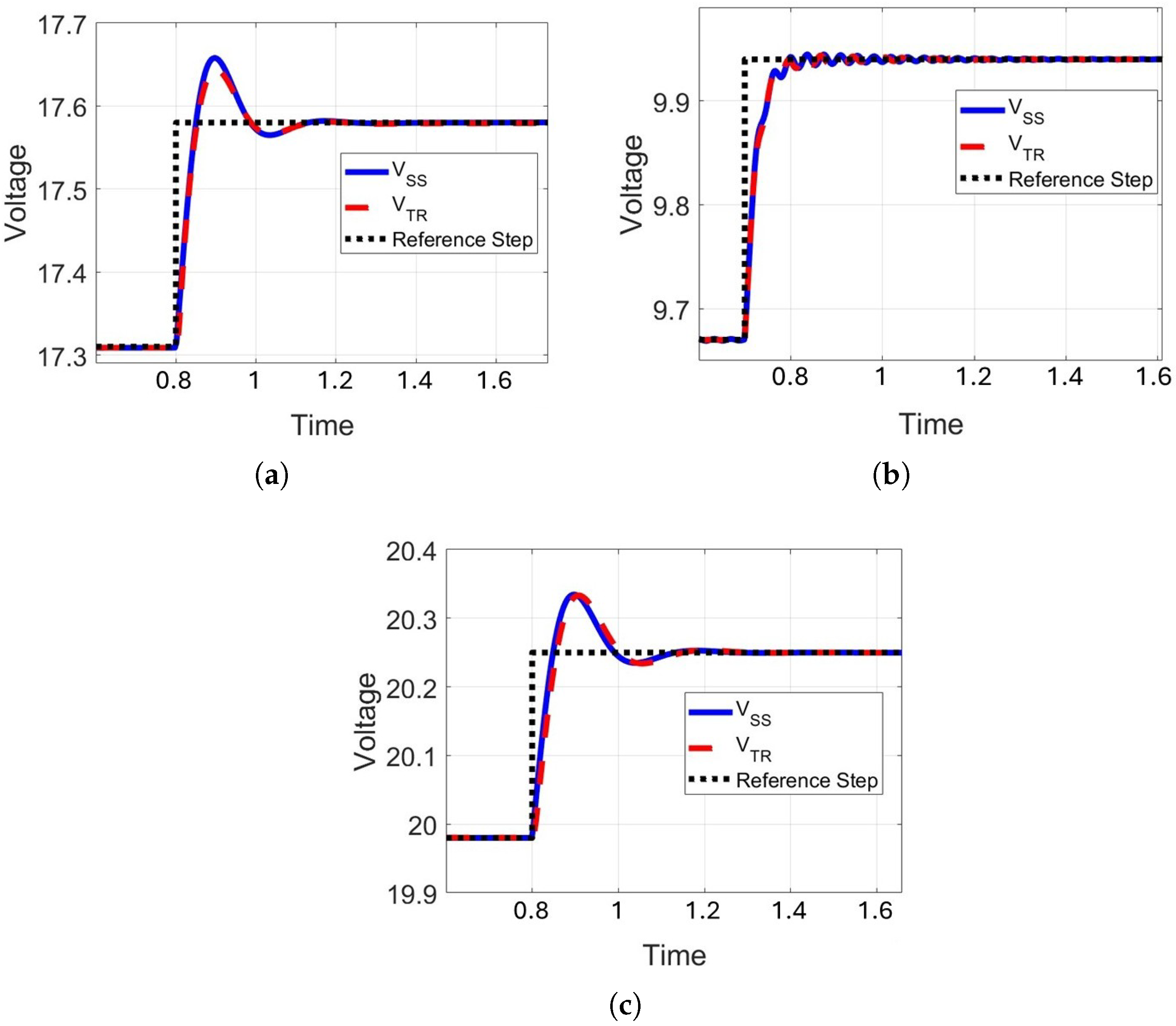
Figure 12 shows the closed-loop voltage response of the boost converter under small perturbations applied at three operating points: (a) maximum power point (MPP) region, (b) open-circuit region, and (c) short-circuit region. The applied step represents a small deviation to evaluate the system’s dynamic performance.
In each plot, the nonlinear time-domain response (red dashed line) is compared with the corresponding linearized small-signal response (blue solid line), while the black dotted line indicates the reference input step. The close superposition of the two responses across all regions highlights the consistency and predictive capability of the small-signal model.
This demonstrates that the small-signal linearization technique, although developed locally at each operating point, matches the nonlinear dynamics not only at the MPP but also under extreme conditions, validating its robustness and suitability for control design and stability analysis of the boost converter. By accurately capturing the essential dynamics, the small-signal model provides a reliable and computationally efficient tool for converter analysis without the need for full nonlinear simulations.
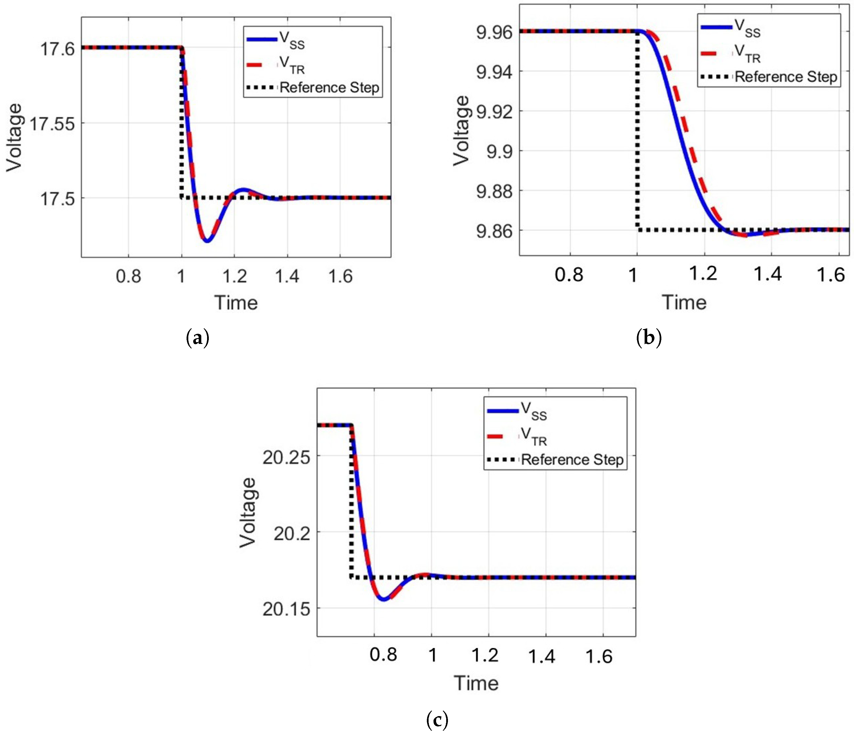
Figure 13 illustrates the small-signal linearization validation for the buck–boost converter under three operating points: (a) maximum power point (MPP), (b) short-circuit region, and (c) open-circuit region. A small perturbation is applied to excite the system dynamics.
The comparison between the nonlinear time-domain response
and the small-signal model
, with the reference step shown in black, demonstrates that the linearized model captures the converter’s behavior accurately. At the MPP (
Figure 13a), both models exhibit nearly identical responses. In the short-circuit case (
Figure 13b), the linear model reproduces the slower recovery trend of the actual dynamics. In the open-circuit condition (
Figure 13c), the linearized trajectory aligns well with the nonlinear model, despite minor deviations during the initial transient.
These results show that the small-signal linearization framework is robust across a wide range of conditions, supporting its use in controller design, sensitivity studies, and stability assessments without relying on full nonlinear simulations.
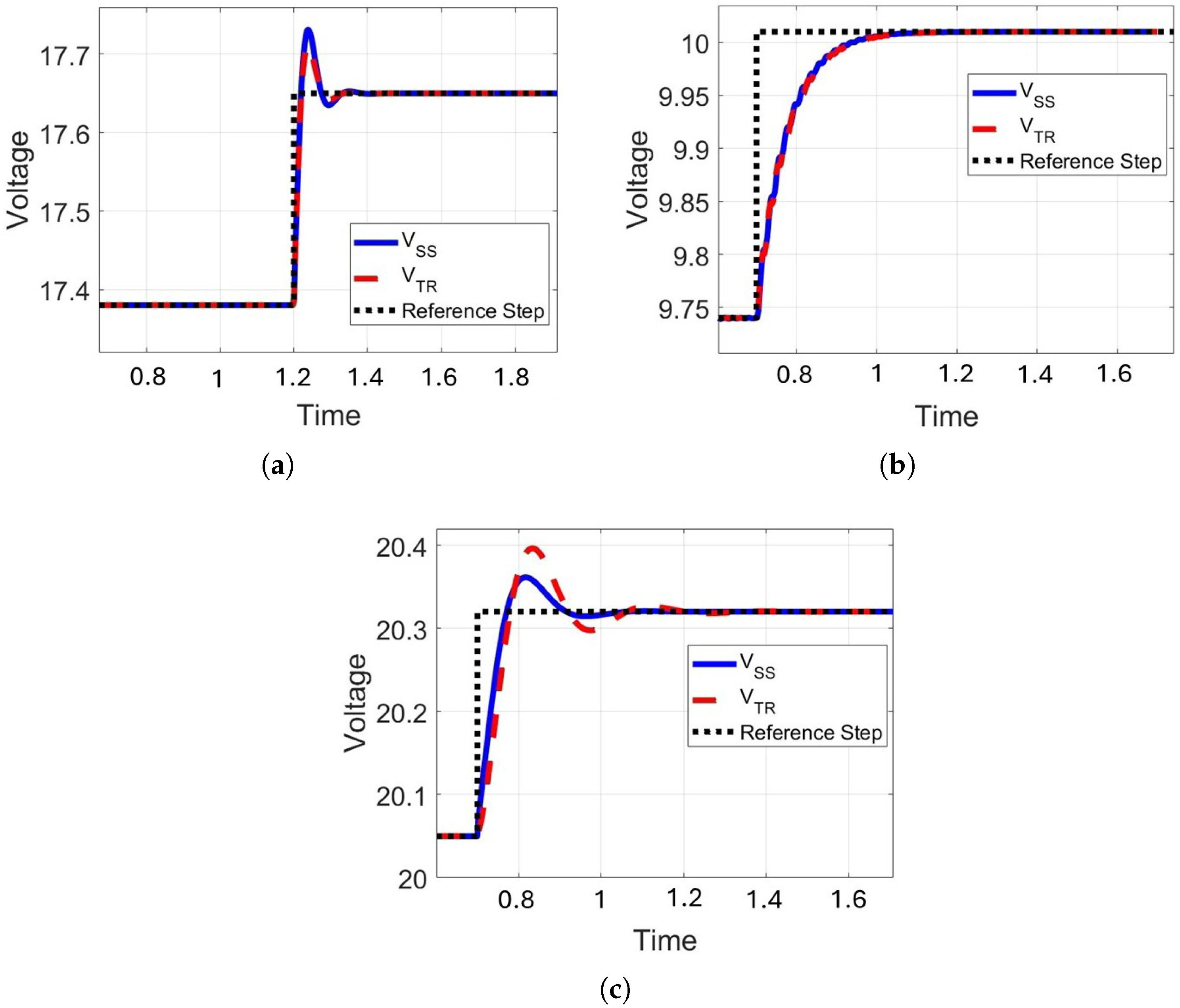
Figure 14 presents the closed-loop voltage response of the Ćuk converter with a small perturbation at three operating points: (a) maximum power point (MPP), (b) short-circuit region, and (c) open-circuit region. The reference step input is marked by the black dotted line, and the nonlinear response
is compared against the small-signal response
.
At the MPP (
Figure 14a), the two responses closely overlap, validating the linearization around the optimal operating point. In the short-circuit condition (
Figure 14b), the linearized model accurately reproduces the nonlinear dynamics. Similarly, under open-circuit operation (
Figure 14c), the models remain nearly indistinguishable.
These results highlight the robustness of the linearization method for converters with complex energy transfer characteristics, such as the Ćuk topology. The small-signal model proves to be a reliable tool for performance evaluation, sensitivity studies, and controller synthesis.
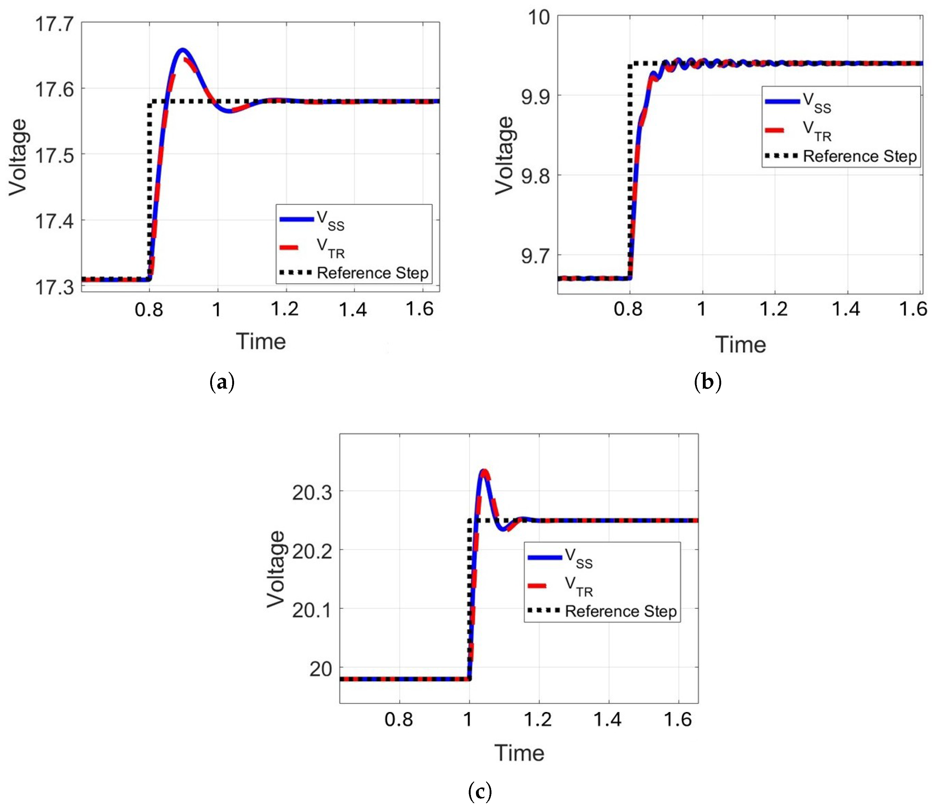
Figure 15 shows the dynamic validation of the small-signal model for the SEPIC converter under three operating points: (a) maximum power point (MPP), (b) short-circuit region, and (c) open-circuit region. The plots compare the nonlinear response
with the small-signal response
, with the reference step marked in black.
Across all conditions, the small-signal model accurately follows the nonlinear dynamics. At the MPP (
Figure 15a), the responses are nearly identical, demonstrating the linear approximation’s accuracy. In the short-circuit condition (
Figure 15b), the model captures the smooth recovery of the system. Under open-circuit operation (
Figure 15c), the linearized model aligns well with the nonlinear trajectory, reproducing both the transient overshoot and steady-state settling.
The small-signal model’s ability to represent the SEPIC converter’s dynamics in all regions confirms the robustness of the linearization method, making it a reliable framework for a variety of converter topologies and operating conditions.
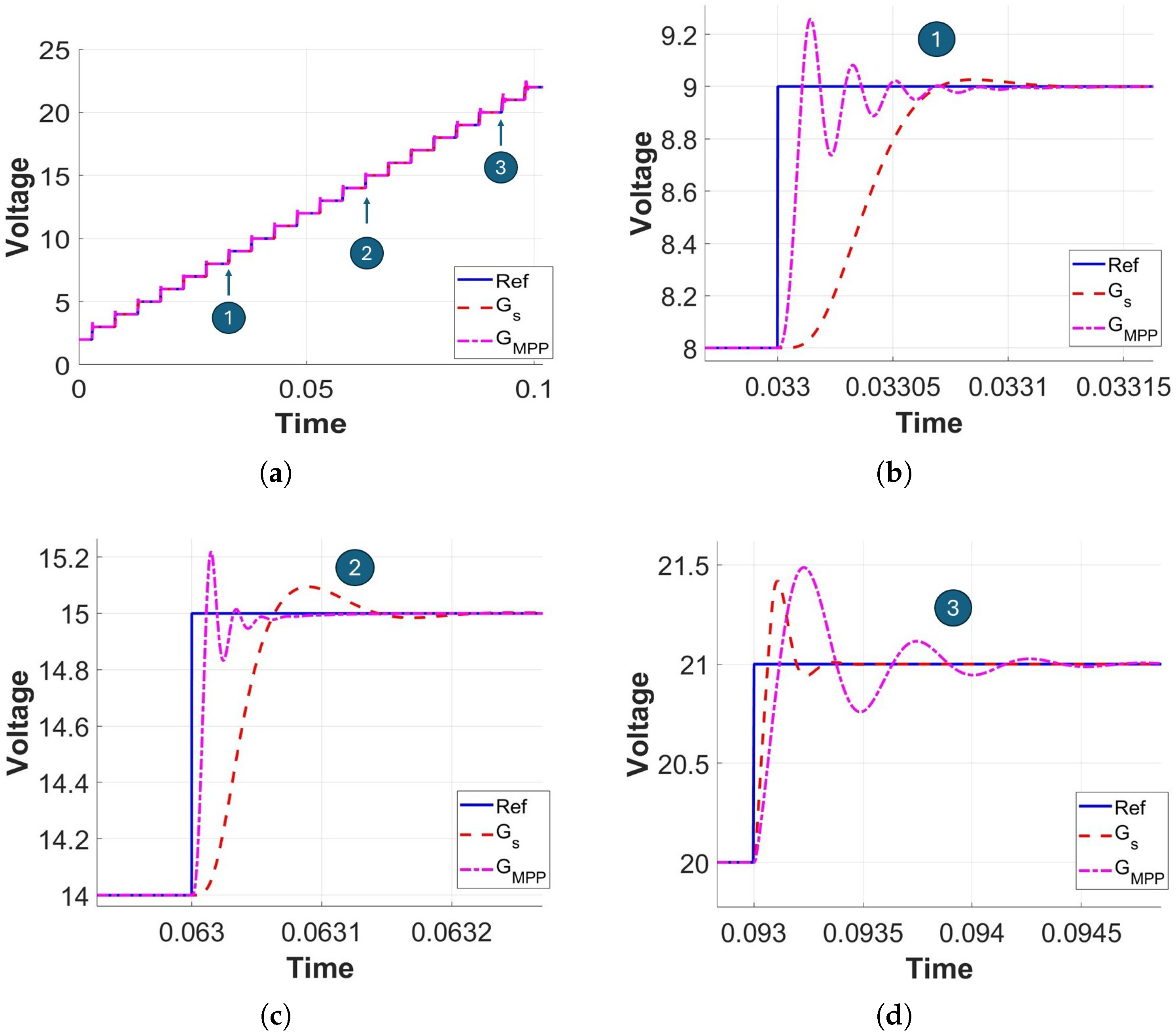
Figure 16 illustrates the performance of the gain-scheduled PI controller compared with a fixed PI controller tuned only at the maximum power point (denoted as
) for the boost converter. In the gain scheduling approach, the PI gains (
) were computed for different values of
, stored in a lookup table, and applied dynamically during operation. The reference step response (blue line) is compared against the closed-loop voltage trajectories of the gain-scheduled controller
(red dashed line) and the fixed controller
(magenta dash-dotted line).
From the overall response in
Figure 16a, it is evident that the gain-scheduled controller achieves tighter tracking of the reference voltage across the entire operating range, while the fixed controller tuned at
shows slower dynamics and larger deviations at points far from the nominal design condition. This clearly demonstrates the necessity of adapting the PI gains with respect to the operating point.
Figure 16b–d present zoomed-in views at three different voltage steps, labeled as regions 1, 2, and 3 in the overall plot. In
Figure 16b, corresponding to region 1, the fixed controller exhibits a sluggish rise time and noticeable steady-state error, whereas the gain-scheduled controller closely follows the reference with faster convergence. In
Figure 16c, corresponding to region 2, the superiority of the gain-scheduled design becomes more pronounced:
quickly stabilizes near the reference while
suffers from overshoot and a slower decay of oscillations. Finally, in
Figure 16d, corresponding to region 3, the fixed controller again displays significant oscillatory behavior and slower recovery, while the gain-scheduled controller maintains robustness with improved damping and reduced tracking error.
Overall, these results highlight the effectiveness of gain scheduling for boost converters operating over a wide input voltage range. By continuously adjusting and according to , the proposed gain-scheduled PI controller ensures consistent dynamic performance across all regions, whereas the fixed controller tuned at a single point () fails to provide uniform performance. This validates the importance of adopting gain scheduling strategies in practical PV converter applications, where the operating point is continuously varying due to irradiance and temperature fluctuations.
Table 6 provides a quantitative comparison between the fixed PI and gain-scheduled (GS) controllers in terms of rise time (
), settling time (
), and peak overshoot (
) for three representative voltage step responses. The results confirm that the GS controller achieves superior transient behavior and robustness compared to the conventional PI controller. Notably, the GS controller exhibits a substantial reduction in overshoot (from 2.77% to 0.22% in Step 1 and from 1.4% to 0.6% in Step 2) and shorter settling times, indicating improved damping and adaptability to varying PV operating points. Although the rise time of the GS controller is slightly higher in some cases, this corresponds to a smoother and more stable response, avoiding oscillations observed with the fixed PI controller. Overall, the gain-scheduled controller demonstrates enhanced dynamic stability and consistent performance across a wide range of PV operating conditions.
7. Conclusions
The proposed methodology integrates the dynamic behavior of the photovoltaic (PV) panel into the small-signal model of various DC–DC converters, providing a more realistic and precise representation of the overall system. Unlike traditional approaches that often overlook the input-side dynamics, this work introduces a valid and effective linearization strategy that accurately captures the true operating nature of PV–converter systems under different operating conditions.
A significant advancement of this study is the integration of the PV panel behavior into the small-signal representation, achieved by modeling the differential resistance for various operating points. This approach ensures physical consistency and enhances the accuracy of the derived small-signal models, particularly under open-circuit, short-circuit, and maximum power point (MPP) conditions. The study also presents the analytical derivation of the transfer function from duty cycle to input voltage, a perspective seldom explored in the literature. This formulation is critical for enhancing the responsiveness of converter control and enables better dynamic behavior analysis.
The study also highlights the benefits of gain scheduling applied to the Boost converter. By adapting the PI controller gains () at different PV operating points, the gain-scheduled controller achieves superior closed-loop performance compared to a fixed controller tuned solely at the MPP. This shows that the proposed modeling framework not only supports theoretical analysis but also facilitates the design of adaptive control strategies, improving stability, transient response, and overall energy harvesting efficiency.
However, despite these advancements, there are notable limitations in the current research. First, the model assumes ideal conditions for the PV module and converters, which may not fully capture the effects of practical system imperfections such as aging of PV cells and non-ideal switching behavior in converters. In addition, the study primarily focuses on linearized models, which may not accurately represent the system under highly nonlinear or transient operating conditions.
Furthermore, the control measures employed, such as gain scheduling and PI controllers, are effective but still rely on certain assumptions (e.g., predefined operating points). Real-world variations, such as fluctuating irradiance or temperature, may require more advanced adaptive control strategies to further optimize performance.
Future work should focus on addressing these limitations. Specifically, future extensions could incorporate more realistic models that account for non-idealities in both the PV module and converter hardware, as well as nonlinear behaviors during transient or fault conditions. Moreover, a comprehensive study of advanced control strategies such as model predictive control (MPC) or fuzzy logic controllers would provide more robust solutions for dynamic and unpredictable operating conditions. Thermal dynamics should also be integrated into the model to account for temperature-induced effects on both the PV panel and converters. In addition, future work will extend the experimental validation by incorporating the averaged differential resistance under varying irradiance and temperature conditions, providing a more comprehensive verification of the proposed model beyond fixed PV operating points. Finally, hardware-level validation and experimental testing are essential to confirm the model’s accuracy and its real-world applicability, ensuring the findings extend to diverse renewable energy systems and practical PV applications.
Overall, the modeling, control, and evaluation framework proposed in this work lays a strong foundation for improving the accuracy and reliability of DC–DC converter design in photovoltaic applications, while also opening up avenues for future advancements in both modeling and control systems.
