Abstract
As the integrated circuit process nodes are continuously reduced, higher complexity and accuracy requirements are imposed on the design rule checking (DRC) of standard cell layouts. Traditional manual repair methods are inefficient and prone to errors. A standard cell layout DRC automatic repair strategy based on an improved simulated annealing algorithm is proposed to address this issue. The proposed method quantifies the degree of graphic conflict by dynamically adjusting the annealing parameters; the high-conflict areas and repair paths are optimized. Meanwhile, the proposed method supports the repair of DRC rules at different process nodes ranging from MOSFET (28 nm) to FinFET (14 nm). Experiments results demonstrate that the proposed method outperforms traditional methods in both repair time and quality. Compared to manual repair, about 70% (MOSFET process) and 80% (FinFET process) of time can be saved by the proposed method, and new violations can be avoided during the repair process. Compared with traditional simulated annealing algorithms, approximately 40% (MOSFET process) and 50% (FinFET process) of the running time can be saved, and 100% elimination rate of DRC violations is achieved. The proposed method provides a fully automated and highly reliable DRC repair solution for integrated circuit layout design.
1. Introduction
The standard cell library serves as an important bridge for digital integrated circuits, and the layout design in its construction process is regarded as the most complex and time-consuming task [1,2,3,4,5,6]. This is mainly because the layout design has to adhere to extremely complex design rules, which are interdependent and interrelated [7,8,9,10]. Currently, the majority of existing technological solutions make attempts to address the DRC violation problem in standard cell layouts by employing more traditional methods. For instance, in some solutions, engineers are relied on to systematically check for violations in the layout and make manual adjustments based on their own experience. This approach is labor-intensive and prone to omissions for large-scale layouts [11,12,13,14]. There have also been some early automation attempts [13,14,15,16]. Although certain violations can be detected by these attempts, during the repair process, comprehensive consideration of complex layout structures and diverse design rules is lacking. As a result, new violations are introduced in the repaired layout, or the performance of other originally compliant areas is affected.
Some scholars have conducted research on the repair of DRC violations in circuit layouts. JINGUI LIN et al. focused on DRC hotspot prediction in VLSI design and proposed a serial deep learning model combining GCN and CNN to predict DRC violations during the layout stage [15]. Jun Zhang et al. proposed an adaptive RFID layout generator and DRC violation self-repair strategy, which decomposed the layout into polygon edges, introduced the concept of metal lines to record connection relationships, and then derived layout changes by specifying offsets to repair layout violations [16]. SASHANK M used Calibre_LV tool and TCL scripting language based on specific assumptions to fix DRC errors by searching for error layers, learning error types and distances, and moving error layers [17]. However, this strategy moves by deleting and recreating layers, which may lead to new DRC errors such as incorrect encapsulation of vias, size and resolution. Bongiovanni S proposed a repair process for DRC violations in the semi-custom layout under the ultra-deep sub-micron (UDSM) process, which automatically corrects the routing spacing, impedance and timing issues based on scripting [18]. But this method will cause a large area overhead.
It is concluded that there are few research papers on automatic repair of DRC violations in standard cell layouts, or the effects are not satisfactory. Thus, in this context, a standard cell layout DRC automatic repair strategy based on an improved simulated annealing algorithm is proposed, which is capable of achieving an efficient and accurate automatic repair of DRC violations in standard cell layouts. This strategy can intelligently identify various complex violations and fully consider the overall structure and design rules of the layout during the repair process, ensuring that the original performance and functionality of the layout are maintained to the greatest extent possible while eliminating DRC violations, providing a more reliable and efficient solution for standard cell layout design.
2. Design of DRC Automatic Repair Strategy Based on Improved Simulated Annealing Algorithm
2.1. Overall Framework
In standard cell layout design, Design Rule Check (DRC) is a critical step for ensuring that the layout complies with manufacturing process requirements. Comprehensive DRC violation checks on standard cell layouts are conducted using professional automation tools such as Calibre. Based on a series of pre-set design rules, including line width, spacing, and coverage, among others, the graphic elements in the layout are inspected one-by-one using these tools. Once all types of violations are identified, they are classified. Common types of violations are as follows: (1) Spacing violation: The distance between graphics is found to be less than the minimum spacing specified by the design rules. (2) Line width violation: The width of the metal is determined to be either less than or greater than the range permitted by the design rules. (3) Area violation: The area of the graphic is determined not to meet the requirements of the design rules. The overall design process is shown in Figure 1.
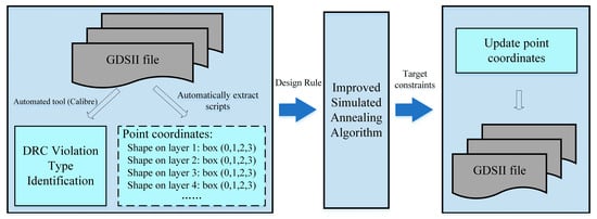
Figure 1.
Overall design process of DRC automatic repair.
2.2. Principle of Improved Simulated Annealing Algorithm
2.2.1. Basic Principle
In standard cell layout restoration, the objective is to have conflicts between graphics minimized and to ensure that the distances between all graphics are made to meet user-defined minimum distance constraints. During the algorithm’s operation, there will first be an inferior solution, which refers to the solution with a higher objective function value and more severe conflicts between graphs. Such solutions are usually accompanied by an intensification of DRC violations. For instance, suppose that there is an irregular spacing of metal wires in a certain layout (the actual spacing is 3 nm, which is less than the 5 nm required by the design rule). Through Equation (1), the objective function value of the algorithm in the current state can be calculated as E1 = 4.
If the algorithm generates a new state, causing the metal wire spacing to further reduce to 2 nm, at this time the objective function value becomes E2 = 9. This new state is an inferior solution, with more severe DRC violations and a higher objective function value. It is a solution that is not helpful for repairing the objective (eliminating DRC violations) or even has a counterproductive effect. Therefore, traditional simulated annealing algorithms will accept such inferior solutions with a certain probability, with the aim of avoiding getting trapped in local optima [19,20]. For instance, if there are still unrepaired errors near the current optimal solution, it is necessary to accept the inferior solution to break out of the local area and explore a better repair direction. The improved simulated annealing algorithm, through an adaptive temperature attenuation strategy, dynamically adjusts the probability of accepting an inferior solution, thereby more efficiently balancing global exploration and local convergence, and focusing on the optimal repair result. Among them, temperature refers to the control parameter T set by the algorithm in each round of iteration, which determines the probability of the algorithm accepting inferior solutions. The higher the temperature, the greater the probability of accepting the inferior solution, which is conducive to breaking away from the local optimum. The lower the temperature, the smaller the probability of accepting inferior solutions, and the algorithm tends to converge. Temperature decay, on the other hand, refers to the mechanism by which temperature gradually decreases during an iterative process, which is used to simulate the cooling stage in the physical annealing process. By reasonably setting the temperature attenuation strategy, the global exploration and local development capabilities of the algorithm can be balanced, and the convergence efficiency and the quality of the solution can be improved.
Therefore, the proposed improved simulated annealing algorithm adopts an adaptive temperature decay strategy to dynamically adjust the temperature decay coefficient based on the quality of the current solution and the number of iterations of the search, in order to better automatically repair DRC errors in standard cells.
2.2.2. Repair Mechanism Steps
- (1)
- Initialization
Refer to the GDS file of the standard cell layout using Klayout software and extract graphic information to form specific data point coordinates. Set parameters according to the formula, including initial temperature T0, termination temperature Tend, initial temperature decay coefficient α0, maximum iteration times itermax, and iteration times L for each temperature, adjust parameters α and γ. The explanation of important parameters as follows:
- Initial temperature T0: The initial temperature is an important parameter of the simulated annealing algorithm, which determines the randomness of the algorithm in the initial search stage. A higher initial temperature allows the algorithm to conduct a more extensive search in the solution space, avoiding premature entry into local optima. Generally, the appropriate initial temperature can be selected based on the scale and complexity of the problem. For example, for a smaller scale layout repair problem, set T0 to 100 first.
- Termination temperature Tend: The termination temperature indicates the condition for the algorithm to stop searching. When the temperature drops below the termination temperature, the algorithm considers that a good solution has been found and stops iterating. Usually, Tend is set to a smaller value, such as 0.1.
- Temperature attenuation coefficient α: The temperature attenuation coefficient controls the rate of temperature decrease. Its value is usually between 0 and 1, for example, α = 0.9 means that the temperature drops to 90% of its original level after each iteration. Note that α cannot equal 1. If α = 1, the temperature will never drop. The improved simulated annealing algorithm will continue to accept poor solutions with a high probability, unable to shift from global exploration to local convergence. It will always remain outside the optimal solution and thus fail to find the global optimal solution.
- The number of iterations L at each temperature: At each temperature, the algorithm will perform L iterations to fully explore the solution space at the current temperature. The value of L can be adjusted according to the complexity of the problem and can generally be set between 10 and 100.
- Initial solution generation: Randomly generate an initial solution x0, representing a layout of graphics in the layout. The initial solution can be generated by randomly moving or rotating the shape.
- Optimal solution initialization: Calculate the objective function value f(x0) of the initial solution and set the initial solution as the historical optimal solution xbest = x0 and the historical optimal objective function value fbest = f(x0). Record the minimum objective function value fmin = f(x0) and the maximum objective function value fmax = f(x0). Calculate the new temperature decay coefficient αnew based on the adaptive temperature decay formula:
Then update temperature T = αnewT.
- (2)
- Heuristic neighborhood solution generation
Calculate the number of conflicts between each graphic and other graphics. In a standard cell layout, a conflict refers to the situation where the geometric distance dij between any two figures i and j is less than the minimum spacing constraint dmin given by the user. Each time this situation occurs, the respective conflict counters increase by 1. Then sort the graphics in descending order of conflict frequency. In the generation of neighborhood solutions, priority is given to selecting graphics with more conflicts for position adjustment to generate new solutions x′. For example, add a random small offset to the x and y coordinates of the graph with the highest number of conflicts, such as a random number between [−0.1, 0.1].
- (3)
- Objective function calculation
Calculate the objective function values f(x) and f(x′) for the current solution x and the new solution x′, where objective function f(x) is defined as the number of conflicts between graphs that do not satisfy the minimum distance constraint:
Here, n is the number of graphics in the layout, dij is the distance between graphics i and j, and dmin is the minimum distance constraint defined by the design rules.
- (4)
- Acceptance of solution
Determine whether to accept the new solution based on the objective function values f(x′) and f(x) of the new solution x′ and the current solution x. If f(x′) < f(x), it means that the new solution is better than the current solution, and the new solution x′ is directly accepted as the current solution, that is, x = x′. If f(x′) ≥ f(x), then accept the new solution x′ with probability P.
Generate a random number γ between 0 and 1, if γ < P, then x = x′. Otherwise, the current solution remains unchanged. If f(x′) < fbest, it indicates that the new solution is the historically optimal solution. Update the historical optimal solution xbest = x′ and the historical optimal objective function value fbest = f(x′). And update fmin = min(fmin,f(x′)) and fmax = max(fmax,f(x′)).
If the objective function value of the current solution is worse than the historical optimal solution and the probability of accepting a new solution is low (such as P < 0.1), there is a certain probability of directly returning the historical optimal solution x = xbest to continue the search.
- (5)
- Update the number of iterations
The number of iterations iter = iter + 1 is updated, and after each iteration, the randomness of the algorithm gradually decreases, thereby allowing the algorithm to converge to a better solution.
- (6)
- End condition judgment
When T ≤ Tend or iter ≥ itermax occurs, the algorithm terminates, and the final solution becomes the historical optimal solution xbest. Otherwise, return to the neighborhood solution generation step and continue iterating.
2.2.3. Verification and Iteration of Repair Results
After the repair is completed, the automated DRC inspection tool is used again to check the repaired layout and verify the repair results. If DRC violations still exist, the above automatic repair process is repeated until all violations are fixed. In practical applications, a maximum number of iterations can be set to avoid the algorithm getting stuck in an infinite loop. The overall algorithm flow is shown in Figure 2.
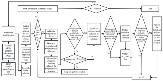
Figure 2.
Algorithm flowchart.
2.2.4. Complexity Analysis
- (1)
- Time complexity
The time complexity of improved simulated annealing algorithm mainly depends on the number of iterations and the computational complexity of the objective function. In each iteration, it is necessary to calculate the objective function value and the number of conflicts for each graph. The calculation of the objective function requires traversing all graph pairs, with a time complexity of O(n2), where n is the number of graphs. The total number of iterations depends on the initial temperature, termination temperature, and maximum number of iterations, usually denotes as O(itermax). Therefore, the overall time complexity of improving the simulated annealing algorithm is O(n2·itermax).
- (2)
- Space complexity
The main space overhead lies in storing graphic information, conflict frequency, and historical optimal solutions; therefore, the space complexity is O(n), where n is the number of graphics.
3. Results and Analysis
3.1. Application Design and Results
To verify the effectiveness and feasibility of the proposed DRC automatic repair method, a series of experiments were designed. And it runs on a Windows operating system with a CPU of 11th Gen Intel(R) Core(TM) i7-11700K and a frequency of 3.60 GHz. Standard cell layouts in the 28 nm MOSFET process and 14 nm FinFET process were utilized for DRC violation repair. In the experiment, the GDS file of the standard cell layout was input into an improved simulated annealing algorithm, which automatically fixed DRC violations through the algorithm. At the same time, different initial temperatures, temperature attenuation coefficients, and maximum iteration times are set to observe their effects on the repair effect. The proposed method can perform DRC violation repair on standard cell layouts compatible with multiple process structures.
- (1)
- MOSFET process
In the standard cell layout design stage of the MOSFET process, the layout may be drawn by the engineer due to a lack of understanding of the design rules, negligence, or improper use of design tools, resulting in non-compliance with the graphic size and spacing. Especially, owing to the large number of transistors, when the limit routing is pursued, the insufficient spacing of metal wires and the insufficient coverage of the metal layer to the contact hole are often caused, resulting in violations of less than the minimum spacing and minimum coverage of the metal. However, the minimum spacing of the metal is insufficient, which will cause the parasitic capacitance to increase and the signal crosstalk. Insufficient coverage of the metal layer to the contact hole will increase the contact resistance and reduce the connection reliability. In addition, between the AA (Active Area) and GT (Gate), the minimum distance from the AA edge to the GT edge will be ignored because of the pursuit of the minimum area, and the lack of spacing will lead to the increase in leakage current or transistor performance drift. These violations caused by human error or design tool accuracy problems are more common in the design stage. Table 1 shows the key DRC violation indicators and their impact for standard cell layout of MOSFET processes.

Table 1.
The key DRC Violations in the standard cell layout of the MOSFET process (28 nm) of a certain foundry, along with the impacts resulting from them.
The key indicators of DRC violations to verify the repair effect of the proposed method are shown in Table 1 to achieve. The algorithm parameters were set by setting the initial temperature to 100, the attenuation coefficient to 0.9, and the number of iterations to 30, and this parameter setting was also adopted in the experiments described later. A schematic diagram of the DRC violation in the standard cell layout based on the 28 nm process (taking the D flip—flop as an example) is shown in Figure 3a, and its repair schematic diagram is shown in Figure 3b. In the violation case of type (i), the minimum distance from the AA edge to the Gate edge is insufficient. Therefore, the coordinates of points a, b, c and d are moved in the negative direction of the X-axis so that the minimum spacing of 0.085 μm could be satisfied. For type (ii) violations caused by the metal layer covering the contact hole too small, points e and f were first attempted to be moved in the positive direction of the X-axis. It is found that the distance Dw between them and the metal on the right cannot meet the minimum distance rule, and the violation still exist. Therefore, the repair is carried out by moving vertically, that is, the coordinates of points f and g are moved towards the negative direction of the y-coordinate to increase the coverage area of the metal layer on the contact hole to reach more than 0.015 m2. In the violations of type (iii) caused by too small spacing between metal wires, the purple dashed box area is uniformly moved in the positive direction of the X-axis until the minimum spacing of the metal at 0.05 μm could be satisfied.
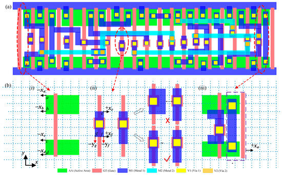
Figure 3.
The schematic diagram of the DRC violation repair of the standard cell layout based on the 28 nm process of a certain foundry: (a) Standard cell layout with DRC violations; (b) Repair process.
- (2)
- FinFET process
The FinFET process features three-dimensional structural characteristics. Besides the two-dimensional size requirements of the traditional plane, the dimensions and spacings in the vertical direction are also taken into account. Strict dimensional regulations are imposed on the Fin height, Fin spacing, and the structure of the gate surrounding the Fins of FinFET. If the Fin spacing is too small, the electrical performance of the transistor and the feasibility of the manufacturing process will be affected. Precise requirements are also imposed on the coverage size between the gate and the Fins in the vertical direction. If the coverage is insufficient or excessive, which will lead to abnormal electrical performance and result in violations of the graphic size and spacing related to the three-dimensional structure. The additional size and spacing constraints brought by this three-dimensional structure make the types of DRC violations in terms of graphic size and spacing in the stereoscopic FinFET process more complex and diverse. The key DRC violation indicators of the standard cell layout in the FinFET process and the resulting impacts are presented in Table 2.
Table 2.
The key DRC Violations in the standard cell layout of the FinFET process (14 nm) of a certain foundry, along with the impacts resulting from them.
A schematic diagram of the standard cell layout of a 14 nm process in a certain foundry (taking the D flip—flop as an example) is shown in Figure 4, where the layout with DRC violations is presented in Figure 4a, and the schematic diagram of DRC repair is shown in Figure 4b. Compared with the MOSFET process, the FinFET process has more requirements for the definition of Fin and the design of its AA region width. However, other key DRC violation indicators are the same as those of the MOSFET, and the repair process is also identical, so they will not be described again. In the standard cell layout design of the FinFET process, violations are often caused by too small Fin spacing, which simultaneously results in the width of the AA not being met. Therefore, the proposed method will increase the spacing of the fins (moving in the negative direction of the Y-axis) according to the design rule (DFin = 0.038 µm), and then the width of the AA will also increase. Eventually, the extra Fin due to the increased spacing will be deleted.
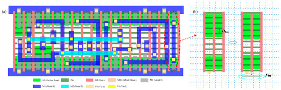
Figure 4.
The schematic diagram of the DRC violation repair of the standard cell layout based on the 14 nm FinFET process of a certain foundry: (a) Standard cell layout with DRC violations; (b) Repair process.
After the proposed method is repaired, the industry standard tool Calibre is used to check the design rules to ensure that there are no violations, thereby guaranteeing that the layout fully complies with the design rule requirements.
3.2. Comparative Analysis of Repair Efficiency
In the illustration of DRC violation repair for the standard cell layout in Section 3.1, only some common DRC violations are presented. In fact, all kinds of DRC violations can be repaired automatically. Moreover, the proposed method has a significant advantage over the traditional methods in the DRC repair time of standard cell layouts. Compared with the time taken by experienced layout engineers to repair the same type of DRC errors, the proposed method can save about 70% (MOSFET process) and 80% (FinFET process) of time. Compared with the operation time of the traditional simulated annealing algorithm, approximately 40% (MOSFET process) and 50% (FinFET process) of the time can be saved by it. The specific comparison situation is shown in Table 3.
Table 3.
Comparison of DRC violation repair for standard cell layouts of MOSFET and FinFET processes.
4. Conclusions
An automatic repair strategy for DRC in standard cell layouts is proposed. Based on the improved simulated annealing algorithm, efficient and accurate repair of DRC violations is achieved through an adaptive temperature attenuation strategy and a heuristic neighborhood solution generation method. In terms of algorithm improvement, an adaptive temperature attenuation strategy is adopted, and the temperature attenuation coefficient is dynamically adjusted, whereby the convergence speed and global search ability of the algorithm are improved. The heuristic neighborhood solution generation method is introduced to give priority to handling the graphics with a high number of conflicts, significantly improving the repair efficiency. The proposed method was tested on the standard cell layouts of the MOSFET process (28 nm) and the FinFET process (14 nm), verifying the adaptability of the algorithm to different process nodes, and the violation elimination rate could reach 100%. Compared with traditional manual repair, the proposed method can save approximately 70% (MOSFET process) and 80% (FinFET process) of the time. Compared with the traditional simulated annealing algorithm, approximately 40% (MOSFET process) and 50% (FinFET process) of the running time are saved, and a better repair effect is obtained. It is demonstrated that the proposed method can provide an automated solution for integrated circuit layout design, significantly reducing the repair cost while ensuring the repair quality. Moreover, it can also be applied to complex layout structures and diverse design rules, as well as more advanced processes. We expect that it will be extended to the repair of DRC violations in other types of circuit layouts in the field of integrated circuits due to the strong practicality and promotion value.
Author Contributions
Conceptualization, W.H., B.L., W.L. and Z.W.; Methodology, W.H., Z.L. and S.H.; Writing—original Draft, W.H.; Writing—review and editing, B.L., W.L., Z.W., Z.L., S.H. and C.Q. All authors have read and agreed to the published version of the manuscript.
Funding
This work was supported by the Guangdong S&T Programme, China (2022B0101180001).
Data Availability Statement
The original contributions presented in the study are included in the article, further inquiries can be directed to the corresponding author.
Conflicts of Interest
Author Wenchao Liu and Chaozheng Qin were employed by the Guangzhou Primarius Electronic Technologies Co., Ltd., Guangzhou, China. The remaining authors declare that the research was conducted in the absence of any commercial or financial relationships that could be construed as a potential conflict of interest.
References
- Marinberg, H.; Garzón, E.; Noy, T.; Lanuzza, M.; Teman, A. Efficient implementation of many-ported memories by using standard-cell memory approach. IEEE Access 2023, 11, 94885–94897. [Google Scholar] [CrossRef]
- Carvalho, M.; Nunes, C.; Canal, B.; Puricelli, L.; Reinicke, L.; Webber, G.; Neutzling, A.; Altieri, M.; Conto, E.; Nagel, T.; et al. Standard Cell Library Validation Methodology. 2016. Available online: https://www.researchgate.net/publication/318467496_Standard_Cell_Library_Validation_Methodology (accessed on 1 October 2025).
- Afonso, R.; Rahman, M.; Tennakoon, H.; Sechen, C. Power efficient standard cell library design. In Proceedings of the 2009 IEEE Dallas Circuits and Systems Workshop (DCAS), Richardson, TX, USA, 4-5 October 2009. [Google Scholar]
- Hesham, A.R.; Nassar, A.; Mostafa, H. Design and implementation of energy-efficient near-threshold standard cell library for IoT applications. AEU-Int. J. Electron. Commun. 2021, 139, 153907. [Google Scholar] [CrossRef]
- De Carvalho, M.; Canal, B.; Puricelli, L.; Reinicke, L. Standard Cell Library Validation Methodology. In Proceedings of the Workshop Circuits and Systems, Belo Horizonte, Brazil, 29 August–3 September 2016. [Google Scholar]
- Xu, X.; Shah, N.; Evans, A.; Sinha, S.; Cline, B.; Yeric, G. Standard cell library design and optimization methodology for ASAP7 PDK. In Proceedings of the 2017 IEEE/ACM International Conference on Computer-Aided Design (ICCAD), Irvine, CA, USA, 13-16 November 2017. [Google Scholar]
- Tegazzini, L.; Di Meo, G.; De Caro, D.; Strollo, A.G.M. High-Precision mux-Based Digital Delay Interpolators Based on a Novel Transistor Sizing Algorithm. IEEE Trans. Circuits Syst. II Express Briefs 2025, 72, 938–942. [Google Scholar] [CrossRef]
- Wang, J.; Wong, A.K.; Lam, E.Y. Standard cell layout with regular contact placement. IEEE Trans. Semicond. Manuf. 2004, 17, 375–383. [Google Scholar] [CrossRef]
- Li, H.; Lee, R.; Lee, T.; Xue, T.; Liu, H.; Wu, H.; Wan, Q.; Du, C.; Hu, X.; Liu, Z. An efficient way of layout processing based on calibre DRC and pattern matching for defects inspection application. In Proceedings of the Design-Process-Technology Co-Optimization for Manufacturability XII, San Jose, CA, USA, 28 February–1 March 2018; SPIE: Washington, DC, USA, 2018; Volume 10588, pp. 282–287. [Google Scholar]
- Huang, L.; Yang, L.; Kan, H.; Zou, E.; Wan, Q.; Du, C.; Hu, X.; Liu, Z. Using pattern based layout comparison for a quick analysis of design changes. In Proceedings of the Design-Process-Technology Co-optimization for Manufacturability XII, San Jose, CA, USA, 28 February–1 March 2018; SPIE: Washington, DC, USA, 2018; Volume 10588, pp. 276–281. [Google Scholar]
- van Staden, R.; Delport, J.A.; Coetzee, J.A.; Fourie, C.J. Layout versus schematic with design/magnetic rule checking for superconducting integrated circuit layouts. In Proceedings of the 2019 IEEE International Superconductive Electronics Conference (ISEC), Riverside, CA, USA, 28 July–1 August 2019; IEEE: New York, NY, USA, 2019; pp. 1–3. [Google Scholar]
- Cao, R.; Ferguson, J.; Drissi, Y.; Gays, F.; Arriordaz, A.; O’Connor, I. DRC challenges and solutions for non-Manhattan layout designs. In Proceedings of the 2014 International Conference on Optical MEMS and Nanophotonics, Glasgow, UK, 17–21 August 2014; IEEE: New York, NY, USA, 2014; pp. 175–176. [Google Scholar]
- Kabeel, A.; Kim, S.; Park, Y.G.; Kim, D.; Kwan, J.; Rizk, S.; Madkour, K.; Shafee, M.; Kim, J. Design rule manual and DRC code qualification flows empowered by high coverage synthetic layouts generation. In Proceedings of the DTCO and Computational Patterning II, San Jose, CA, USA, 27 February–2 March 2023; SPIE: Washington, DC, USA, 2023; Volume 12495, pp. 415–428. [Google Scholar]
- Dai, V.; Yang, J.; Rodriguez, N.; Capodieci, L. DRC Plus: Augmenting standard DRC with pattern matching on 2D geometries. In Proceedings of the Design for Manufacturability through Design-Process Integration, San Jose, CA, USA, 28 February–2 March 2007; SPIE: Washington, DC, USA, 2007; Volume 6521, pp. 98–109. [Google Scholar]
- Lin, J.; Lin, W.; Liang, S.; Gao, P.; Xing, Y.; Wu, T.; Xiong, X.; Cai, S. An Efficient Method of DRC Violation Prediction with a Serial Deep Learning Model. ACM Trans. Des. Autom. Electron. Syst. 2024, 29, 1–16. [Google Scholar] [CrossRef]
- Zhang, J.; Meng, X.; Ming, F. An Adaptive RFIC Layout Generator with DRC Violations Self-repair Strategy. In Proceedings of the 2023 IEEE MTT-S International Wireless Symposium (IWS), Qingdao, China, 14–17 May 2023; IEEE: New York, NY, USA, 2023; pp. 1–3. [Google Scholar]
- Sashank, M. Automated DRC Error Solver for LVS Clean Layouts. Ph.D. Thesis, Indian Institute of Technology Madras Chennai, Chennai, India, 2021. [Google Scholar]
- Bongiovanni, S. Design Techniques for Secure Cryptographic Circuits in Deep Submicron Technologies. Available online: https://tesidottorato.depositolegale.it/handle/20.500.14242/98985 (accessed on 1 October 2025).
- Rutenbar, R.A. Simulated annealing algorithms: An overview. IEEE Circuits Devices Mag. 1989, 5, 19–26. [Google Scholar] [CrossRef]
- Yu, C.H.; Tsai, J.; Chang, Y.T. Intelligent Path Planning for UAV Patrolling in Dynamic Environments Based on the Transformer Architecture. Electronics 2024, 13, 4716. [Google Scholar] [CrossRef]
Disclaimer/Publisher’s Note: The statements, opinions and data contained in all publications are solely those of the individual author(s) and contributor(s) and not of MDPI and/or the editor(s). MDPI and/or the editor(s) disclaim responsibility for any injury to people or property resulting from any ideas, methods, instructions or products referred to in the content. |
© 2025 by the authors. Licensee MDPI, Basel, Switzerland. This article is an open access article distributed under the terms and conditions of the Creative Commons Attribution (CC BY) license (https://creativecommons.org/licenses/by/4.0/).