Abstract
During orbital operations, spaceborne microstrip antennas are continuously exposed to solar radiation and the cold thermal sink of space, enduring extreme temperature variations. These extreme temperature variations induce significant thermal stress, which leads to deformation in spaceborne antennas, inevitably degrading their operational performance. To address this issue, an optimized design method for antenna array structure based on strain compensation is proposed in this paper. The proposed method uses the COMSOL Multiphysics 6.2 to analyze thermal-structural-electromagnetic coupling behavior of spaceborne microstrip arrays under extreme temperature conditions. The simulation quantifies the thermal-strain distribution. Accordingly, different slits are introduced in regions of high-strain concentration, effectively redistributing the strain to minimize thermal deformation. This optimized configuration maintains superior electrical performance while significantly enhancing thermal stability. Both simulation and measurement results verify the effectiveness of the proposed optimization design method. Notably, the proposed method offers a novel solution for mitigating thermal-induced performance degradation in spaceborne antenna systems without requiring active thermal control.
1. Introduction
CubeSats are low-cost, cube-shaped nano-satellites designed for educational purposes originally [1]. The QN50 CubeSat program adopts a standard 1U satellite with a size of 10 cm × 10 cm × 10 cm, and a mass not exceeding 1.33 kg. With the continuous advancement of space technology, CubeSats have also sparked widespread interest in other fields, such as remote sensing, deep-space communications, and space exploration [2]. Their development trend has progressively shifted from the S-band to the X-band and further to the Ka-band. This poses higher requirements for antenna design in the Ka-band frequency range. In addition to the excellent electric performance, CubeSats require antennas installed on their outer surface to be easy to deploy, and to meet the requirements: low weight (≤50 g), thin thickness (≤5 mm), and small size (≤90 mm × 90 mm) [3]. Thermal stability is another critical factor in CubeSats antenna design [4]. As is well known, CubeSats operating in low Earth orbit (LEO) are subjected to prolonged solar radiation and extreme cold from the space environment [5]. The ambient temperature around the antenna arrays can vary from −160 °C to 120 °C [6,7]. Under such extreme temperature conditions, structural deformation of antenna elements due to thermal stress becomes inevitable, which ultimately degrades the electrical performance of the array. This issue is especially critical for Ka-band antennas, whose electrical performance is highly sensitive to physical deviations caused by deformation and stress.
Many scholars have proposed various solutions to address the issue of antenna thermal deformation. Analytical models for thermal analysis have been introduced to predict thermal deformation, such as the dual model theory [8], classical lamination theory combined with Eshelby’s equivalent inclusion method and Mori–Tanaka’s mean-field method [9], temperature penetration models for antenna structures [10], and related methods [11,12,13,14]. Most of these models rely heavily on principles of equivalence and simplification, which limits their applicability. To enhance the universality and accuracy of thermal analysis, multi-physics modeling methods have been developed, including structural-electromagnetic-thermal coupling techniques [15,16] and thermal–mechanical coupling approaches [17,18,19]. These multi-physics models enables detailed analysis of the influence of key factors on thermal deformation. Meanwhile, multi-physics simulation methods for thermal deformation analysis are presented in [20,21,22], and various experimental methods also are provided in [23,24,25].
Subsequently, genetic algorithms have been applied to optimize performance parameters [26,27]. However, these studies do not offer practical solution for correcting thermal deformation after it has occurred. Subsequently, thermal compensation methods have been proposed to mitigate performance degradation caused by thermal deformation. These compensation methods fall into two categories: electrical compensation and structural compensation. Electrical compensation methods restore electromagnetic performance by adjusting the array phase difference using phased shifters, metasurfaces, or metamaterials [28,29]. Such methods, however, require additional hardware and are more effective for large deformations than for small ones. Structural compensation methods, in contrast, are more suitable for small deformations. For instance, controllable bending moments can be generated through heating to counteract thermal deformation [26]. Another approach is structural compensation methods. Active structural compensation works by introducing a precisely controlled reverse mechanical deformation to counteract thermal effects. However, this approach tends to be complex, as it requires power supplies and control circuits, which also increase overall weight and cost [30,31]. Passive structural compensation relies on the inherent smart properties of the material or structure itself, making its design and optimization particularly challenging. Nevertheless, the implementation of these structural compensation methods is relatively complex.
This paper proposes an optimized structural design method for antenna array based on strain compensation. The method begins with an analysis of multi-physics field effects under extreme temperatures. To mitigate the resulting thermal deformation, a strategic slit design is introduced to redistribute the strain field. The optimization of the slit’s parameters is then undertaken using the White Shark Optimization (WSO) algorithm [32]. It offers a novel approach to mitigating thermal-induced performance degradation in spaceborne antenna systems without requiring active thermal control. The main contributions of the manuscript are as follows: (1) In contrast to traditional structural compensation methods, the proposed approach does not rely on additional equipment for shape adjustment, making it simpler and easier to implement; (2) The proposed method combines the multi-physics modeling and analysis method and WSO optimization algorithm to analyze multiple physical fields and generate an optimal structural design. Owing to its few adjustable parameters, the WSO algorithm is easy to implement, while simultaneously maintaining an effective equilibrium between global exploration and local exploitation; (3) the antenna is heated in air and its electrical parameters are measured, indirectly validating the effectiveness of the proposed method.
2. Spaceborne Microstrip Antenna Array
2.1. Antenna Element
A microstrip antenna element operating at 36 GHz is designed for spaceborne applications. The antenna architecture comprises three main layers. Figure 1a,b illustrate the top and side views of the antenna element, respectively. The top layer contains a rectangular copper radiating patch with a thickness of Hp = 0.035 mm, which is integrated with a quarter-wavelength impedance transformer and a 50 Ω microstrip feedline. As detailed in Table 1, the sizes of the patch are Lp = 2.58 mm and Wp = 2.5 mm; the sizes of the impedance transformer are Lq = 1.4 mm and Wq = 0.18 mm; and the sizes of the microstrip transmission line are Lm = 0.72 mm and Wm = 0.2 mm. To achieve circular polarization, the two top corners of the radiating patch are truncated with a side length of S = 0.34 mm. The middle layer is a Rogers 5880 substrate with sizes Ls × Ws × Hs, featuring a dielectric constant of 2.2 and a loss tangent of 0.0004. The bottom layer serves as a ground plane and is also fabricated from 0.035 mm-thick copper. The thermal parameters of the material used in the antenna element are provided in Table 2.
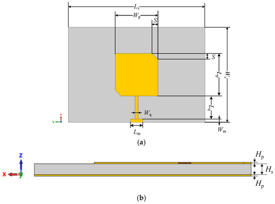
Figure 1.
Spaceborne microstrip antenna element structure: (a) Top view; (b) Side view.

Table 1.
Structural sizes of the antenna element (unit: mm).

Table 2.
Thermal parameters of the material used in the antenna element.
2.2. Antenna Array
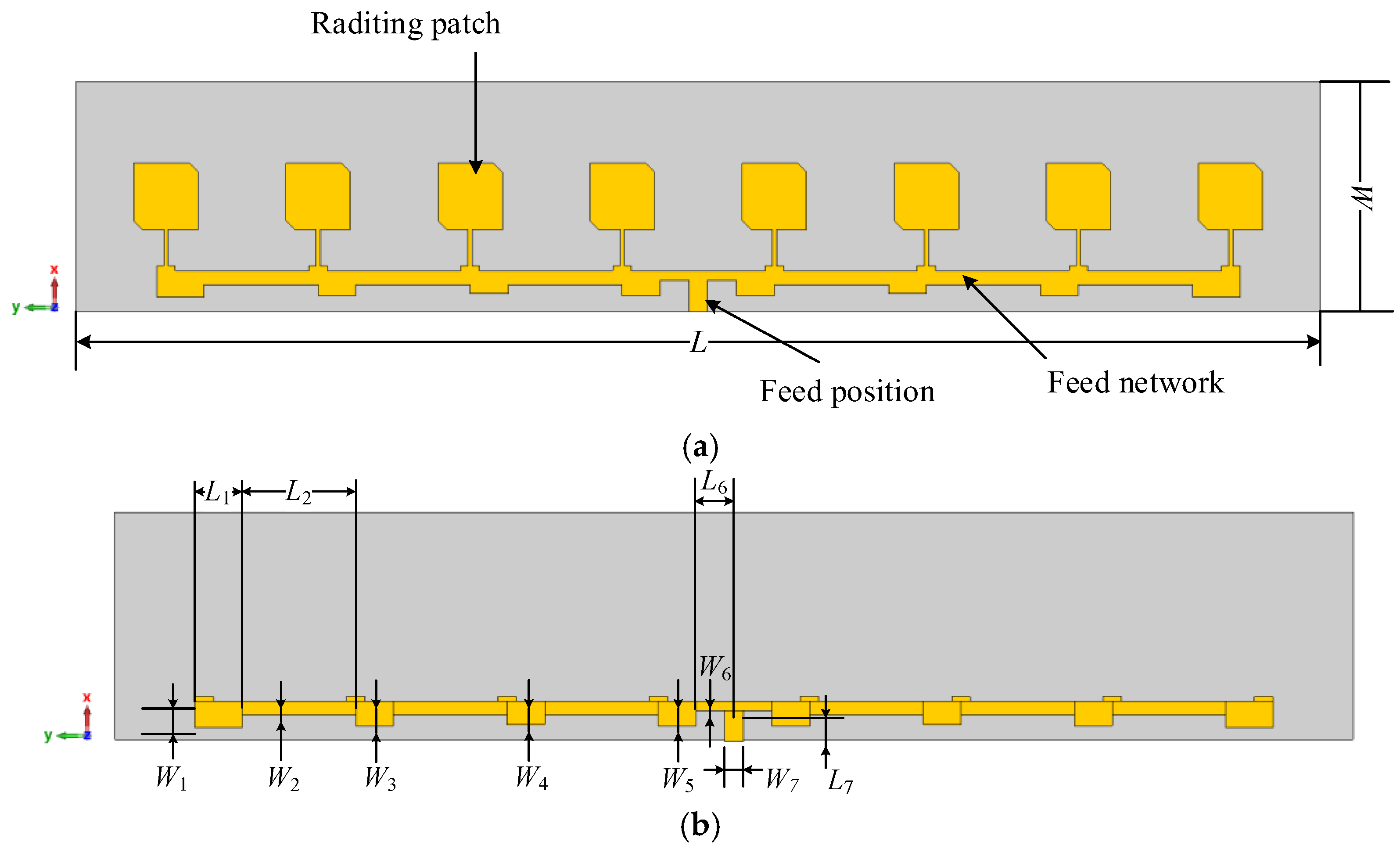
A Spaceborne microstrip antenna array is composed of eight of the aforementioned elements arranged in a linear configuration, as shown in Figure 2a. The overall sizes of the array are 48.44 mm × 8.92 mm × 0.32 mm. The structure of the feed network is illustrated in Figure 2b, with its sizes are presented in Table 3. The Chebyshev synthesis method [4] is used to determine the amplitude and phase of each antenna element, thereby achieving an optimal array radiation pattern. The excitation current amplitude ratio of the four antenna elements from the center to the edge in the feed network is calculated as follows:
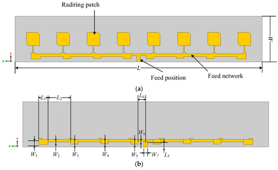
Figure 2.
Spaceborne microstrip antenna array: (a) Array structure; (b) Feed network structure.

Table 3.
Structural sizes of feed network (unit: mm).
To achieve high gain and low sidelobe, the antenna array is designed for a sidelobe level (SLL) below −15 dB.
2.3. Performance Analysis of Antenna Array
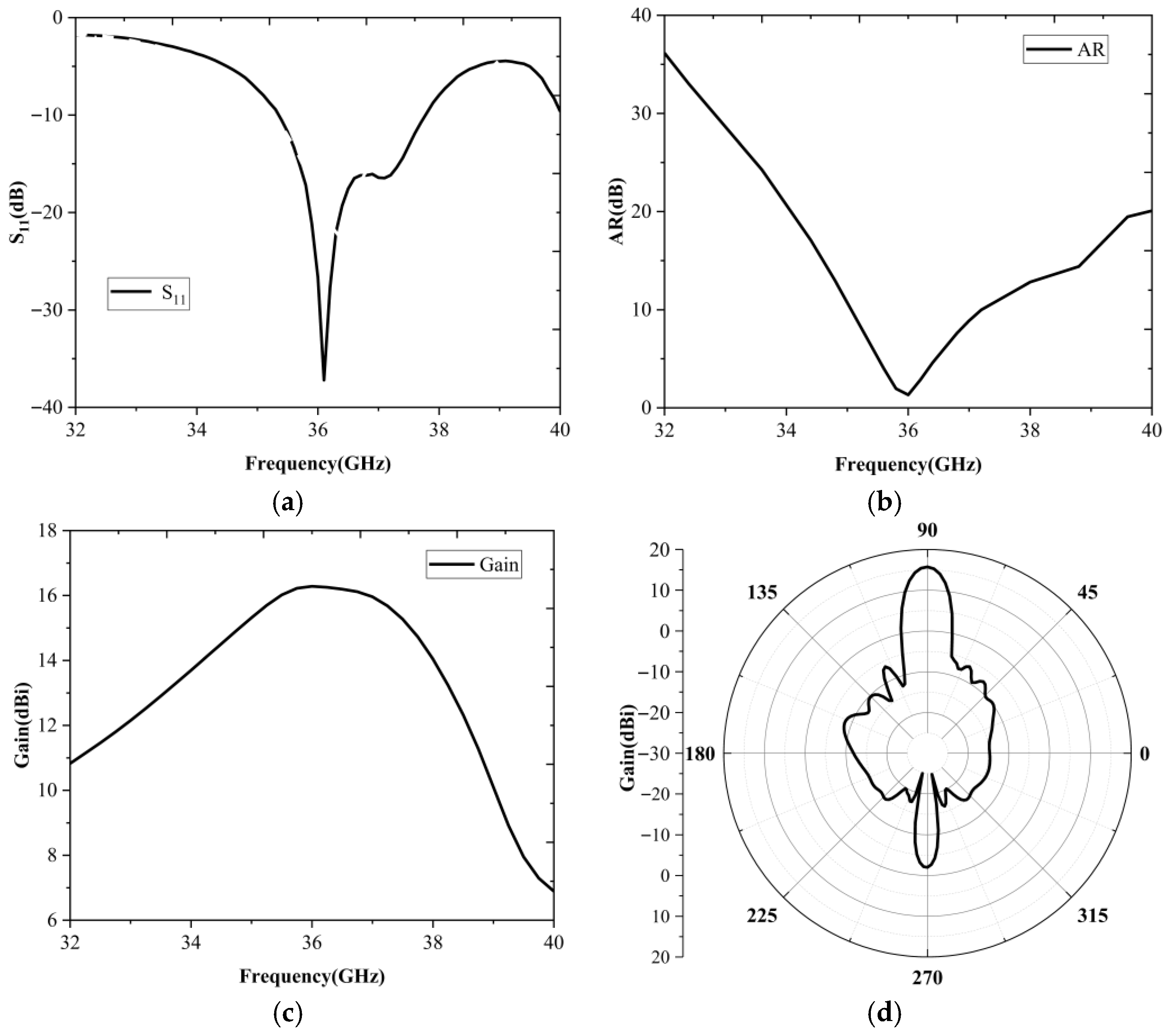
The COMSOL software is employed to simulate the electric performance of the spaceborne antenna array. The results are presented in Figure 3. As shown in Figure 3a, the reflection coefficient (S11) of the array is below −10 dB across the frequency band from 35.35 to 37.76 GHz. At the center frequency of 36 GHz, S11 reaches −26.57 dB. Figure 3b indicates that the axial ratio (AR) remains below 3 dB within the 35.69–36.19 GHz band. At 36 GHz, the AR is 1.54 dB, corresponding to an absolute AR bandwidth of 0.5 GHz and a relative AR bandwidth of 1.39%. Furthermore, Figure 3c,d show the variation of the gain with frequency and angle θ, respectively. A peak gain of 16.22 dBi is achieved. The radiation pattern in the φ = 90° plane exhibits a well-defined main lobe and side lobes, with a sidelobe level of −22.1 dB, which satisfies the design requirement of SLL < −15 dB.
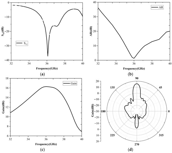
Figure 3.
Electrical parameters of the original array: (a) S11; (b) AR; (c) Gain; (d) Radiation pattern at φ = 90°.
The electric field distribution at 36 GHz is shown in Figure 4. The radiation pattern of the array exhibits symmetry, with the strongest radiation intensity occurring in the center elements and decreasing progressively towards the edges. pattern arises from the This uniform distribution is a direct result of the non-uniform currents excitation across the array elements.
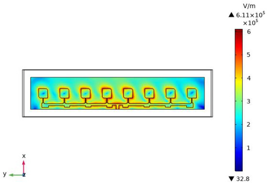
Figure 4.
Electric field distribution.
3. Multi-Physics Fields Analysis of Designed Spaceborne Microstrip Antenna Array
Spaceborne microstrip antenna arrays may deform under extreme temperature conditions, which can lead to performance degradation. This process is the result of the coupling effect of multi-physical fields. In this study, the COMSOL software is used to simulate the multi-physics field effects of the microstrip antenna array. The electromagnetic field, solid heat transfer, and solid mechanics modules in COMSOL are used to co-simulate.
3.1. Solid Thermal Model
The governing equation for thermal analysis is as follows:
where ρ is the density; c is the specific heat capacity; λ is the thermal conductivity; T is temperature; t is time; Q is the thermal source.
In the Solid Heat Transfer module of the COMSOL, the outer surface of the array is set as a “Surface-to-Ambient Radiation” boundary condition, simulating the thermal radiation experienced in space. The initial reference temperature is set to 20 °C, while the ambient environmental temperature is defined as either 120 °C or −160 °C. The surface emissivity is set to either 0.6 or 0.4.
3.2. Solid Mechanical Model
The governing equation for mechanics analysis is as follows:
where [σ] and [ε] are the stress tensor and strain tensor, respectively; σii(i=x,y,z) refers to the normal stress; τij(i=x,y,z;j=x,y,z) refers to the shear stress; εii(i=x,y,z) refers to the normal strain; γij(i=x,y,z;j=x,y,z) refers to the shear strain; u, v, w refer to the displacement components in different directions; [D] is elastic matrix; ε0 is the thermal strain; α is the coefficient of thermal expansion, and ΔT is the temperature change (the temperature difference between the initial and final states).
In the Solid Mechanical module of the COMSOL, the array material is defined as linear elastic. A fixed constraint boundary condition is applied to both ends of the array.
3.3. Electromagnetic Field Model
The governing equation for electromagnetics analysis is as follows:
where εe denotes the dielectric constant, and µ is the magnetic permeability respectively, J is the current density, E is the electric field.
In the Electromagnetic Wave module of the COMSOL, a radiation boundary condition is applied to the exterior boundaries to simulate free space.
3.4. Multi-Physics Fields Analysis
Multi-physics field analysis of the microstrip antenna array is performed by the COMSOL under both high and low temperature conditions. The unstructured finite element mesh is shown in Figure 5. The maximum and minimum element sizes are set to 5.26 mm and 0.947 mm, respectively.

Figure 5.
Finite element mesh.
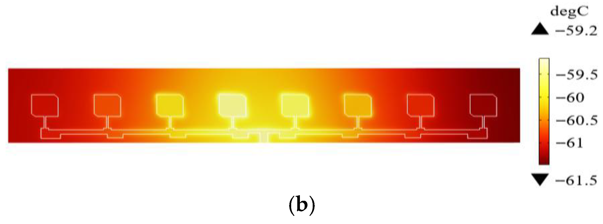
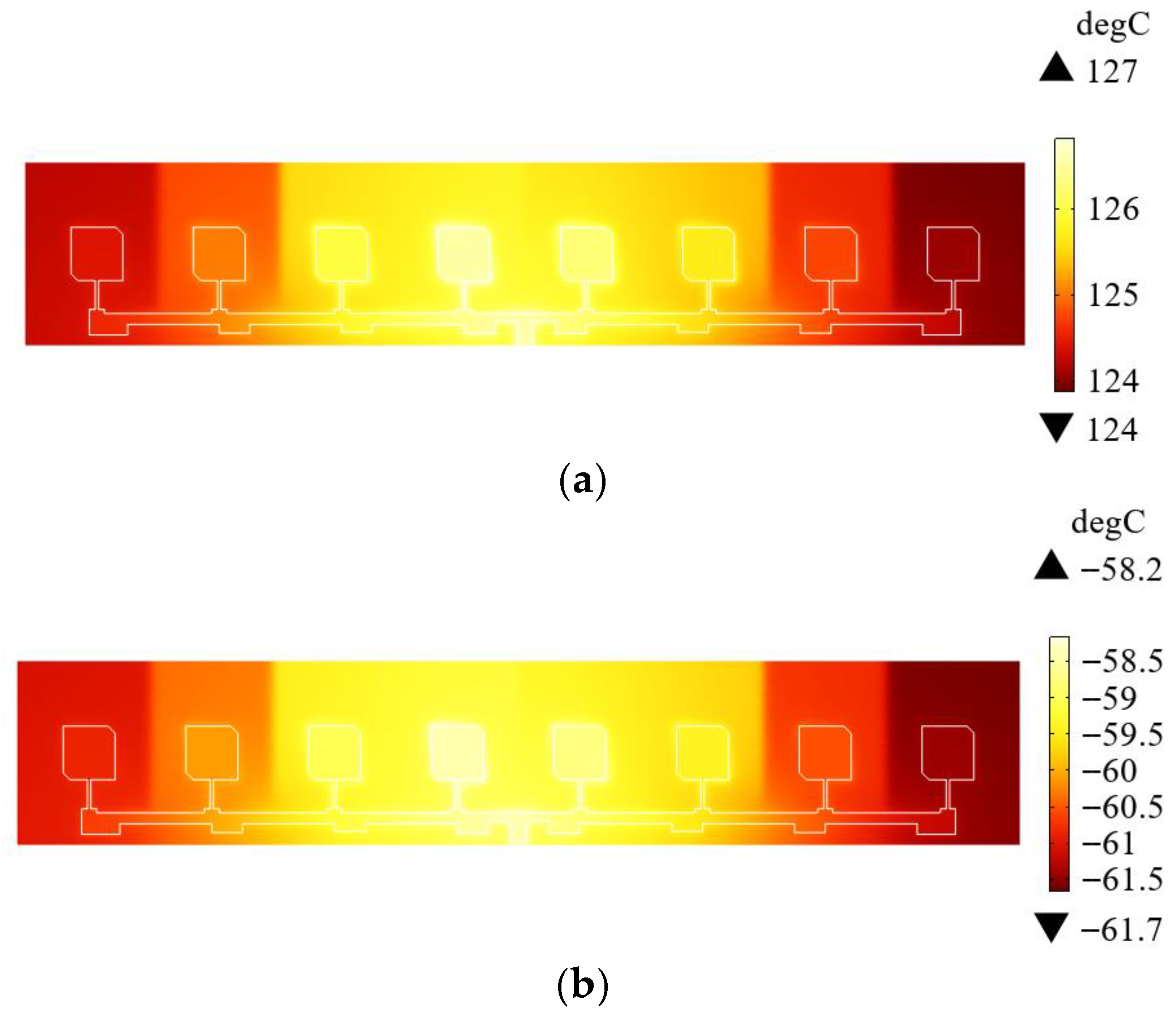
The steady-state temperature distributions are shown in Figure 6. It can be seen that the temperature distribution characteristics: (1) The distribution is symmetrical, decreasing from the center towards both sides—a pattern analogous to the electric field distribution observed earlier. (2) Under a high-temperature ambient condition of 120 °C, the maximum array temperature reaches 126 °C, while in a low-temperature environment of −160 °C, it attains −57.57 °C This behavior results from internal electromagnetic power dissipation within the array. (3) The radiating patch exhibits a slightly higher temperature than the dielectric substrate, due to its significantly higher thermal conductivity (400 compared to 0.2 for the substrate).
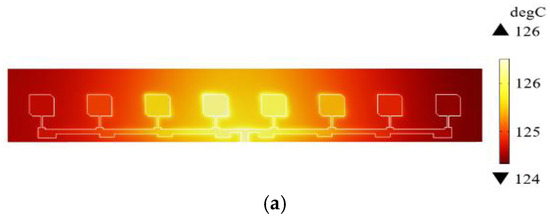

Figure 6.
Temperature distribution of the original array: (a) High temperature; (b) Low temperature.
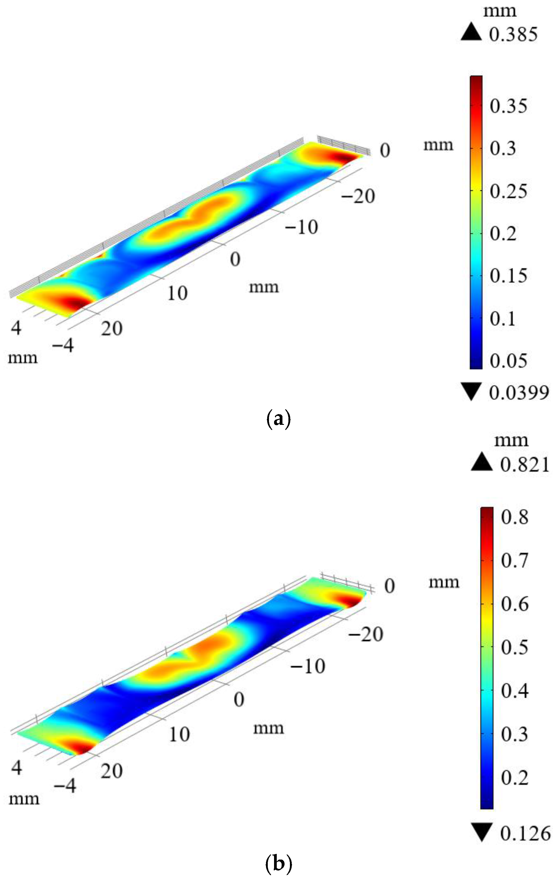
Figure 7 shows the steady-state strain distribution of the array under high and low temperature conditions. As observed in Figure 7a, the overall structure of the array deforms into an upward convex shape. The maximum deformation is 8.89 mm occurs at the center of the array, decreasing toward both ends, where the minimum deformation is 0.04 mm. At an ambient temperature of 120 °C, the array undergoes thermal expands. Since the thermal expansion coefficient of the dielectric substrate is greater than that of the copper ground plate, the upper dielectric substrate expands more significantly than the lower ground plate. As the ground plate constrains downward expansion of the substrate, the array deforms into an upward convex shape.
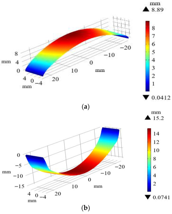
Figure 7.
Strain distribution of the original array: (a) High temperature; (b) Low temperature.
As seen from Figure 7b, the overall structure of the array deforms into a concave shape. The maximum deformation is 15.2 mm occurs at the center of the array, and decreases toward both ends, where the minimum deformation is 0.074 mm. At the ambient temperature reaches −160 °C, the array experiences thermal contraction. The thermal expansion coefficient of the dielectric substrate is greater than that of the copper ground plate; thus, the upper dielectric substrate contracts more significantly than the lower ground plate. The resulting concave deformation occurs as the ground plate constrains the upward contraction of the substrate.
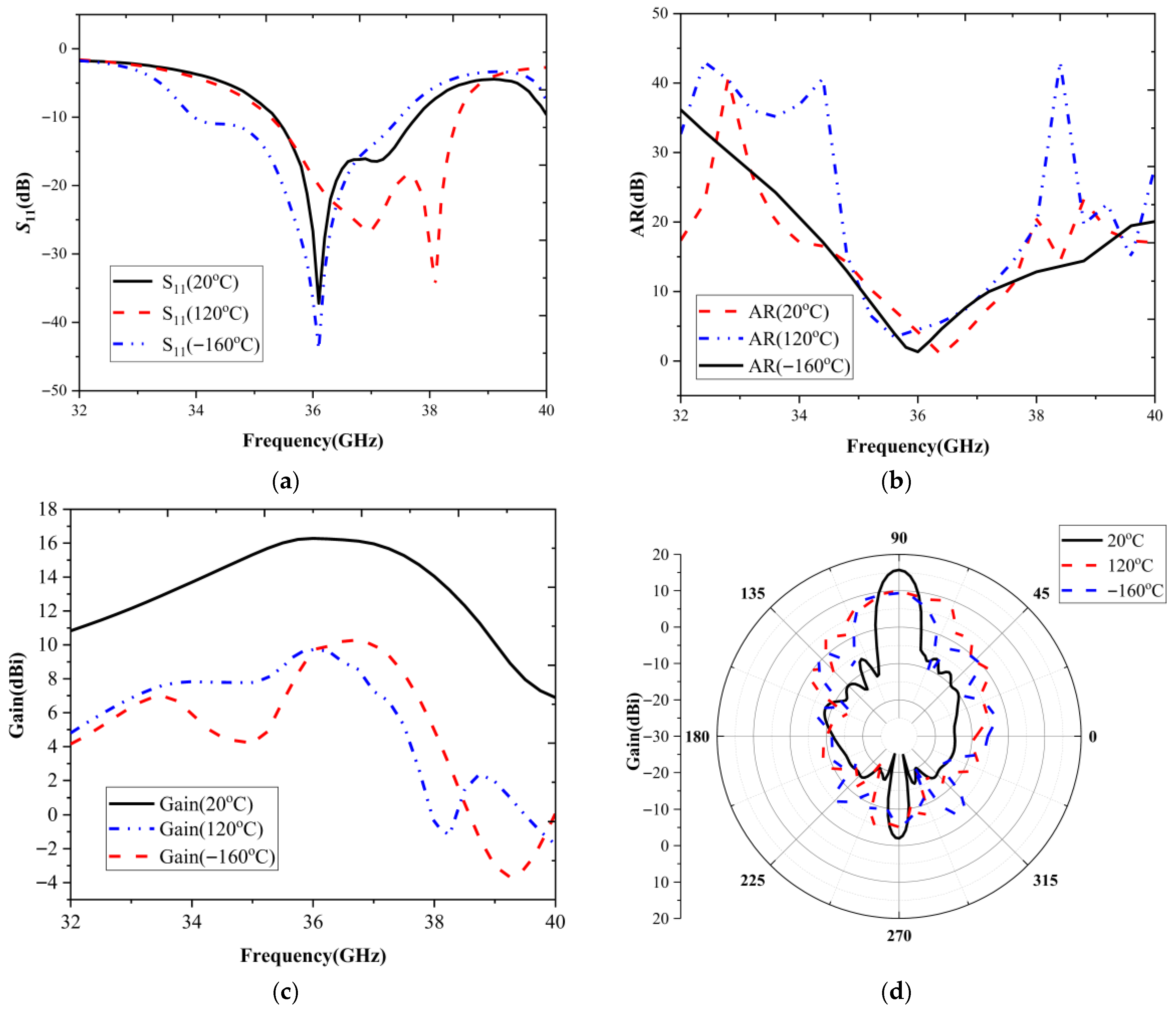
Thermal deformation of the array leads to degradation in its electrical performance. As shown in Figure 8a,b, both the resonant frequency and the AR shift towards the higher frequencies under the high-temperature conditions, whereas they shift towards lower frequencies under the low-temperature conditions. Furthermore, Figure 8c,d illustrate the variation of the gain with respect to frequency and angle θ. In the high-temperature environment, the antenna array gain decreases significantly, from 16.22 dBi to 9.82 dBi—a reduction of 6.40 dB. The half-power beamwidth at φ = 90° plane widens from 11.23° to 39.72°. The main lobe magnitude decreases, while the sidelobe level increases from −22.1 dB to −5.97 dB, resulting in the loss of a well-defined radiation pattern with main lobe and sidelobe structure. Under the low-temperature environment, the antenna gain also decreases markedly from 16.22 dBi to 9.78 dBi, corresponding to a decrease of 6.44 dB. The half-power beamwidth at φ = 90° plane increases from 11.23° to 29.46°. The main lobe magnitude is decreased, and the sidelobe level rises from −22.1 dB to −8.71 dB.
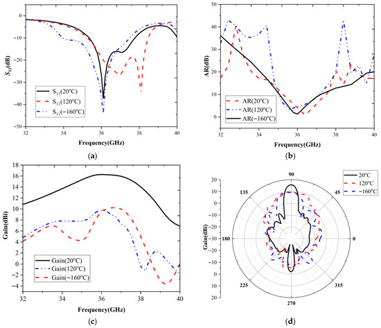
Figure 8.
Electrical parameters of the original array in different temperatures: (a) S11; (b) AR; (c) Gain; (d) Radiation patterns at φ = 90°.
Hence, if the antenna array works in a high or low temperature environment, it does not meet the requirement of SLL < −15 dB. The degradation indicates a reduced ability to suppress clutter and diminished anti-interference ability.
4. Optimization Design by Strain Compensation Method
Under extreme temperature conditions, antenna arrays are susceptible to thermal deformation, which is the primary reason for electrical performance degradation. Minimizing the deformation of the antenna array is crucial for maintaining performance stability. To address this issue, this paper proposes a strain compensation method to optimize the antenna array structure. Many slits are designed on the array ground plate with large-strain regions to mitigate thermal deformation under extreme temperature conditions in this method. A detailed introduction to the positions and sizes of the slits is presented below.
4.1. Slits Positions
The influence of slits positions on strain distribution within the array is systematically investigated. The slits are assumed to have consistent dimensions: 6.7 mm in length, 0.1 mm in width, and 0.035 mm in thickness. Strain distributions are analyzed using COMSOL simulation.
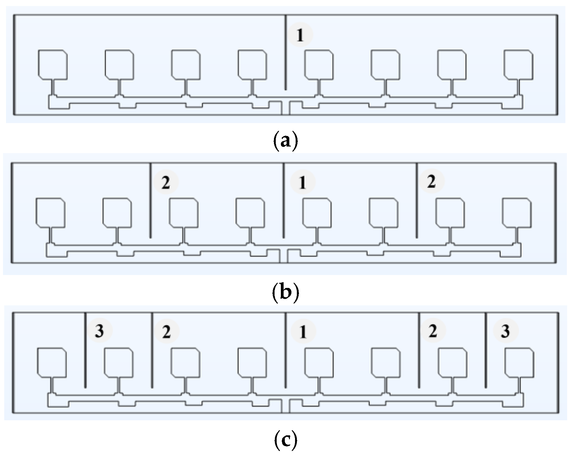
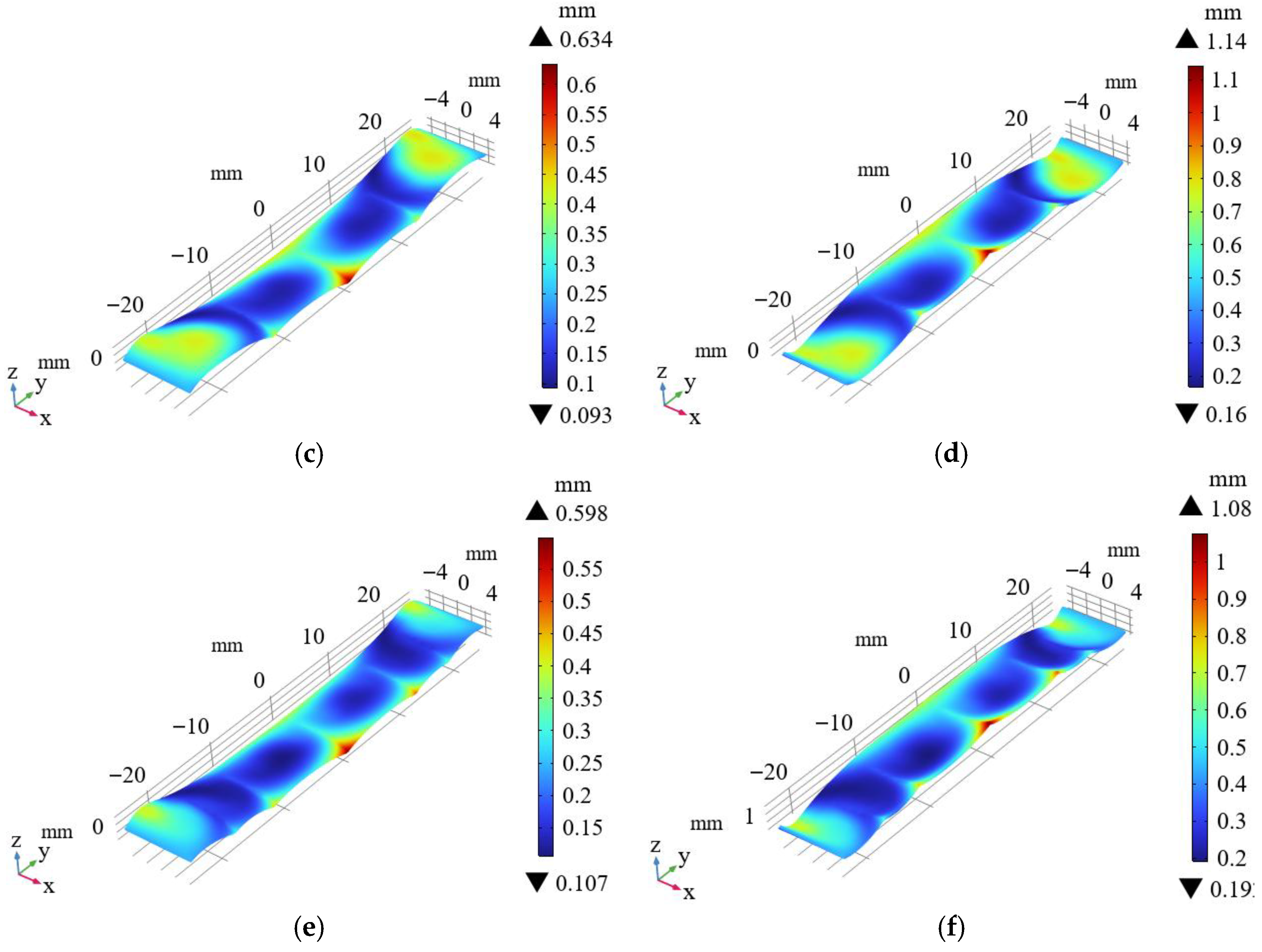
As shown in Figure 7, the maximum strain in the original array is located at the center. A slit is first introduced at position 1 as shown in Figure 9a. The resulting strain distributions under high and low temperature conditions are shown in Figure 10a,b, respectively. It can be observed that the slit can interrupt the continuous strain distribution, leading to a significant reduction in strain magnitude and the emergence of two new strain peaks on the left and right sides. Based on this principle—introducing slits in regions of maximum strain—a second set of slits is added at the new high-strain locations, as shown in Figure 9b. This process is repeated iteratively. Figure 9 illustrates the slit configurations at different stages, and Figure 10 presents the corresponding strain distributions. The final slit layout, determined by successively placing slits in areas of peak strain, is shown in Figure 9c. In the configuration with three sets of slits, the maximum strain is concentrated near the left and right ends of the array. Since the excitation current at these ends is relatively low, deformation in these regions has a diminished impact on radiation performance. Therefore, this configuration is expected to yield optimal antenna performance.
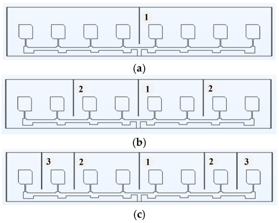
Figure 9.
Different slits positions: (a) One slit in position 1; (b) One slit in position 1 and a set of slits in position 2; (c) One slit in position 1, a set of slits in position 2 and a set of slits in position 3.
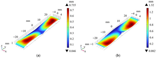
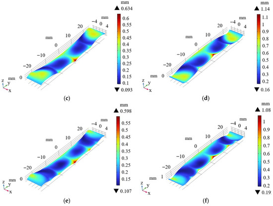
Figure 10.
Stain distributions of the array with different slits: (a) One slit with high-temperature; (b) One slit with low-temperature; (c) Two sets of slits with high-temperature; (d) Two sets of slits with low-temperature; (e) Three sets of slits with high-temperature; (f) Three sets of slits with low-temperature.
4.2. Slit Sizes
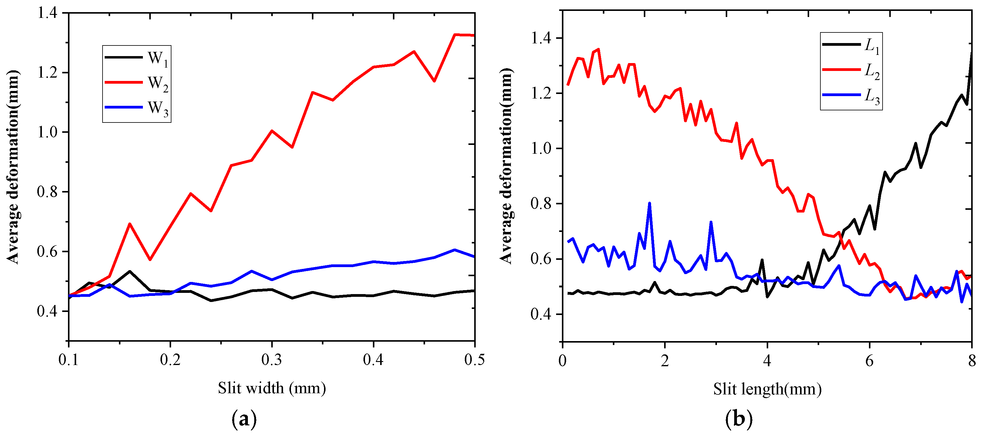
The positions of the slits are determined, and the next step is to optimize each slit size of the array. Figure 11 illustrates how the average deformation of the array varies with the width and length of the slits. As seen in Figure 11a, the average deformation increases with the width of Slit 2, while it shows negligible variation with the widths of Slit 1 and Slit 3. Therefore, the slit width should be made as small as possible to minimize thermal deformation under extreme temperatures. However, the precision of the manufacturing process can only reach 0.1 mm; thus, all slit widths have to be set to a width of 0.1 mm. Since the slits are etched on the copper ground plate, the depths of the slits are 0.035 mm, equal to the thickness of the copper layer. In addition, Figure 11b indicates that the average deformation increases with the length of Slit 1, decreases with the length of Slit 2, and remains largely unaffected by the length of Slit 3.

Figure 11.
Variation of the average deformation in the array: (a) Width; (b) Length.
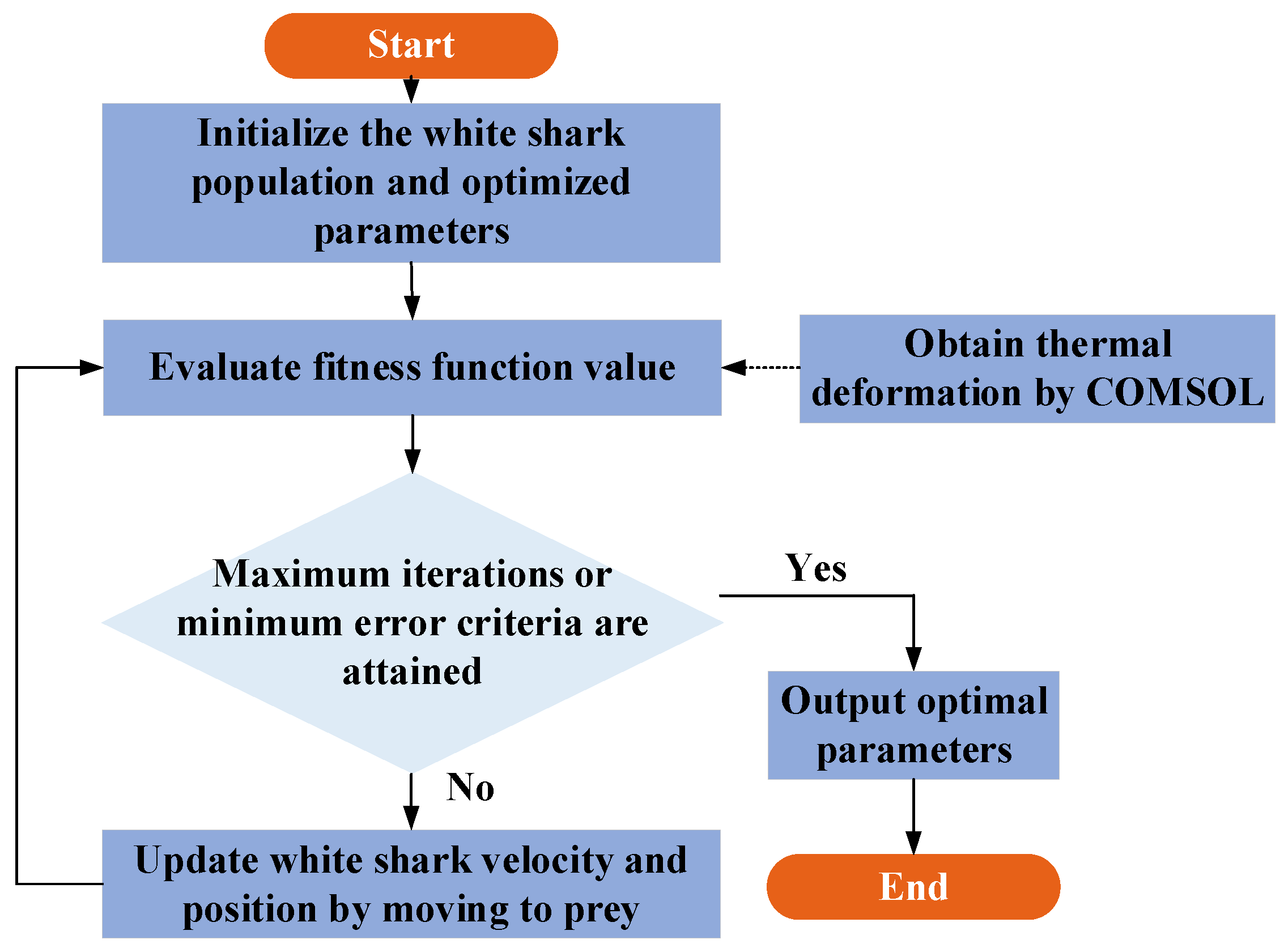
The WSO algorithm is used to optimize the lengths of the slits. The optimization process is outlined in the flowchart shown in Figure 12. The specific steps are as follows: (1) Initialize the population of white sharks and slit lengths; (2) Use MATLAB R2023a (Manufactured by Mathworks, Natick, MA, USA) to call COMSOL to simulate the array, thus obtaining the deformations. Calculate the fitness function value, defined as the average deformation of the array; (3) Check if the termination iteration condition is satisfied. If yes, output the optimal solution directly; If not, update the velocity and position of the white shark and return to Step 2. In addition, for the WSO algorithm, the population size and the maximum number of iterations are set to 15 and 30, respectively. When the maximum number of iterations is reached, return the best solution obtained so far.

Figure 12.
Flowchart of WSO Algorithm for optimizing the slit lengths.
The optimized lengths of the slits are listed in Table 4. The length of Slit 1 is L1 = 4.0 mm; that of Slit 2 is L2 = 6.7 mm, and that of Slit 3 is L3 = 7.8 mm, respectively.

Table 4.
Slit lengths of the optimized array with five slits.
4.3. Multi-Physics Fields Analysis of Optimized Array
The array exhibits enhanced thermal stability when deformation is reduced under extreme temperature conditions. Figure 13 and Figure 14 show the temperature and strain distributions of the optimized array under the high and low temperature conditions. It can be observed that the steady-state temperature distributions of the optimized and original arrays are similar. The strain in the optimized array is significantly lower than in the original design. Table 5 provides the maximum and average deformations of the optimized and original array under high and low temperature conditions. It can be seen that the optimized array exhibits significantly reduced deformation under extreme temperature conditions compared to the original design. Under the high-temperature condition, the maximum and average deformations were reduced by 95.61% and 97.49%, respectively. Under the low-temperature condition, the reductions were 95.33% and 97.39%, respectively. This indicates that the slits introduced on the ground plate have little effect on the temperature distribution but effectively suppress thermal deformation.

Figure 13.
Temperature distributions of the optimized array: (a) High-temperature; (b) Low-temperature.

Figure 14.
Strain distributions of the optimized array: (a) High temperature; (b) Low temperature.

Table 5.
Maximum and average deformation of the original and the optimized array.
Figure 15 shows the electrical parameters of the optimized array under the high, low, and normal temperature conditions. As can be observed, the S11, AR, Gain, and radiation patterns under extreme temperatures align closely with those under normal temperature. Due to the reduced thermal deformation, the optimized array exhibits significantly improved thermal stability compared to the original design. The S11, AR and Gain are the identical at 36 GHz under both high and low temperature conditions. A comparison of the gain between the proposed and original arrays is presented in Table 6. The maximum gain at 36 GHz increases by 65.17% under high temperature and 68.10% under low temperature.
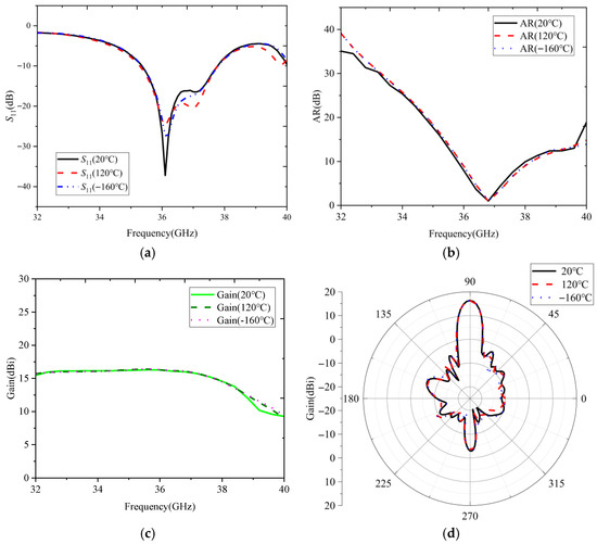
Figure 15.
Electrical performance parameters of the optimized array in different temperatures: (a) S11; (b) AR; (c) Gain; (d) Radiation patterns at φ = 90°.

Table 6.
Comparison of the gain between the proposed and original arrays (36 GHz).
5. Experimental Validation
To verify the effectiveness of the proposed method, a physical prototype of the antenna array is fabricated and measured. However, it is challenging to simulate a vacuum environment in an actual laboratory. Furthermore, standard antenna measurement systems are not designed to operate under extreme temperature conditions, making direct measurement in such an environment unfeasible. Therefore, the experimental validation is conducted in an air environment rather than under vacuum conditions. Critically, the marked difference in thermal propagation between air and vacuum results in a predictably higher equilibrium temperature under vacuum for the same input power. Consequently, these experimental results provide only an approximate validation of the simulated outcomes.
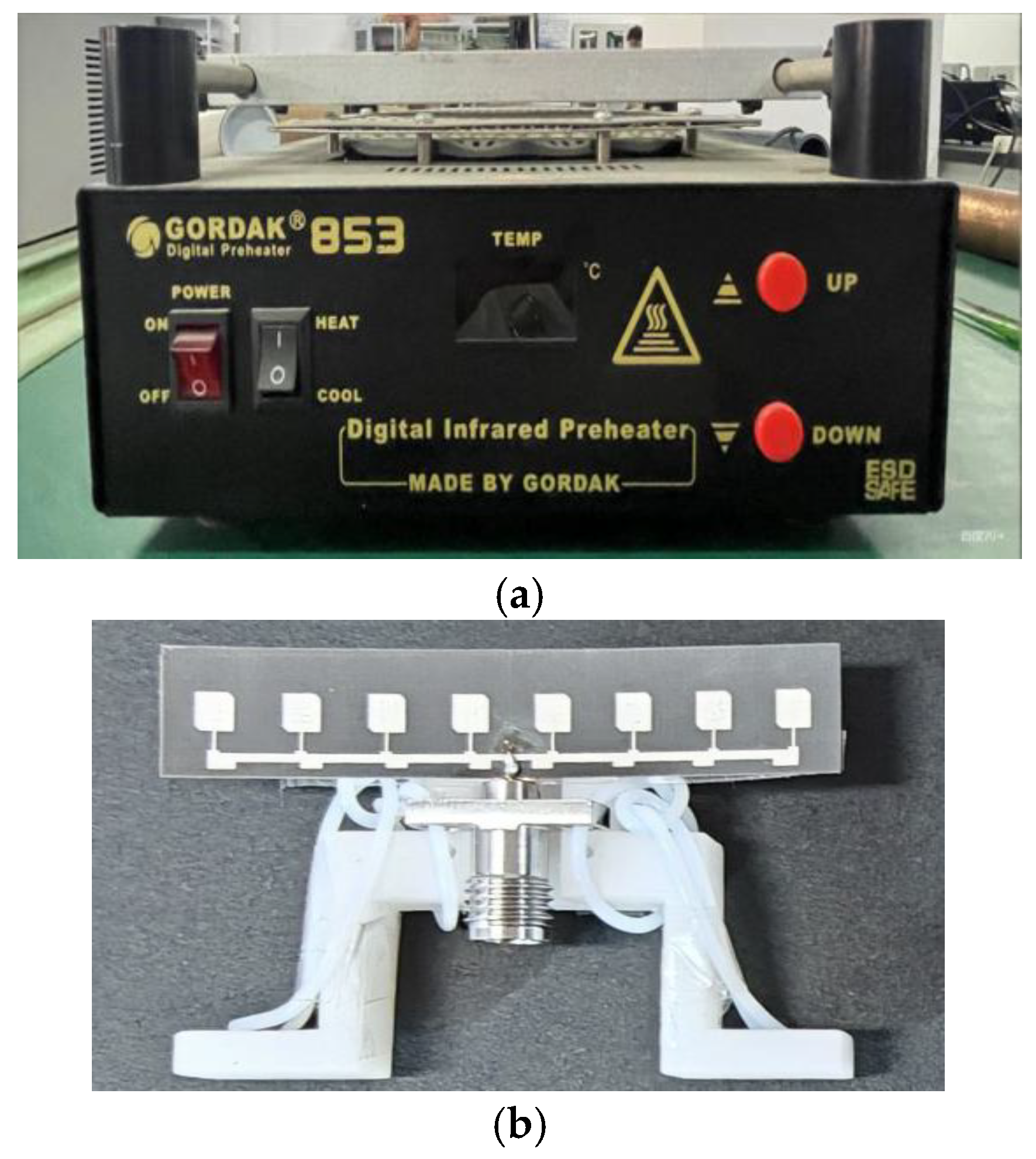
Taking the high temperature condition as an example, the electrical parameters of the fabricated array can be indirectly measured. The array is first heated to a steady state on a constant-temperature heating table, as shown in Figure 16a. An infrared thermometer is used to measure the temperature of the array. When the measured temperature remains unchanged within 10 min, the array is considered to have reached a steady-state temperature. The steady-state array is shown in Figure 16b. It is then quickly transferred to the pre-configured measurement platform illustrated in Figure 16c for electrical parameters measurement. Since both the temperature and deformation of the array change slowly, it can be assumed that they remain approximately constant for a short period after reaching steady state, allowing for valid measurements.

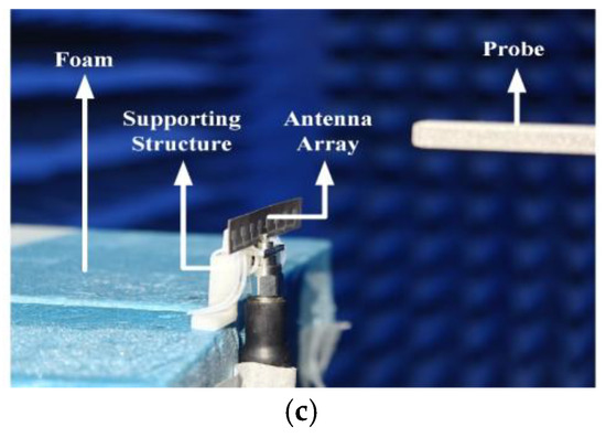
Figure 16.
Real experiment scene: (a) Constant temperature heating table; (b) Real array; (c) Real experiment.
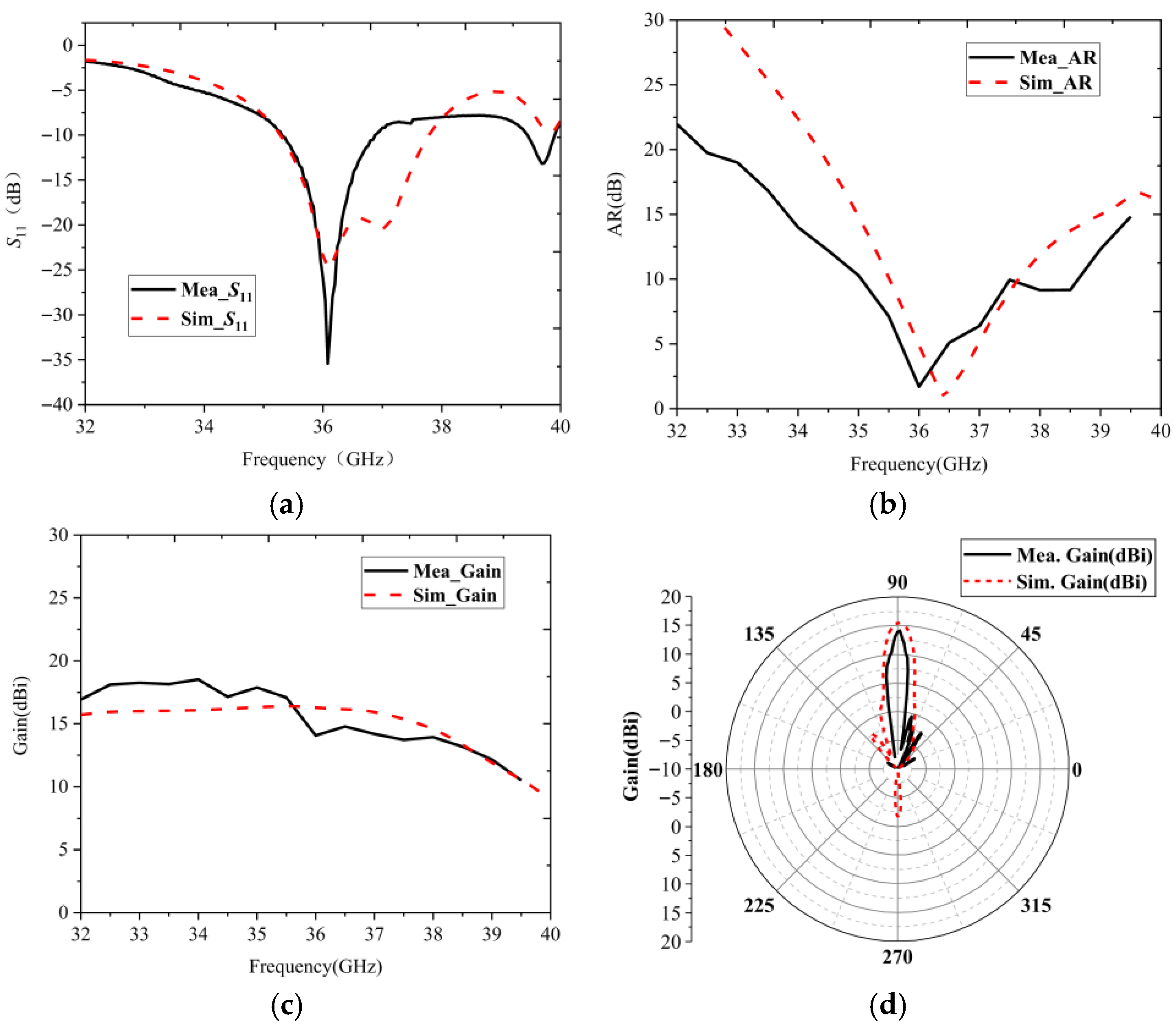
A vector network analyzer is employed to measure the S-parameters of the antenna array in its steady state. As shown in Figure 17a, the simulated and measured results are in good agreement. A near-field testing system is used to capture the near-field distribution, and the far-field radiation characteristics are subsequently derived through near-field and far-field transformations. The measured AR, gain, and radiation patterns are shown in Figure 17b,c,d, respectively. While the measured trends align with the simulations, certain deviations are observed. This can be attributed to the following factors: (1) deviations between the actual measurement environment and idealized simulation conditions; (2) limitations inherent to the measurement techniques; and (3) imperfections introduced during the manufacturing processes.
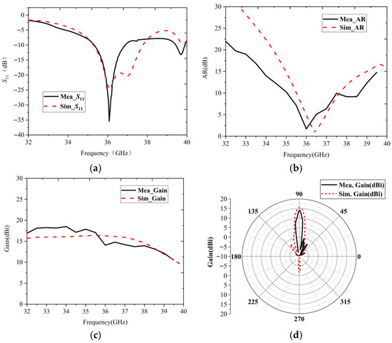
Figure 17.
Measurement and simulation results of the real array: (a) S11; (b) AR; (c) Gain; (d) Patterns at φ = 90°.
6. Conclusions
To ensure the reliable performance of spaceborne antenna arrays under extreme temperature conditions, this paper presents an optimized structural design method based on strain compensation. The method employs COMSOL software to analyze the thermal-structural-electromagnetic couplings behavior of the spaceborne microstrip arrays under extreme temperature conditions, mapping both the deformation and thermal-strain distribution. Based on the analysis, strategically designed slits are introduced in regions of high-strain concentration to redistribute strain and mitigate thermal deformation. This optimized configuration maintains superior electrical performance while significantly enhancing thermal stability. Simulation and measurement results collectively have verified the effectiveness of the proposed optimization design method. However, the significant difference in heat propagation between air and a vacuum environment means that the experimental results can only be used for approximate verification of the simulations. Importantly, the proposed method offers a novel solution for mitigating thermal-induced performance degradation in spaceborne antenna systems without requiring active thermal control.
Author Contributions
Conceptualization, K.F. and S.W.; methodology, K.H. and Q.X.; software, H.L. and H.W.; validation, K.H., H.L. and H.W.; formal analysis, K.F.; writing—K.F. All authors have read and agreed to the published version of the manuscript.
Funding
This work was funded by the National Key Research and Development Program of China (No. 2022YFA1604600), and funded by the Shaanxi Natural Science Basic Research Project of Shaanxi Science and Technology Office (No. 2023-JC-QN-0673), and funded by Key R&D Program of Shaanxi Province (No.2024GX-ZDCYL-05-04), and funded by the Shaanxi Province Innovation Capability Support Plan (No. 2024RS-CXTD-07).
Data Availability Statement
Data are contained within the article.
Conflicts of Interest
Author Kui Huang and Qi Xiao are employed by Beijing Institute of Spacecraft Environment Engineering. The remaining authors declare that the research was conducted in the absence of any commercial or financial relationships that could be construed as a potential conflict of interest.
References
- Capovilla, G.; Cestino, E.; Reyneri, L.M.; Romeo, G. Modular multifunctional composite structure for CubeSat applications: Preliminary design and structural analysis. Aerospace 2020, 7, 17. [Google Scholar] [CrossRef]
- Saeed, N.; Elzanaty, A.; Almorad, H.; Dahrouj, H.; Al-Naffouri, T.Y.; Alouini, M.S. CubeSat communications: Recent advances and future challenges. IEEE Commun. Surv. Tutor. 2020, 22, 1839–1862. [Google Scholar] [CrossRef]
- Cappelletti, C.; Robson, D. CubeSat missions and applications. In CubeSat Handbook; Elsevier: Amsterdam, The Netherlands, 2021; pp. 53–65. [Google Scholar]
- Constantine, A.B. Antenna Theory: Analysis and Design; John Wiley & Sons: Hoboken, NJ, USA, 2016. [Google Scholar]
- Chahat, N. CubeSat Antenna Design; Wiley: Hoboken, NJ, USA, 2021; pp. 233–253. [Google Scholar]
- Buttazzoni, G.; Comisso, M.; Cuttin, A.; Fragiacomo, M.; Vescovo, R.; Gatti, R.V. Reconfigurable phased antenna array for extending CubeSat operations to Ka-band: Design and feasibility. Acta Astronaut. 2017, 137, 114–121. [Google Scholar] [CrossRef]
- Sundu, H.; Döner, N. Detailed thermal design and control of an observation satellite in low Earth orbit. Eur. Mech. Sci. 2020, 4, 171–178. [Google Scholar] [CrossRef]
- Tsai, J.R. Overview of satellite thermal analytical model. J. Spacecr. Rocket. 2004, 41, 120–125. [Google Scholar] [CrossRef]
- Hayashi, I.; Higuchi, R.; Yokozeki, T.; Aoki, T. Analytical study on the thermal deformation of ultralight phased array antenna. Acta Astronaut. 2021, 188, 531–544. [Google Scholar] [CrossRef]
- Wresnik, J.; Haas, R.; Boehm, J.; Schuh, H. Modeling thermal deformation of VLBI antennas with a new temperature model. J. Geod. 2007, 81, 423–431. [Google Scholar] [CrossRef]
- Liu, H.; Wang, W.; Tang, D.; Zhang, L.; Wang, Y.; Miao, E. Thermal deformation modeling for phased array antenna compensation control. Sensors 2022, 22, 2325. [Google Scholar] [CrossRef]
- Yoon, H.S.; Washington, G. An optimal method of shape control for deformable structures with an application to a mechanically reconfigurable reflector antenna. Smart Mater. Struct. 2010, 19, 105004. [Google Scholar] [CrossRef]
- Yang, G.; Tang, A.; Yuan, Z.; Yang, Z.; Li, S.; Li, Y. Surface shape stability design of mesh reflector antennas considering space thermal effects. IEEE Access 2020, 8, 89071–89083. [Google Scholar] [CrossRef]
- Shi, Z.; Zhou, Q.; Zhu, H.; Yang, W.; Meng, N. Thermal-dynamic coupling analysis of space truss antennas in actual space thermal environment. Eng. Struct. 2024, 298, 117020. [Google Scholar] [CrossRef]
- Xu, P.; Wang, Y.; Xu, X.; Wang, L.; Wang, Z.; Yu, K.; Wu, W.; Wang, M.; Leng, G.; Ge, D.; et al. Structural-electromagnetic-thermal coupling technology for active phased array antenna. Int. J. Antennas Propag. 2023, 2023, 2843443. [Google Scholar] [CrossRef]
- Feng, S.; Sun, Q.; Wu, Y.; Han, X.; Li, Z.; Angel Sotelo, M. Stochastic thermal–structural–electromagnetic coupling analysis of phased arrays with random material parameters. IEEE Trans. Antennas Propag. 2023, 71, 8030–8039. [Google Scholar] [CrossRef]
- Xu, W.; Zhu, H.; Zhang, X. Thermal–mechanical coupling performances and parameters sensitivity analyses of a deployable Astromesh antenna under different heat radiations. Appl. Therm. Eng. 2025, 259, 124732. [Google Scholar] [CrossRef]
- Nie, R.; He, B.; Yan, S.; Ma, X. Optimization design method for mesh reflector antennas considering the truss deformation and thermal effects. Eng. Struct. 2020, 208, 110253. [Google Scholar] [CrossRef]
- Xu, W.; Zhu, H.; Li, J. On-orbit thermal-mechanical coupling performance analysis of a deployed hoop-column antenna. Thin-Walled Struct. 2025, 214, 113312. [Google Scholar] [CrossRef]
- Dong, T.; Yuan, S.; Huang, T. Real-time shape sensing of large-scale honeycomb antennas with a displacement-gradient-based variable-size inverse finite element method. Compos. Struct. 2024, 344, 118320. [Google Scholar] [CrossRef]
- Fenf, S.; Wang, H.; Li, Z. An enhanced computational approach for multi-physics coupling analysis of active phased array antenna. Eng. Anal. Bound. Elem. 2024, 167, 105892. [Google Scholar]
- Jin, L.; Zhang, F.; Tian, D.; Wang, Q.; Cao, Q. Thermal-structural analysis of the support structure for a modular space deployable antenna. Int. J. Aerosp. Eng. 2022, 2022, 2164485. [Google Scholar] [CrossRef]
- Nösekabel, E.-H.; Ernst, T.; Haefker, W. Measurement of the thermal deformation of a highly stable antenna with pulse ESPI. Proc. SPIE 2007, 6616, 66162X. [Google Scholar]
- Yuan, S.; Sun, G.; Yu, K.; Zhou, K.; Cheng, Z.; Zhu, L. In-orbit thermal deformation monitoring for composite laminated structures of remote sensing satellites using temperature self-decoupling fiber optical system and inverse finite element method. Appl. Phys. B 2024, 130, 45. [Google Scholar] [CrossRef]
- Ma, K.; Huang, G.; Meng, J. Thermal deformation measurement of the surface shape of a satellite antenna using high-accuracy close-range photogrammetry. Sensors 2024, 24, 4722. [Google Scholar] [CrossRef] [PubMed]
- Simone, M.; Fanti, A.; Valente, G.; Montisci, G.; Ghiani, R.; Mazzarella, G. Optimized design and multiphysics analysis of a KA-band stacked antenna for CUBESAT applications. IEEE J. Multiscale Multiphys. Comput. Tech. 2021, 6, 143–157. [Google Scholar] [CrossRef]
- Wang, P.; Wang, F.; Shi, T.; Wang, B. Thermal distortion compensation of a high precision umbrella antenna. J. Phys. Conf. Ser. 2017, 916, 012051. [Google Scholar] [CrossRef]
- Wei, X.; Miao, E.; Wang, W.; Liu, H. Real-time thermal deformation compensation method for active phased array antenna panels. Precis. Eng. 2019, 60, 121–129. [Google Scholar] [CrossRef]
- Yu, H.; Wang, H.; Wang, X.; Lei, H.; Guo, X. The metamaterial with high thermal-mechanical stability and the practical application as the microwave antenna: Mechanical designs, theoretical predictions, and experimental demonstrations. Extrem. Mech. Lett. 2024, 69, 1002166. [Google Scholar] [CrossRef]
- Lu, G.Y.; Zhou, J.Y.; Cai, G.P.; Fang, G.Q.; Lv, L.L.; Peng, F.J. Studies of thermal deformation and shape control of a space planar phased array antenna. Aerosp. Sci. Technol. 2019, 93, 105311. [Google Scholar] [CrossRef]
- Jin, C.; Liu, X.; Cai, G.; Sun, J.; Zhu, D. Thermal deformation analysis and shape control of a novel large-scale two-dimensional planar phased array antenna. Astrodynamics 2025, 9, 583–604. [Google Scholar] [CrossRef]
- Braik, M.; Hammouri, A.; Atwan, J.; Al-Betar, M.A.; Awadallah, M.A. White Shark Optimizer: A novel bio-inspired meta-heuristic algorithm for global optimization problems. Knowl.-Based Syst. 2022, 243, 108457. [Google Scholar] [CrossRef]
Disclaimer/Publisher’s Note: The statements, opinions and data contained in all publications are solely those of the individual author(s) and contributor(s) and not of MDPI and/or the editor(s). MDPI and/or the editor(s) disclaim responsibility for any injury to people or property resulting from any ideas, methods, instructions or products referred to in the content. |
© 2025 by the authors. Licensee MDPI, Basel, Switzerland. This article is an open access article distributed under the terms and conditions of the Creative Commons Attribution (CC BY) license (https://creativecommons.org/licenses/by/4.0/).


