1. Introduction
Field-Programmable Gate Arrays (FPGAs) have emerged as a critical enabler for achieving application performance in a post-Moore’s Law era [
1]. FPGAs provide inherent flexibility, enabling rapid prototyping, iterative design, and the ability to reconfigure the hardware after manufacturing. This flexibility is especially valuable in fields such as telecommunications, automotive systems, aerospace, signal processing, and embedded systems, where design requirements often may require changes.
The reconfigurable nature of FPGAs also plays a crucial role in the domain of network infrastructure, where they are used in software-defined networking, network function virtualization, and edge computing. FPGAs provide the necessary programmability and adaptability to handle evolving network protocols and traffic patterns, enhancing performance, scalability, security in modern network architectures, and evolving deep learning and machine learning algorithms as well [
2].
The parallel processing capabilities of FPGAs with their ability to implement complex algorithms and customized hardware accelerators have made them indispensable in high-performance computing applications. From machine learning and artificial intelligence to data analytics and cryptography, FPGAs have demonstrated remarkable performance, energy efficiency, and real-time processing capabilities, enabling the acceleration of computationally intensive tasks [
2,
3,
4].
Moreover, FPGAs have found extensive use in the development of digital system prototypes, allowing designers to make pre-silicon validation in hardware before manufacturing expensive Application-Specific Integrated Circuits (ASICs). FPGAs enable faster time to market by facilitating rapid prototyping, system integration, and software-defined hardware platforms [
5]. This flexibility also makes FPGAs an ideal choice for research and development projects, where frequent design iterations, experimentation, and customization are required.
The RTL-to-GDSII workflow, which converts a Register Transfer Level (RTL) description of a digital circuit into a finalized Graphic Data System II (GDSII) layout, is fundamental in FPGA design. It encompasses several key stages—synthesis, floorplanning, placement, routing, and verification—that together lead to the physical implementation of the circuit [
6]. Despite the growing relevance of FPGAs and the availability of open-source toolchains such as OpenLane and OpenFPGA, there is no detailed methodology in the literature that demonstrates how to create, validate, and fabricate a custom embedded FPGA at the layout level.
Prior work on FPGA fabrics has made notable strides but still leaves gaps in the reproducibility and transparency of the physical design flow. Dao et al. [
7] couple FABulous to an RISC-V CPU in a 180 nm commercial process using a proprietary PDK and Synopsys/Cadence toolchains; OpenFPGA [
8] reports architectural resources and area metrics; and Moser et al. [
9] tightly integrate FABulous with OpenLane 2 to automate the assembly of homogeneous fabrics via automatic macro placement. However, these studies do not comprehensively document layout configuration (e.g., floorplanning strategy, routing/clocking options, corner selection, runtime and peak-memory settings), which hinders faithful reproduction—especially for newcomers to open-source flows.
Notably, among these works, only [
9] employs an open-source PDK; the others rely on proprietary PDKs typically restricted by non-disclosure agreements (NDAs), which further limits transparency and reusability. Moreover, these studies omit detailed documentation of the physical design phase, a gap that significantly undermines reproducibility—especially for newcomers who depend on open-source flows.
The motivation for this research arises from the growing importance of FPGAs; their flexibility makes them indispensable in a post-Moore’s Law era, where rapid design iterations and hardware adaptability are essential. Despite the availability of powerful open-source tools like OpenFPGA and OpenLane, the literature still lacks a standardized and validated methodology that connects architectural description with physical implementation, progressing seamlessly from RTL design to a fabricable GDSII layout. This absence of a comprehensive workflow hinders researchers and practitioners who aim to develop custom embedded FPGA architectures beyond functional simulation.
The existing problem is further complicated by the inherent complexity of the RTL-to-GDSII flow, which requires coordinating multiple interdependent stages such as synthesis, floorplanning, placement, routing, and verification. Current resources are fragmented and tool-specific, offering only partial guidance that fails to guarantee reproducibility or scalability. Designers are often left to navigate compatibility issues, steep learning curves, and unpredictable outcomes, making the process inefficient and error-prone. This work addresses these challenges by proposing an integrated, reproducible open-source methodology that leverages OpenFPGA for architectural flexibility and OpenLane for automated physical design, thereby bridging the gap between theory and fabrication.
The decision to utilize OpenFPGA alongside other tools is driven by its comprehensive coverage of several critical metrics. OpenFPGA offers features such as being open-source, supporting an architecture description language, netlist generation, bitstream generation, testbench generation, and Synopsys Design Constraint (SDC) file generation.
Table 1 presents a comparison of these features with other tools [
10].
The research problem addressed in this work is the absence of a documented and validated methodology for designing custom embedded FPGA architectures that progress beyond functional RTL simulation to a fully verified GDSII layout ready for fabrication. Without such a workflow, researchers and engineers face fragmented, tool-specific documentation that does not demonstrate scalability or reproducibility.
Currently, there are only three open-source, fabricable Process Design Kits (PDK) with multiple layers: SKY130 [
14], GF180MCU [
15], and IHP-130 [
16]. All of these have been successfully manufactured using the OpenROAD EDA tool. However, OpenROAD requires a step-by-step development approach. For this reason, the decision was made to use OpenLane, which automates the RTL-to-GDSII process by integrating OpenROAD with a series of custom scripts. By using OpenLane, the development time required for physical design is significantly reduced, streamlining the entire process.
The objective of this research is to close this methodological gap by proposing and validating a reproducible open-source RTL-to-GDSII workflow for embedded FPGA architectures. Unlike existing documentation, this study frames the process as a research problem—evaluating its feasibility, limitations, and opportunities for scalability.
Furthermore, this research addresses the absence of a standardized methodology for the physical design of custom embedded FPGA architectures. By leveraging open-source toolchains, the proposed workflow demonstrates how architectural description, RTL design, and physical implementation can be seamlessly integrated into a reproducible RTL-to-GDSII process. In doing so, this study highlights not only the practical feasibility of open-source approaches for FPGA layout design but also their broader role in enabling collaboration, innovation, and accessibility in the semiconductor research community.
The main contributions of this work are as follows:
Identification and formalization of the lack of a comprehensive methodology for embedded FPGA layout design using open-source tools.
Presentation and validation of a complete RTL-to-GDSII workflow that integrates OpenFPGA and OpenLane, demonstrated on a non-trivial embedded FPGA fabric.
Provision of performance, area, and design insights that highlight both the potential and the limitations of open-source toolchains for advancing custom FPGA architectures.
The remainder of this paper is organized as follows.
Section 2 introduces the analysis of development tools, focusing on OpenLane as the open-source RTL-to-GDSII flow and OpenFPGA as the framework for architectural customization and bitstream generation.
Section 3 details the proposed workflow, beginning with the creation of custom FPGA architectures in OpenFPGA, followed by pin planning, full testbench verification, and the transfer of RTL descriptions into OpenLane for physical implementation.
Section 4 presents a case study in which a semi-customized FPGA fabric is designed, verified, and implemented, illustrating the practicality of the methodology from RTL to GDSII.
Section 5 reports experimental results, including area, frequency, power consumption of hardened macros, core layout integration, and gate-level simulation outcomes validating the functional correctness of the design.
Section 6 provides a discussion of the results, highlighting the strengths and limitations of the proposed methodology, comparing it to prior work, and outlining potential improvements and future research directions. Finally,
Section 7 concludes the paper, emphasizing the feasibility of open-source tools for reproducible FPGA layout design, their educational and research impact, and their potential to democratize hardware innovation.
3. Analysis of Workflow
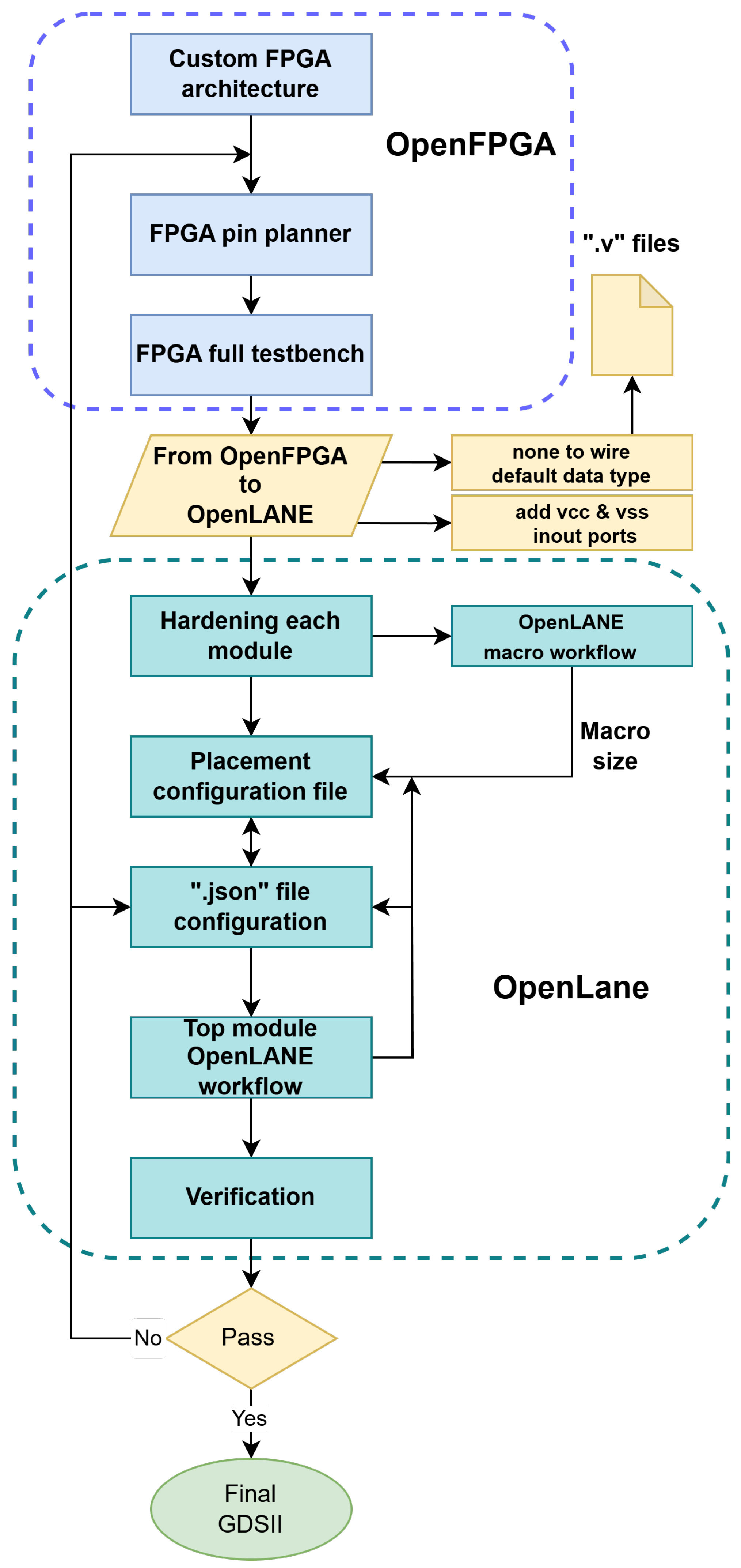
The RTL-to-GDSII workflow is a fundamental process in FPGA development by transforming a high-level RTL description into a final GDSII file ready for manufacturing. This workflow involves several crucial steps, starting with the creation of the FPGA architecture using OpenFPGA.
To ensure a successful GDSII generation, an additional step is necessary during the FPGA architecture creation, which involves the creation of the FPGA pin planner. The pin planner plays a crucial role in defining the placement and routing of input and output pins within the FPGA, ensuring proper connectivity and functionality. It allows designers to strategically position the pins to optimize signal integrity and minimize potential timing and routing issues.
After defining the architecture and pin planner, the FPGA undergoes a full simulation testbench that verifies behavior under multiple input scenarios, allowing early detection and correction of design errors.
The Verilog files are then exported to OpenLane, where minor edits improve compatibility: defaulting signals to wire and adding vcc/vss ports for a stable Power Delivery Network (PDN). Each main module proceeds through the RTL-to-GDSII flow, beginning with configuration files that set timing, power, and placement constraints to meet design goals.
Following the placement stage, the core configuration file, containing various design parameters, includes configuring timing constraints, power targets, and other performance criteria. A final gate-level simulation validates timing and functionality, exposing issues with power, delay, or signal integrity before fabrication.
In summary, the RTL-to-GDSII workflow for FPGAs is a multi-step process that involves various tools and methodologies. Starting with the creation of the FPGA architecture using OpenFPGA and the pin planner, followed by the full simulation testbench and Verilog file modifications, then in OpenLane, each main module undergoes the RTL-to-GDSII workflow. Creating the placement configuration file and performing gate-level simulation are vital stages in ensuring a successful FPGA design that meets all required specifications and design constraints.
Figure 3 illustrates the comprehensive workflow followed to obtain a successful GDSII file for an FPGA design.
3.1. Analysis of Custom FPGA Architecture Generation with OpenFPGA
To create an FPGA architecture with OpenFPGA, you can follow the steps outlined in the OpenFPGA documentation [
23]. The creation of an FPGA architecture using OpenFPGA can be approached in three different categories, each offering varying levels of customization.
In the fully customized category, users have complete control over the FPGA design by defining every module using the XML file format. This approach allows for detailed customization of the structure, functionality, and physical characteristics of the FPGA. The XML file serves as a powerful tool for specifying the hierarchical composition of the architecture, enabling the creation of complex designs from simpler building blocks. Users can define custom circuit models, interconnect networks, and timing characteristics, tailoring the FPGA architecture to their specific requirements. An example of this customization is shown in
Figure 2, which displays the XML description of the configurable logic blocks (CLB) and Look-Up Table (LUT) used in the architecture.
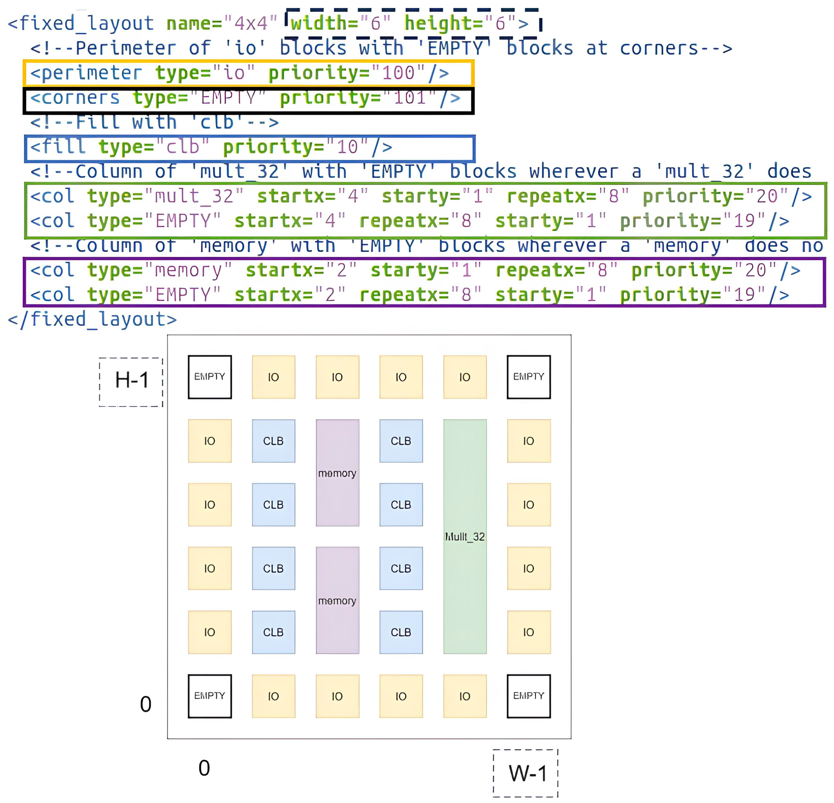
The semi-customized approach involves parameterization features, where users can modify design parameters to adapt the FPGA architecture to specific requirements. Parameters such as the number of CLBs, memory blocks, Digital Signal Processor (DSPs) blocks, inputs and outputs per I/O block, and other general parameters can be easily adjusted. By utilizing the architecture modeling language and the XML file format, designers have the flexibility to precisely tailor their FPGA architectures according to application needs, performance objectives, and design constraints.
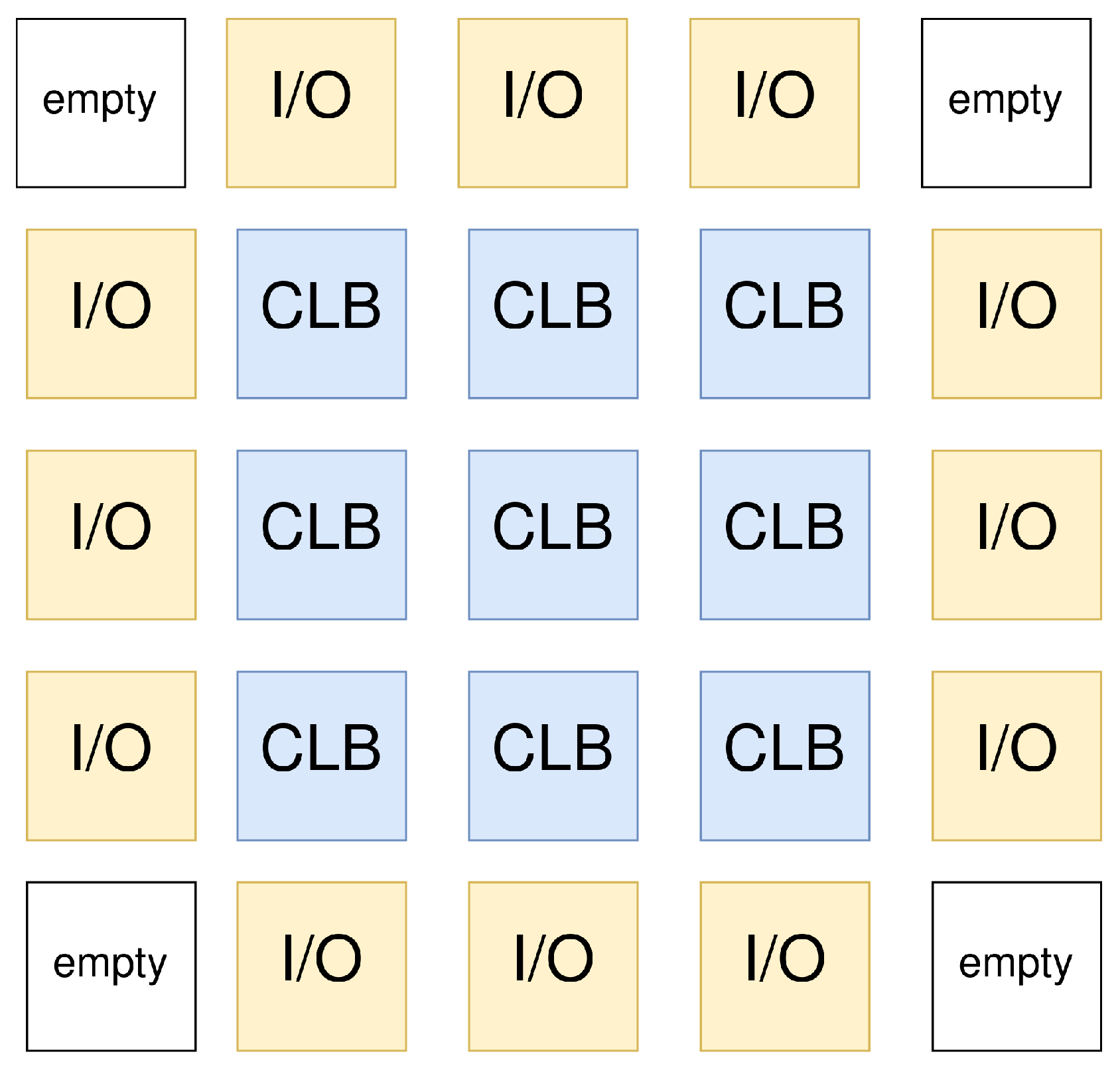
Figure 4 provides a visual representation of the semi-customized process. The figure uses color coding to distinguish different components and their code modification: gray indicates the number of blocks along the height (H) and width (W), yellow highlights the IO ports, black represents empty blocks reserved for routing, blue denotes the CLBs, green illustrates the DSP blocks, and purple identifies the memory blocks.
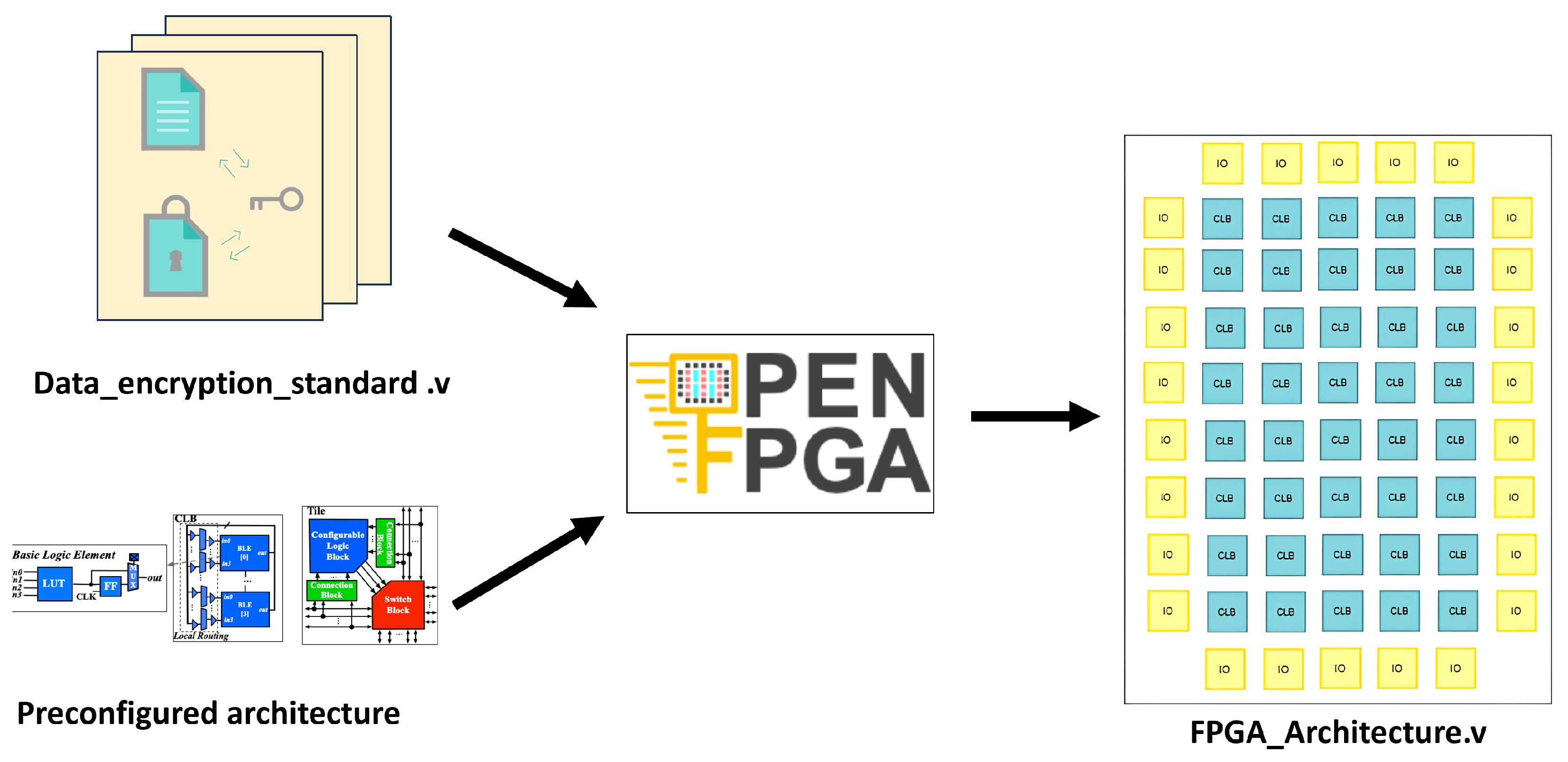
In the automatic category, a general FPGA architecture is chosen with default characteristics equal to the semi-customized approach. These characteristics include the type of LUT, number of inputs per LUT, number of LUTs per CLB, usage of adder blocks, DSP blocks, memory blocks, and configuration protocol. OpenFPGA then automatically generates the minimum necessary blocks to execute these designs. This approach provides a convenient and efficient way to create FPGA architectures. The level of automation involved in this approach can be visualized in
Figure 5.
By offering these three categories of customization, OpenFPGA empowers designers to create FPGA architectures that range from fully customized to automatic, catering to different levels of expertise, design requirements, and time constraints.
3.2. Analysis of Pin Planning for FPGA Connectivity in OpenFPGA
In FPGA design, a crucial parameter for precise input and output assignment is the pin planner. It enables the designer to assign specific pins on the FPGA for their design’s inputs and outputs, preventing random assignment. OpenFPGA requires three essential files to create an effective pin planner.
The first file is the openfpga_io_map_file, which is an XML file containing the coordinates of each I/O pin throughout the FPGA. It specifies the location of each pin using a basic structure like io_pad="gfpga_pad_GPIO_PAD[168]"x="0"y="1"z="0". Here, gfpga_pad_GPIO_PAD[168] represents the input name and bit, while the coordinates (x and y) indicate the tile’s position. The “z” parameter indicates the number of inputs/outputs in IO blocks.
The second file is the fpga_pin_table, which is a CSV file. It contains essential parameters such as orientation, port name, mapped pin name, and type. The structure of this file includes fields like orientation, row, col, pin_num_in_cell, port_name, mapped_pin, GPIO_type, Associated Clock, and Clock Edge. For example, a line in the file may look like TOP,,,,gfpga_pad_GPIO_PAD[0],pad_fpga_io[0],out,,.
The third file is the Pin Constraints File (PCF) called fpga_pcf. This file establishes the pin binding between the implementation and the FPGA fabric, specifying the connections between specific pins and components in the design.
By utilizing these files, the pin planner in OpenFPGA allows designers to precisely assign and control the input and output pins of their FPGA designs, ensuring proper connectivity and functionality.
3.3. Analysis of Full Testbench for Functional Verification
OpenFPGA employs two types of testbenches: the configuration phase and the operating phase. In the configuration phase, the bitstream is loaded into the FPGA. This phase ensures the correct configuration and functionality of the FPGA. In the operating phase, random input vectors are automatically generated to drive the Devices Under Test (DUTs) within the FPGA. This phase allows users to validate the overall functionality and performance of the FPGA, including its customized circuits and the programmed fabric.
When both phases are utilized together, it is referred to as a full testbench. By using the full testbench approach, users can thoroughly test and validate both the configuration circuits and the programming fabric of the FPGA, ensuring the correctness and reliability of their designs.
3.4. Analysis of RTL Transfer from OpenFPGA to OpenLane
As mentioned, when working with OpenFPGA, certain modifications need to be made to the FPGA Verilog file. By default, OpenFPGA generates a hierarchy file that contains information about the hierarchy of the FPGA. The main modules that need to be modified are those following the FPGA_top module. By default, the main modules include IO blocks, CLBs, switching blocks, and connection blocks. The specific type and quantity of these modules will depend on the chosen FPGA architecture and its characteristics.
The modifications in the Verilog files’ design are required at both the macro level (instances) and core level (top module). To incorporate the necessary power grid functionality, the ifdef USE_POWER_PINS parameter is added, usually called vcc and vss. Within this ifdef statement, the <power_pin> and <ground_pin> are included. This ensures that the power and ground connections are properly defined within the RTL code, enabling effective power distribution within the macro and core designs.
Another configuration to avoid syntax or routing errors with Yosys is to use the wire data type as the default type. By setting wire as the default data type, it ensures that all signals are explicitly defined as wires unless specified otherwise. This helps to prevent any unintended misinterpretation of signal types during synthesis and reduces the chances of potential errors. By following this configuration, it promotes clarity and accuracy in the FPGA design, contributing to a smoother synthesis and routing process. Finally, after making these changes to the Verilog files, they need to be exported to the OpenLane project.
3.5. Analysis of Macro Hardening in the RTL-to-GDSII Process
In order to obtain the GDSII file for each main module of the FPGA, a systematic process is followed within OpenLane. First, an OpenLane project is created for each module, with the number of modules depending on the specific FPGA architecture. Each module is then subjected to the RTL-to-GDSII workflow using OpenLane, treating them as individual macros. It is essential to ensure that each module adheres to the required basic configuration parameters, which are detailed in [
19]. These basic parameters are
DESIGN_NAME,
VERILOG_FILES,
CLOCK_PORT,
CLOCK_PERIOD,
FP_SIZING,
DIE_AREA,
FP_CORE_UTIL,
FP_PDN_MULTILAYER,
RT_MAX_LAYER,
VDD_NETS, and
GND_NETS.
To ensure the proper hardening of each module within the FPGA, it is essential to configure additional key parameters accurately. The specific parameters required depend on the macro module and the overall FPGA architecture. These parameters play a significant role in optimizing the performance and functionality of the FPGA design. Here are the key parameters and their significance:
GPL_CELL_PADDING: This parameter determines the spacing between cells in the placement process. It helps in avoiding any potential violations or timing issues caused by cell proximity.
FP_PDN_VPITCH, FP_PDN_HPITCH, and FP_PDN_VOFFSET: These parameters are associated with the PDN of the FPGA. They define the vertical and horizontal pitch, as well as the vertical offset, for the PDN grid.
DIODE_INSERTION_STRATEGY: This parameter controls the insertion strategy for diodes in the FPGA design. Diodes are commonly used to improve the reliability and robustness of the circuitry. Selecting an appropriate insertion strategy helps in achieving optimal diode placement for enhanced performance.
SYNTH_READ_BLACKBOX_LIB: When set to true, it indicates that the design utilizes standard cells, and the synthesis tool should consider them during the synthesis process.
PL_TARGET_DENSITY, PL_RESIZER_DESIGN_OPTIMIZATIONS, and PL_RESIZER_TIMING_OPTIMIZATIONS: These parameters are related to the placement process of the FPGA. They control the target density of the design and enable design optimizations at the placement stage to enhance performance and meet timing requirements.
RUN_CTS: This parameter determines whether to perform CTS during the FPGA synthesis process. CTS is essential for proper clock distribution and minimizing clock skew in the design.
GLB_RESIZER_TIMING_OPTIMIZATIONS, GRT_ADJUSTMENT: These parameters are associated with global routing in the FPGA design. They enable timing optimizations and adjustments during the global routing stage to meet critical timing constraints.
By understanding and appropriately configuring these parameters based on the OpenLane documentation, designers can effectively harden each module of the FPGA, ensuring optimal performance, timing, and reliability.
3.6. Analysis of Placement Configuration for Macro Integration
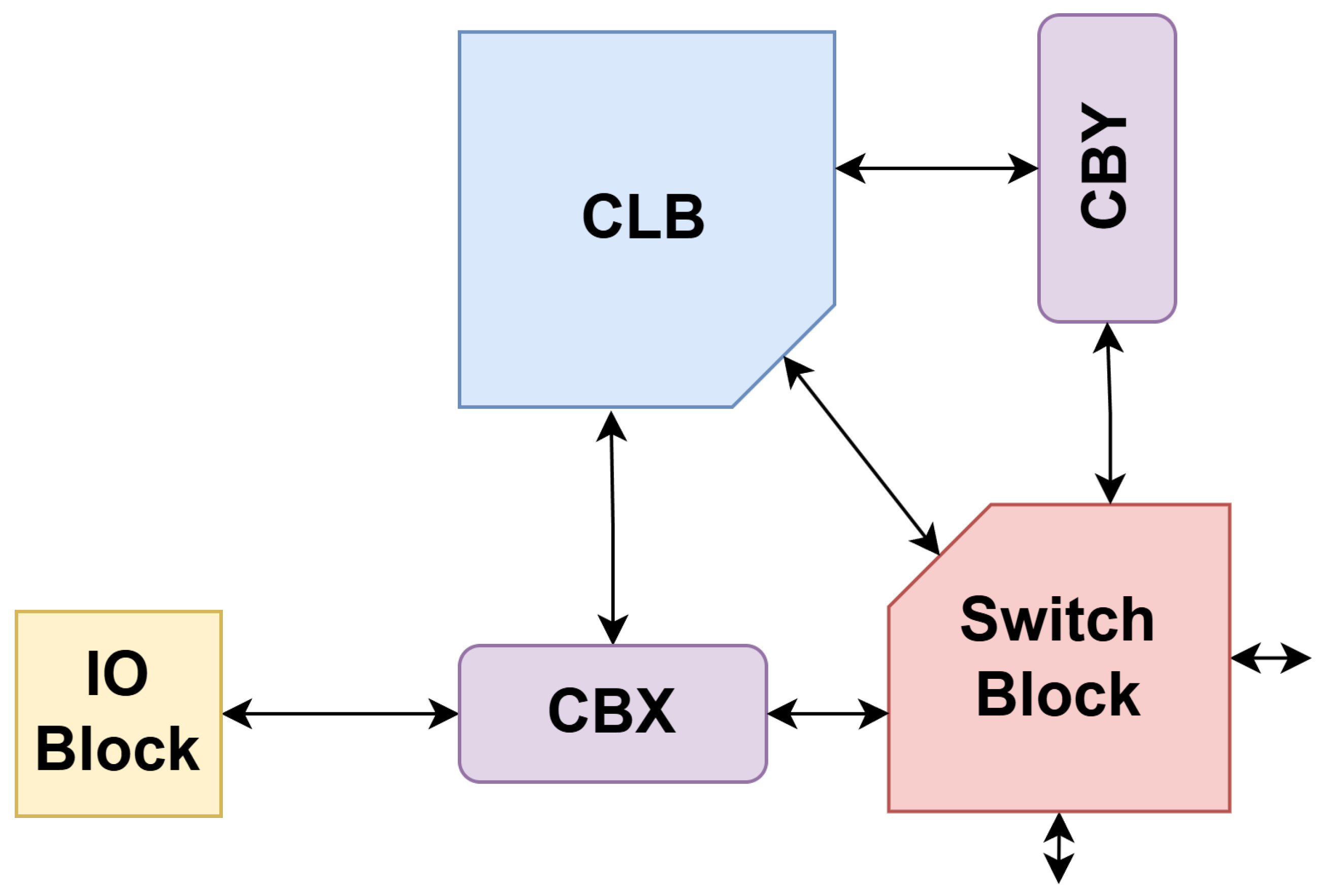
The macro placement configuration file is a crucial document that defines the placement of each module within the FPGA architecture. It specifies the coordinates for various components such as switching blocks, x and y connection blocks, CLBs, I/O blocks, and any other relevant blocks. Each module is assigned its own unique coordinate, which determines its physical location within the FPGA fabric. It is essential to ensure that modules are properly spaced to avoid routing congestion issues. Additionally, modules should not overlap or encroach upon the space allocated for other modules to ensure proper functionality and prevent any potential conflicts during the placement process. By carefully defining the coordinates and allocating sufficient space for each module, designers can achieve optimized placement and mitigate routing congestion challenges in the FPGA design.
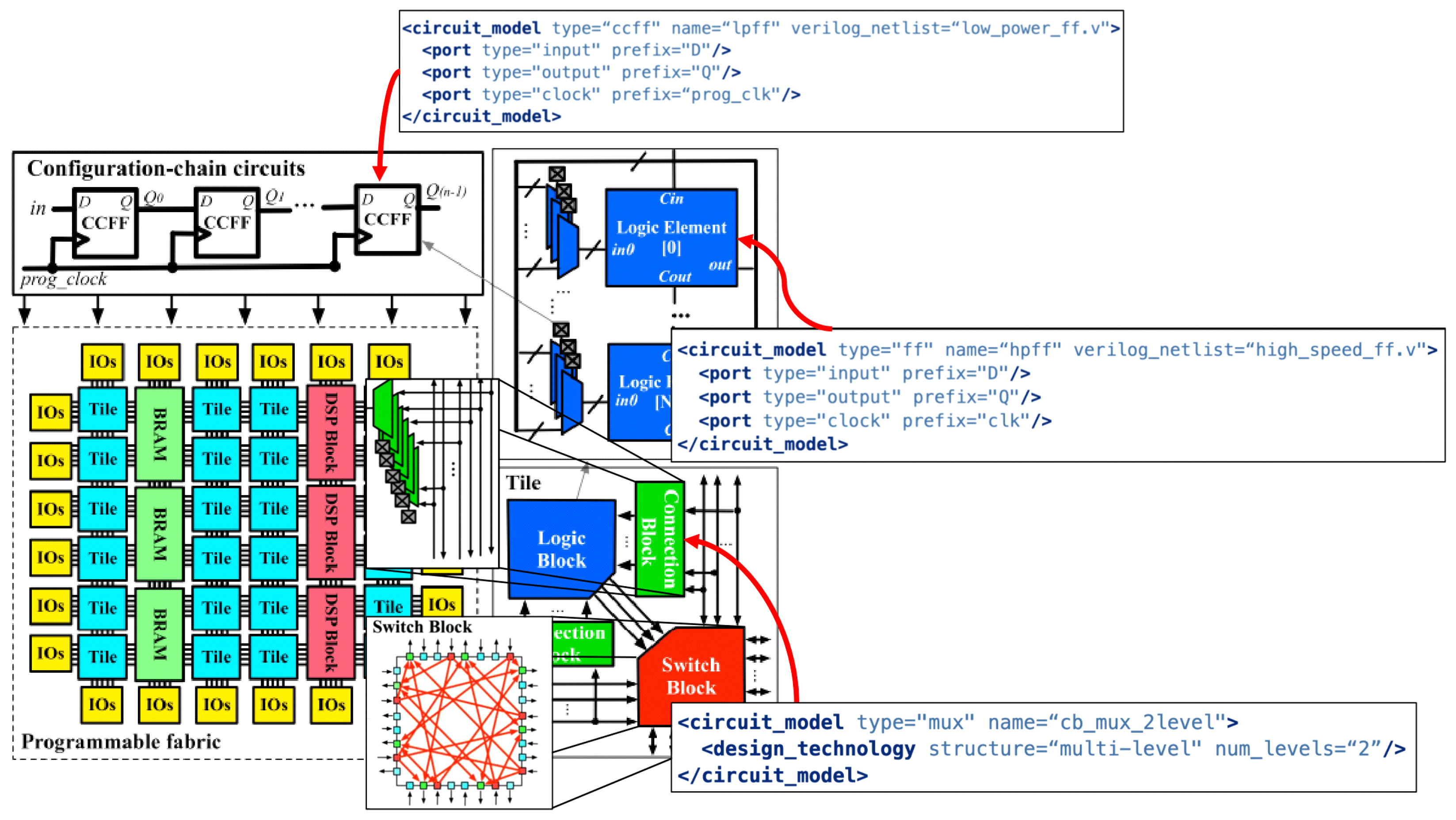
To streamline the process of macro placement in the FPGA design, a Python 3.8 script has been developed. This script simplifies the placement task by taking input parameters specifying the maximum sizes of x and y connection blocks, CLBs, and switching blocks. Based on these sizes, a perimeter is generated, as depicted the tile in
Figure 6, which is the FPGA architecture and serves as the boundary for the placement of tiles.
The dimensions of the basic tile perimeter are calculated, and the coordinates of each tile are adjusted accordingly, considering the position of the tile within the FPGA fabric. Additionally, the script includes parameters for specifying the spacing between cells in the x and y directions. However, it is important to note that while the script automates much of the floorplanning process, it still requires manual verification and adjustment to ensure optimal placement and address any specific floorplanning considerations or constraints.
3.7. Analysis of Core-Level Configuration in FPGA Design
To initiate the design process for the core module (
FPGA_top), the first step involves creating a new OpenLane project. It is essential to adhere to the OpenLane workflow and treat the
FPGA_Top module as a core entity. The project configuration requires specifying various basic parameters, which can be found in [
19]. These configuration parameters include
DESIGN_NAME,
VERILOG_FILES,
CLOCK_PORT,
CLOCK_PERIOD,
FP_PDN_MULTILAYER,
EXTRA_LEFS,
EXTRA_GDS_FILES,
VERILOG_FILES_BLACKBOX,
FP_SIZING,
DIE_AREA,
RT_MAX_LAYER,
VDD_NETS,
GND_NETS, and
FP_PDN_MACRO_HOOKS.
After selecting the basic parameters for a successful RTL-to-GDSII conversion, it is recommended to configure additional parameters for optimal results. These configurations can help fine-tune the OpenLane flow and achieve desired outcomes. The following parameter settings are suggested:
FP_PDN_CHECK_NODES = 0: Disables checking nodes during floor planning PDN generation.
SYNTH_ELABORATE_ONLY = 1: Enables only synthesis elaboration without running further steps in the flow.
PL_RANDOM_GLB_PLACEMENT = 1: Enables random placement of Global Logic Blocks (GLBs) during placement.
PL_RESIZER_DESIGN_OPTIMIZATIONS = 0: Disables design optimizations during placement.
PL_RESIZER_TIMING_OPTIMIZATIONS = 0: Disables timing optimizations during placement.
PL_RESIZER_BUFFER_INPUT_PORTS = 0: Disables adding buffer input ports during placement.
FP_PDN_ENABLE_RAILS = 0: Disables enabling rails for floorplan power distribution network.
DIODE_INSERTION_STRATEGY = 0: Uses the default strategy for diode insertion.
RUN_FILL_INSERTION = 0: Disables fill insertion step.
RUN_TAP_DECAP_INSERTION = 0: Disables tap decap insertion step.
CLOCK_TREE_SYNTH = 0: Disables clock tree synthesis step.
MAGIC_ZEROIZE_ORIGIN = 0: Disables setting the origin for the Magic database.
These parameter configurations can be adjusted based on the specific requirements of the design. For macro hardening, OpenLane provides features to customize the hardening process. It involves optimizing and hardening individual macros or modules to improve their performance and reliability. The OpenLane documentation provides detailed explanations of each parameter and its impact on the macro hardening process. By carefully configuring these parameters, designers can achieve efficient macro hardening and fine-tune the FPGA design to meet their specific goals.
The remaining configurations are related to the PDN. To address PDN issues, it is recommended to examine the FP_PDN variables. These variables allow for fine-tuning and customization of the PDN generation process.
3.8. Analysis of Gate-Level Simulation for Functional Validation
After completing the RTL-to-GDSII flow, a variety of files will be generated. If the workflow is successful, you can locate the Verilog files in the result/final/Verilog directory of OpenLane. These Verilog files are specifically designed to be compatible with SKY130 logic cells. With these Verilog files, you can now perform the same full testbench, but at the gate level. This allows for comprehensive testing and verification of the synthesized design using the specific SKY130 PDK.
4. Case Study
This case study explores the development of a custom FPGA architecture capable of implementing basic logic gates and arithmetic operations. The primary goal is to design a replicable FPGA architecture that is accessible to a wide audience. To achieve this, the case study will be a small FPGA that can be replicated with low-performance equipment and open-source tools, allowing anyone to follow the design flow and create their own custom FPGA design. While the approach is tailored for simplicity and accessibility, it is also scalable, allowing for the creation of larger and more complex FPGA architectures. However, scaling up may require more advanced resources and commercial simulation tools, as open-source simulators are currently limited to single-core execution, which can take long processing time for more intricate designs.
The case utilizes OpenFPGA to customize the FPGA architecture using the semi-customized approach, tailoring it to meet the specific requirements to execute the basic arithmetic operation. Through the use of XML files and the structure, functionality, and physical characteristics of the FPGA design are defined. After architecture design, a full testbench validates performance by configuring the FPGA to run logic gates as well as addition and subtraction.
The physical design process leverages OpenLane’s RTL-to-GDSII flow, which facilitates the synthesis, placement, and routing of the FPGA design at layout. Following the recommended configurations and parameters, as outlined in the previous sections, ensures an optimized and reliable implementation.
This case study exemplifies the practical application of OpenFPGA and OpenLane, open-source tools, in the development of custom FPGA architectures at layout. The ultimate result of the RTL-to-GDSII flow is the creation of a finalized GDSII file, representing a design that is ready for manufacturing. This successful translation of the custom FPGA architecture into a tangible hardware implementation highlights the potential of open-source tools in democratizing FPGA development and enabling innovation in the field of hardware acceleration.
4.1. Case Study: Analysis of FPGA Architecture Customization with OpenFPGA
For the development of this FPGA, a semi-customized approach was utilized, building upon the
k4_N4 architecture provided by OpenFPGA. This configuration incorporates an FPGA structure with I/O blocks positioned along the perimeter, encircling the CLBs. Each CLB is composed of four LUTs, each supporting four inputs. Modifications to this architecture include the adoption of a 3 × 3 CLB arrangement, the use of a single I/O per I/O block, and the incorporation of a tileable design that maximizes the reuse of submodules.
Figure 7 illustrates this architecture.
4.2. Case Study: Analysis of Functional Verification Using Full Testbench
One key feature of OpenFPGA is its ability to generate a complete testbench that combines both the configuration and operating phases, as discussed in previous sections. It is important to note that the generated testbench sets up the environment to send the bitstream and configure the FPGA. Once the FPGA is configured, a series of random values are sent to all of its inputs, which is suitable for simple arithmetic and logic operations. However, this approach may not be ideal for more complex systems or protocol communication. In such cases, it is recommended to modify the testbench provided by OpenFPGA to better suit specific requirements.
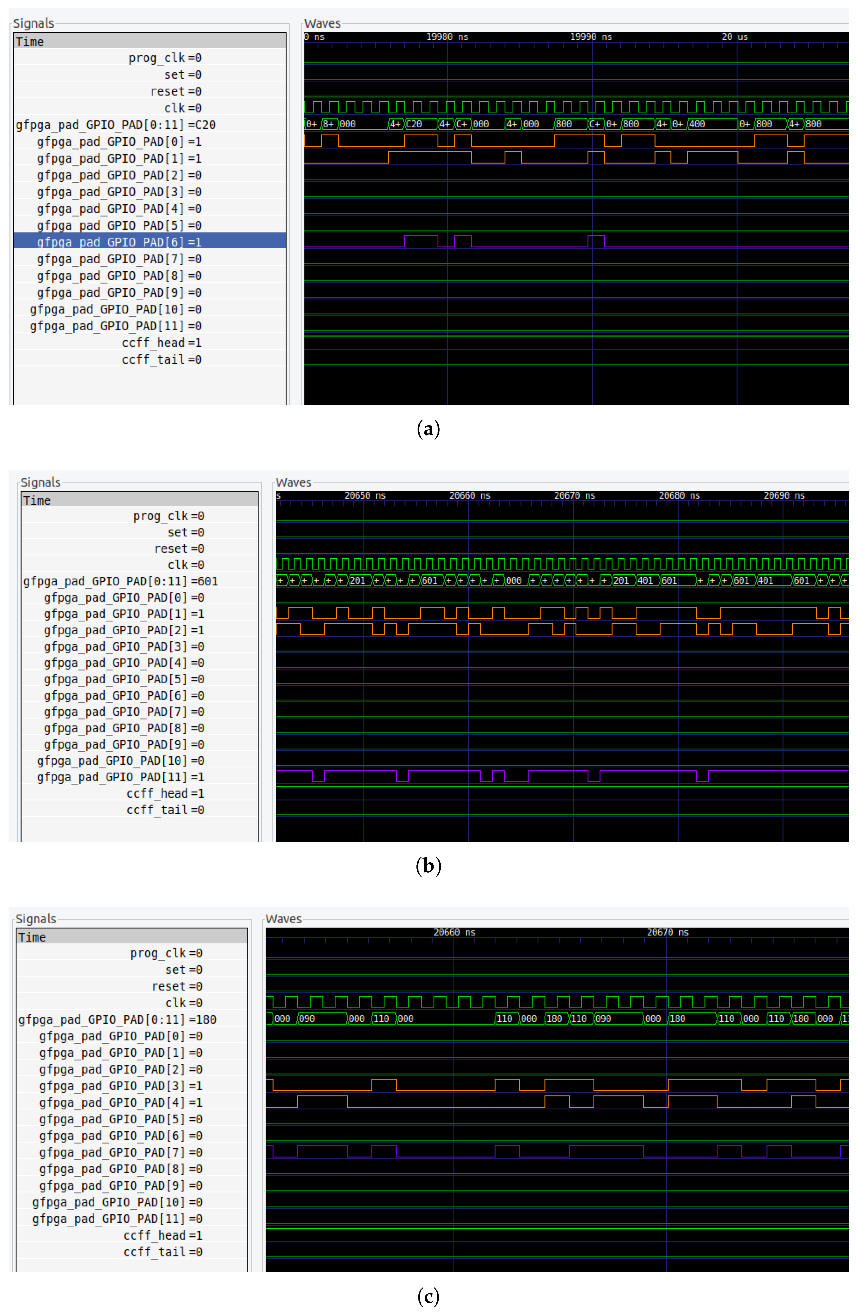
Figure 8a shows the
configuration phase testbench of the FPGA when it is configured as an AND gate. The figure highlights five control signals:
prog_clk, the clock used during FPGA configuration;
ccff_head (also known as the Configuration Chain Flip-flop or ccff), which serves as the input to send the bitstream (one bit for this architecture);
set and
reset signals, used to initialize the FPGA state; and finally,
ccff_tail, which acts as an output signal indicating when the FPGA has been successfully configured.
Figure 8b illustrates the
operating phase, where
GPIOs [0] and
[1] are used as the inputs for the AND gate, and
GPIO [6] serves as the output of the AND gate.
4.3. Case Study: Analysis of Macro-Level RTL-to-GDSII Implementation
Before starting the RTL-to-GDSII flow with OpenLane, it is important to organize the Verilog files into their respective main modules. To achieve this, refer to the fabric_hierarchy.txt file provided by OpenFPGA. For this case, the primary modules that compose the FPGA_top are
grid_io_top grid_io_right grid_io_bottom grid_io_left grid_clb sb_0__0_ sb_0__1_
| sb_0__3_ sb_1__0_ sb_1__1_ sb_1__3_ sb_3__0_ sb_3__1_ sb_3__3_
| cbx_1__0_ cbx_1__1_ cbx_1__3_ cby_0__1_ cby_1__1_ cby_3__1_
|
Note that modules containing the word “io” in their name refer to the I/O blocks, “clb” refers to the CLBs, “sb” denotes the switching block modules, and “cb” represents the connection blocks for the “x” and “y” directions.
The next step is the verilog file modification of the previous modules adding the the <power_pin> and <ground_pin>; e.g., the grid_io_top.v will change from Listing 1 to Listing 2.
| Listing 1. Verilog code prior to power port modification, showing instantiation via positional association. |
![Electronics 14 03866 i001 Electronics 14 03866 i001]() |
| Listing 2. Verilog code after power port modification, showing instantiation via named association. |
![Electronics 14 03866 i002 Electronics 14 03866 i002]() |
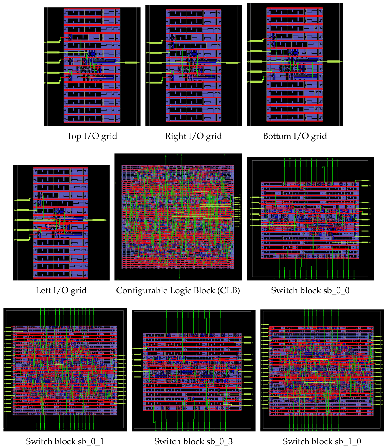
Now, we can import the FPGA Verilog files into OpenLane, where we can obtain the layout of the main modules.
Section 3.5 provides the essential configuration required to achieve a successful macro layout. For example, the following
config.json file was used to generate the
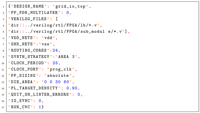
grid_io_top tile layout as Listing 3 illustrates; remember that OpenLane uses the
config.json to execute the RTL-to-GDSII flow.
| Listing 3. JSON configuration used in OpenLane to harden the grid_io_top macro. |
![Electronics 14 03866 i003 Electronics 14 03866 i003]() |
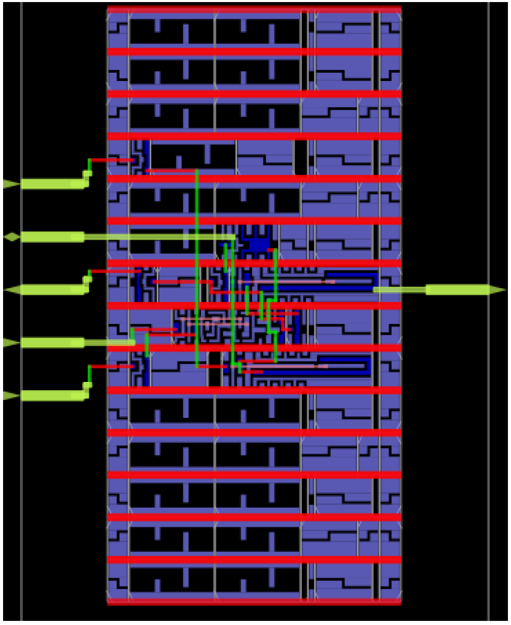
Figure 9 illustrates the layout obtained after the OpenLane execution.
This process must be repeated for the primary modules that compose the FPGA_top.
4.4. Case Study: Analysis of Core-Level RTL-to-GDSII Integration
The initial step involves grouping the files generated by each macro, as these files are essential for producing the final layout. After file organization, we configure the
config.json file with the parameters detailed in
Section 3.6 and
Section 3.7. Particular attention must be paid to the
FP_PDN_MACRO_HOOKS and
MACRO_PLACEMENT_CFG configurations.
The FP_PDN_MACRO_HOOKS parameter (Listing 4) establishes explicit connections for the voltage and ground pins that were incorporated in the Verilog files using USE_POWER_PINS. The asterisk (*) denotes that all modules with the specified name will be connected, as shown in the following configuration example:
| Listing 4. JSON configuration of FP_PDN_MACRO_HOOKS in OpenLane, where * is used as a wildcard to apply power and ground connections to matching modules. |
![Electronics 14 03866 i004 Electronics 14 03866 i004]() |
Conversely, the MACRO_PLACEMENT_CFG parameter (Listing 5) references a macro.cfg file containing coordinate strings that determine the placement of each macro instantiated in the top module. The configuration fragment below illustrates this:
| Listing 5. Fragment of the macro.cfg file in OpenLane, specifying placement coordinates and orientations for top-level macros. |
![Electronics 14 03866 i005 Electronics 14 03866 i005]() |
In this example, the macro
sb_0__0_ is positioned at coordinates (x = 300, y = 241) within the area defined by the
DIE_AREA parameter.
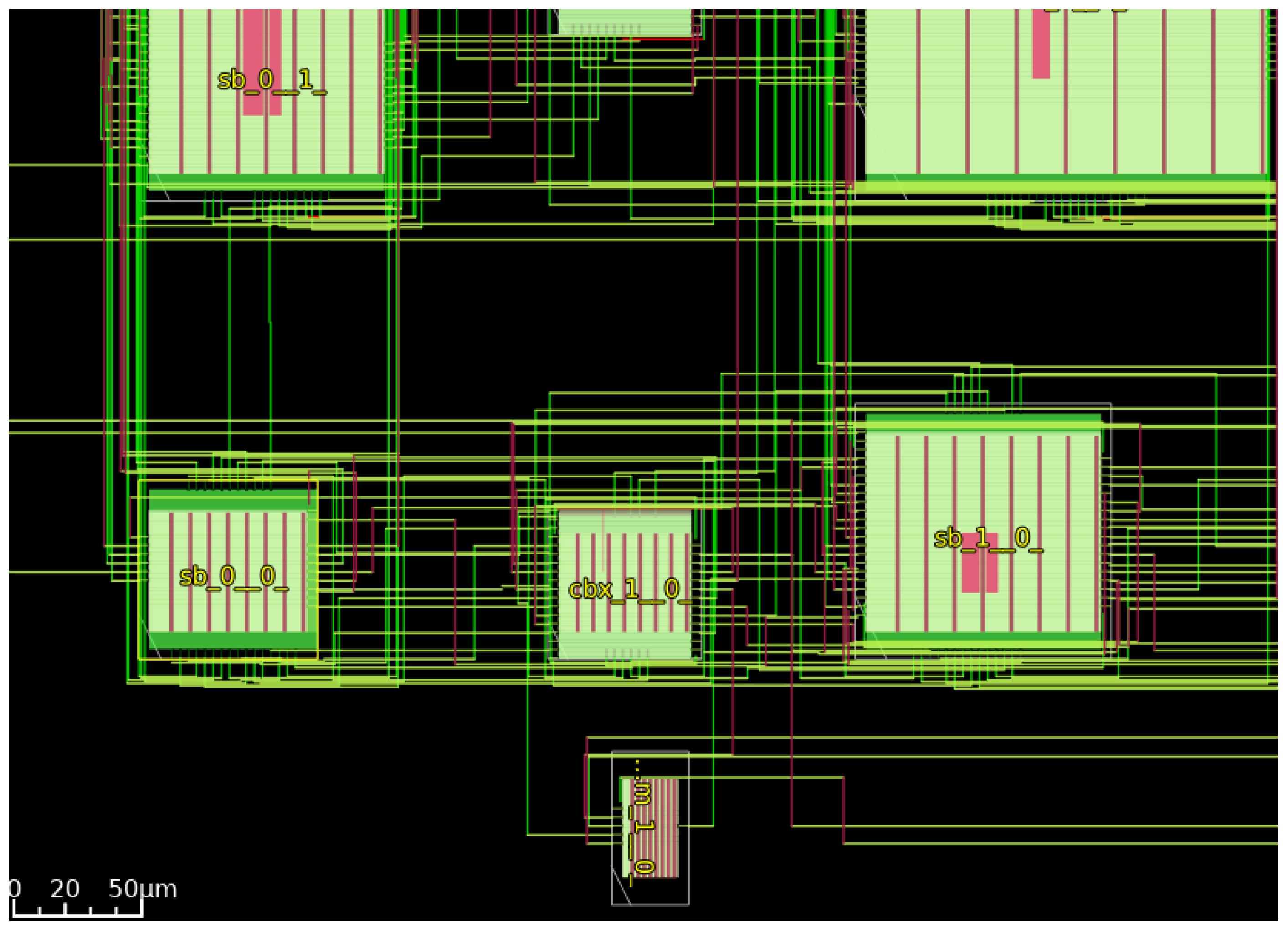
Figure 10 displays a portion of the
FPGA_top layout after the correct execution of the RTL-to-GDSII flow, demonstrating the placement of modules
sb_0__0_,
sb_1__0_,
cbx_1__0_,
grid_io_bottom_1__0_, and
sb_0__1_ according to the
macro.cfg specifications.
The configuration files mentioned in
Section 4.3 and
Section 4.4 can be found in the [
24] GitHub repository commit bb57e04.
6. Discussion
This work demonstrates that a fully open-source toolchain (specifically OpenFPGA [
8] and OpenLane [
19]) can implement a semi-custom embedded FPGA from RTL to a manufacturable GDSII, with the resulting layout verified at the gate level in SKY130. An alternative option for implementing custom FPGA RTL is the FABulous framework [
11], which has been successfully employed in prior works. However, in the present study, FABulous was not adopted, as it does not provide SDC file generation, a feature essential for seamless integration with back-end physical design flows. A comparative evaluation of FABulous and OpenFPGA would nevertheless be valuable in future work, as it could highlight differences in usability, reproducibility, and flow automation. On the other hand, frameworks such as PRGA [
12] and Archipelago [
25] were also not considered in this study, as they require significantly more manual effort—particularly in generating testbenches—thus complicating reproducibility and increasing the barrier to entry for new users.
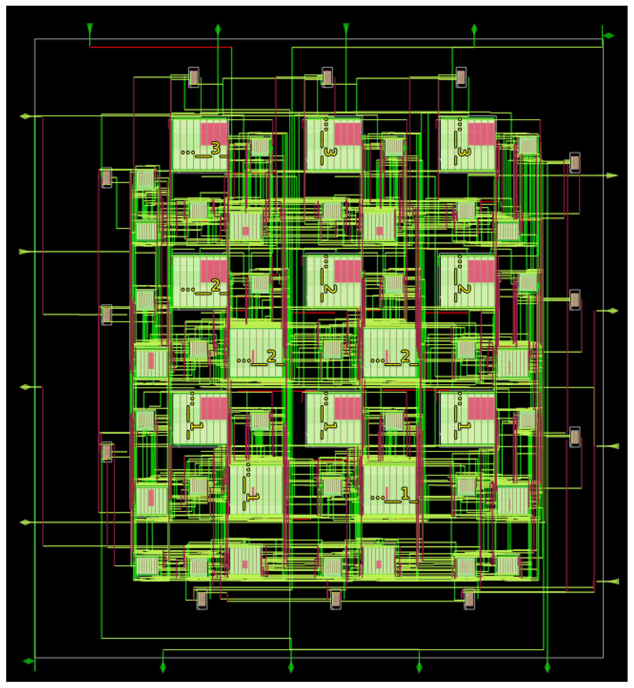
In the presented workflow, OpenLane automatically routes the hardened macros within the 3 × 3 CLB fabric (
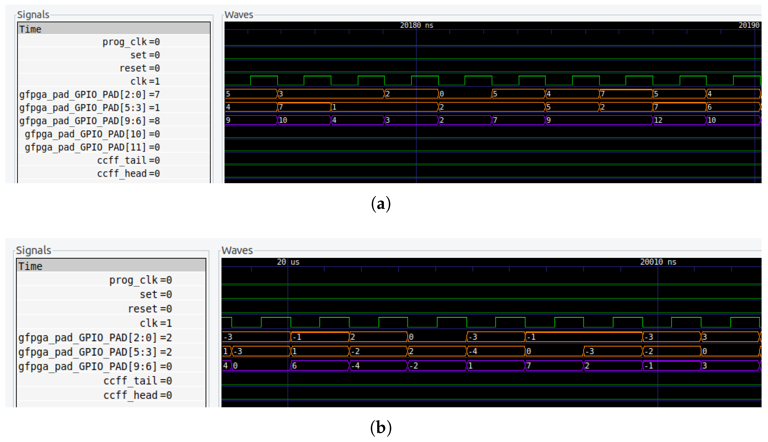
Figure 11) by leveraging the defined floorplanning constraints, while gate-level simulations confirm correct logical (AND/OR/XOR) and arithmetic (add/sub) functionality after technology mapping to standard cells (
Figure 12 and
Figure 13). These system-level results show that the architectural intent specified in OpenFPGA is faithfully preserved through physical synthesis and sign-off in OpenLane.
A notable practical finding is the emphasis on reproducible macro hardening and the correct interconnection among the hardened blocks, as illustrated in
Figure 6 and
Figure 7. At the macro level, the principal components of the fabric—including I/Os, CLBs, and switch and connection blocks—were individually hardened; the complete set is enumerated in
Appendix A. As reported in
Section 5, a total of 20 macros were successfully realized at the layout stage, enabling floorplanning and routing of the top-level integration.
The size contrast between the larger tiles (e.g.,
grid_clb,
sb_0__0_) and the smaller I/O tiles along the periphery helps explain the placement and routing pattern observed in
Figure 11. In particular, the dimensions of the connection and switching blocks could not be reduced further without changing the RTL architecture, as their size is mainly determined by the number of I/Os required per tile and by the minimum spacing restrictions that must be respected in the layout between adjacent I/Os; a flat implementation (without macros) of connection and switching blocks often worsens routing, causing routing congestion. In relation to the size of CLB, it arises because OpenLane synthesizes memories as large groups of registers; since LUTs are inherently memory elements and each CLB contains many LUTs, a substantial portion of the CLB area is consumed by registers. While this could be alleviated through the use of small custom memory macros, such an approach would require advanced handling of mixed signals as well as specialized expertise in memory architecture and analog layout design.
Related to the OpenLane constraints and configuration, two configurations were essential for clean integration in OpenLane: explicit macro power hooking and scripted macro placement. The use of FP_PDN_MACRO_HOOKS ensured consistent power/ground stitching across all major tile families, while a macro.cfg with Python-generated coordinates enforced spacing and orientation, preventing overlaps and reducing congestion. These measures enabled automated placement without manual adjustments. Parameter choices also influenced routability and verification effort: high placement density (PL_TARGET_DENSITY = 0.90) was feasible for small macros but problematic at larger scales. Finally, running the full gate-level testbench with SKY130 models was critical to detect RTL integration mismatches in the flow.
Relative to prior research [
2,
7,
8,
9,
11], our contribution is to document a comprehensive RTL-to-GDSII workflow, from RTL design to layout configuration—floorplanning decisions, PDN hooks, placement files, routing, and GL simulation. Another layout embedded FPGA implementations [
7,
9] and advanced automatic floorplan but did not comprehensively expose routability/clocking options or runtime/memory considerations, which complicates replication by newcomers; additionally, much of the literature still relies on proprietary PDKs under NDA, curbing transparency. Our workflow is demonstrated entirely with an open PDK and includes concrete config fragments to lower the barrier to reproduction, enabling new researchers to incorporate and experiment with embedded FPGAs in their designs.
The present validation was conducted using SKY130, one of three currently fabricable open PDKs (alongside GF180MCU [
15] and IHP-130 [
16]). While portability to other nodes is plausible, it is not guaranteed, as differences in metal stacks, antenna rules, and routing resources may require re-tuning of floorplan dimensions, PDN pitches, and diode insertion strategies. Although OpenROAD-based [
21] flows support multiple PDKs, OpenLane’s [
19] higher level of automation and the use of our predefined templates were preferred to reduce development time. A further consideration is scalability: open-source simulators and verification tools can become runtime bottlenecks for larger fabrics (e.g., single-core execution in certain steps). This highlights the need for modular testbenches and partitioned gate-level checks to maintain efficiency as design complexity increases.
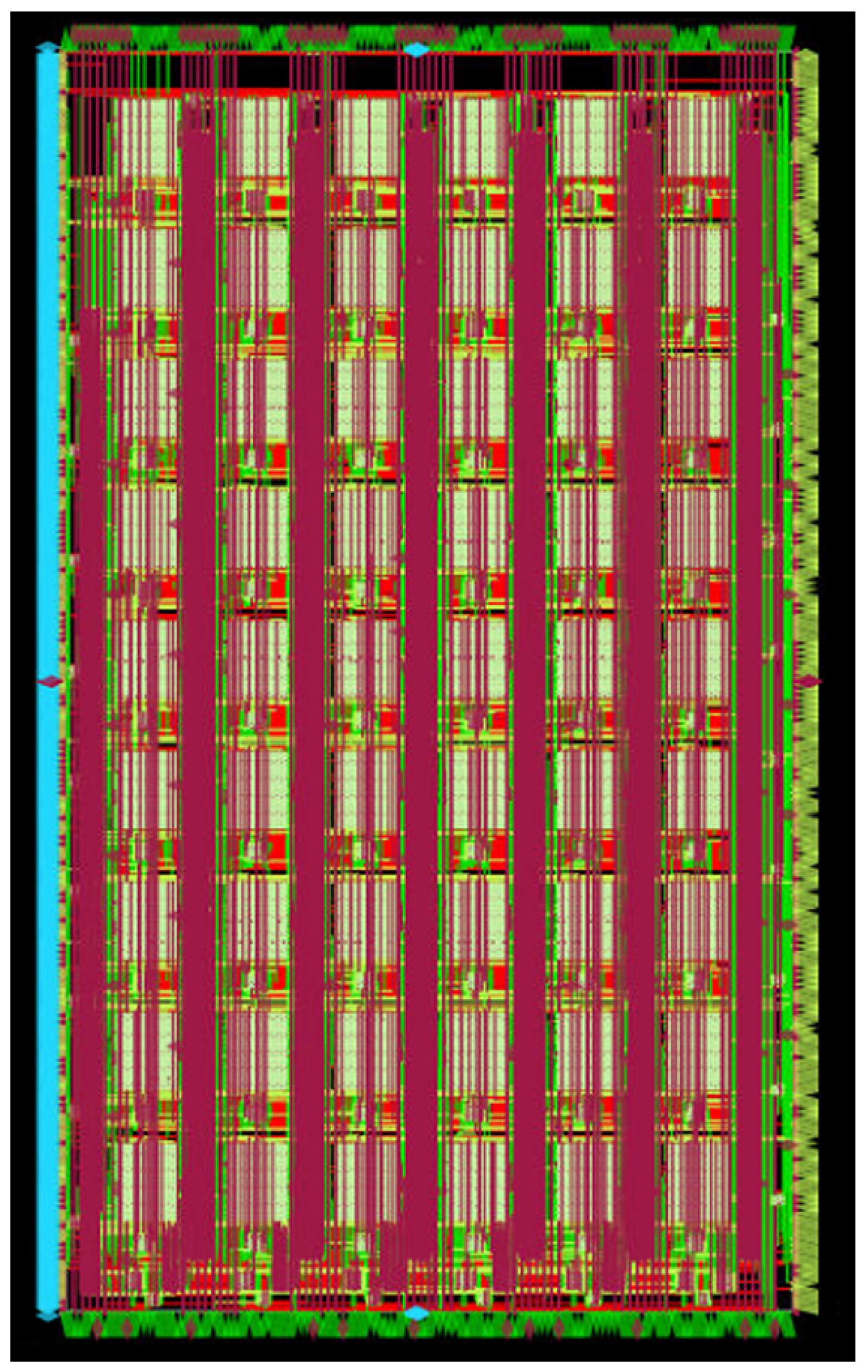
In addition to the 3 × 3 CLB case study, we have extended the validation with a larger implementation to illustrate scalability of the flow. Specifically, a layout of an FPGA fabric comprising 540 six-input LUTs has been generated (
Figure A1), demonstrating that the OpenFPGA/OpenLane toolchain can handle designs of significantly greater size and complexity beyond the small-scale prototype. This larger case highlights runtime and resource trends consistent with expectations: placement density and routing congestion increase with fabric size, but the flow remains functional when aided by scripted macro placement and explicit PDN hooks. As discussed above, scalability is ultimately limited by simulator runtime and verification overhead; however, the successful integration of a fabric with hundreds of LUTs confirms the applicability of the methodology to more general and industrially relevant scenarios.
While the workflow demonstrates functional correctness and scalability, reliability remains a critical dimension for mission-critical applications such as aerospace, automotive, and secure communications. Open-source tools like OpenLane and OpenFPGA do not yet natively support advanced reliability features, including automatic DFT, built-in self-test, or fault-tolerance mechanisms against single event upsets. These aspects are particularly relevant when targeting safety-critical or radiation-prone environments, where robustness must be validated through fault injection campaigns, redundancy strategies, and rigorous verification using edge cases. Although some manual methods (e.g., scan chain insertion) have been reported, integrating them seamlessly into the open-source RTL-to-GDSII flow remains an open challenge. Addressing these gaps would strengthen the applicability of the proposed methodology to industrial sectors that demand not only performance but also resilience and long-term reliability.
Practical guidance distilled from this study includes the following: (i) add
USE_POWER_PINS to all macro RTL and verify uniform net names before synthesis; (ii) keep a single source of truth (
macro.cfg) for tile coordinates and orientations and regenerate it from parameters rather than editing by hand; (iii) begin with conservative density and progressively enable optimization passes as macros converge; and (iv) always replicate the “full testbench” at the gate level with the target PDK models before moving to tapeout collateral. Our artifact repository referenced in [
24] contains the exact configuration files used for macro/core hardening and can serve as a starting point for replication or extension.


