Article

Channel Temperature Measurement of GaN HEMT Used in Kilowatt-Level Power Amplifier

1
Department of Engineering Physics, Tsinghua University, Beijing 100084, China
2
Science and Technology on High Power Microwave Laboratory, Northwest Institute of Nuclear Technology, Xi’an 710024, China
*
Author to whom correspondence should be addressed.
Electronics 2025, 14(19), 3861; https://doi.org/10.3390/electronics14193861
Submission received: 9 September 2025 / Revised: 26 September 2025 / Accepted: 26 September 2025 / Published: 29 September 2025

Abstract

This paper presents an electrical thermometry method designed for kilowatt(kW)-level Gallium Nitride (GaN) High Electron Mobility Transistors (HEMTs). The dependence of the drain current on the channel temperature in GaN HEMTs is utilized as a means to measure the transient channel temperature. However, in kW-class GaN HEMTs, the gate current can reach tens of milliamperes, and trap-induced capture resulting from high doping concentrations can both influence the drain current. Through modifications to the gate bias circuit, the gate voltage self-biasing phenomenon caused by the gate current is mitigated. A theoretical model is derived to express the relationship between the drain current and the channel temperature. Experimentally, amplifier modules equipped with kW-level HEMTs were placed on thermal stages set at 45 °C, 60 °C, and 80 °C. The transient drain current curves and the corresponding channel temperature profiles were measured. The measured drain current versus channel temperature curves at different ambient temperatures were fitted and compared with the theoretically derived formula. The relative error between the measured and calculated drain current values at the same channel temperature was found to be within 1%.

1. Introduction

Gallium Nitride (GaN) semiconductors offer advantages such as high electron saturation velocity and high breakdown electric field strength, making them widely used in high-power microwave power amplifiers [1,2]. In recent years, with applications in deep-space exploration and phased array radar systems, GaN HEMTs have been progressively miniaturized and integrated, while their output power has been increased to the kilowatt (kW) level [3]. For kW-level GaN HEMTs, high power density leads to significant heat generation. Sustained heat accumulation causes a rapid rise in temperature, resulting in performance degradation. Excessive temperature may even cause thermal breakdown and failure [4]. Therefore, temperature is a key factor limiting further increases in the power capacity of GaN HEMTs. To prevent excessively high operating temperatures due to continuous heat accumulation, these power amplifiers are often operated under narrow-pulse-width and low-duty-cycle conditions. Consequently, for kW-level GaN HEMTs, temperature measurement under narrow pulses and low duty cycles is crucial for the reliability of design and engineering applications of high-power microwave power amplifiers [5].
There are three main approaches to temperature measurement of GaN HEMTs:
(1)
Optical temperature measurement techniques: such as infrared thermography, Raman spectroscopy, and thermoreflectance imaging, can directly acquire die-temperature data [6]. However, optical thermometers with microsecond-level temporal resolution and micrometer-level spatial resolution are extremely expensive and often require dedicated device samples and specialized equipment [7], which are generally inaccessible in many electronics laboratories.
(2)
Three-dimensional modeling and simulation: constructing a three-dimensional finite element model based on the HEMT’s structure and material parameters to simulate the temperature distribution [8,9]. The advantage of this approach is the rapid acquisition of temperature profiles with extremely high spatial resolution. Nevertheless, accurate simulation requires precise structural dimensions of the transistor, which are often not fully disclosed by manufacturers due to confidentiality issues. Moreover, most mainstream thermal simulation software relies on Fourier’s law, which has certain limitations at micrometer-scale dimensions, making it difficult to accurately predict heat transfer processes [10].
(3)
Electrical measurements: indirect identification procedures from electrical measurements [11,12], which indirectly measure the temperature based on the dependence of electrical parameters on temperature. It is usually measured through electrical parameters with higher temperature sensitivity, such as threshold voltage and drain current [13,14]. The advantage of the electrical measurement method is that it can be rapidly measured using standard equipment and does not require direct contact with the power amplifier. Nevertheless, there are multiple factors influencing kW-class GaN HEMTs, such as the relatively large gate leakage current affecting the gate voltage and the trap effect influencing the drain current [15,16]. As a result, temperature is no longer a single variable of the drain current, making it difficult to accurately reflect the temperature variation by measuring the drain current.
For the first time, this study presents an electrical measurement method designed for kW-level GaN HEMTs. Modifying the series resistor and parallel capacitor in the gate bias circuit minimizes the gate leakage current’s influence on the gate voltage, thereby reducing its impact on the drain current. The drain current waveforms were measured using a current clamp under ambient temperatures of 45 °C, 60 °C, and 80 °C, while the corresponding channel temperature was monitored by infrared thermography. A temperature-dependent current variation formula was derived based on experimental data at 45 °C. This formula was then used to establish a fitting model describing the relationship between current and temperature. The trap capture constant of the kW-level GaN HEMT was determined by comparing the formula-derived curves with experimental results. Furthermore, the validity of the fitting model was confirmed under conditions without trap effects, demonstrating its ability to accurately characterize current variations with channel temperature across different ambient temperatures. Consequently, real-time temperature estimation can be achieved by monitoring transient drain currents.

2. Detailed Analysis of the Proposed Method

2.1. Derivation of Drain Current Equations

In a high-power GaN HEMT, the directional movement of two-dimensional electron gas in the channel forms the drain current, and the electron concentration ns can be expressed as [17]:
n s X , Y = ε x q d + D V G V T V Y
where ε(x) is the dielectric constant of the AlGaN layer, q is the elementary charge, d is the thickness of the AlGaN barrier layer, D is the channel thickness, VG is the gate voltage, V(Y) is the potential distribution along the channel length, and VT is the threshold voltage. By integrating the electron concentration along the channel length (Y-direction), the drain current Ids is derived as [18]:
I d s    = 0 L q n s X , Y W v E d Y     = 0 L q n s X , Y W μ E d Y   = 0 L q n s X , Y W μ d V          = 0 L W μ ε x d + D V G V T V Y d V         = W μ ε x 2 L d + D 2 V G V T V d s V d s 2
where W is the gate width, L is the channel length, μ is the electron mobility, and Vds is the drain voltage. When d I d s / d V d s = 0 , the solution yield is V d s = V G V T . The physical quantities that change with temperature in the drain current expression formula include electron mobility μ(T) and threshold voltage VT(T) [19]. When the power amplifier works in the saturation region, V d s V G V T , the drain current Ids(T) formula can be expressed as:
I d s T = W μ T ε x 2 L d + D V G V T T 2
where Ids(T), μ(T) and VT(T) is the drain current, carrier mobility, and threshold voltage at the channel temperature T. Electron mobility μ(T) decreases with increasing temperature, and its change with temperature can be described as [20]:
μ T = μ T 0 T T 0 k 1
where T is the channel temperature, T0 is the ambient temperature, μ(T0) is the electron mobility at the ambient temperature T0 and k1 is a constant. The threshold voltage of the HEMT decreases almost linearly with increasing temperature and can be described as [20]:
V T T = V T T 0 k 2 T T 0
where VT(T0) is the threshold voltage at a channel temperature of T0 and k2 is a constant. Therefore, as the temperature increases, the drain current will decrease as the carrier mobility decreases, and increase as the threshold voltage decreases. When the drain current is large, the carrier mobility change caused by temperature change has a greater effect on the drain current. When the drain current is small, the influence of threshold voltage is greater.
For a GaN HEMT with output power up to kilowatts, the drain current generally ranges from tens of amps to hundreds of amps. The main reason for the drain current change is carrier mobility, and the threshold voltage change is relatively negligible. Consequently, the relationship between drain current Ids(T) and temperature can be expressed as [21]:
I d s T = I d s T 0 T T 0 k
where Ids(T0) is the drain current at a channel temperature of T0.

2.2. Key Factors Influencing Drain Current

For a GaN HEMT, when an external pulsed voltage signal is applied, Ids represents the response to the Vds excitation, exhibiting a trend depicted in Figure 1a. As derived from Formulas (2) and (3), Ids is primarily dependent on the Vgs, trap effects, and temperature [22,23].

2.2.1. Gate Voltage

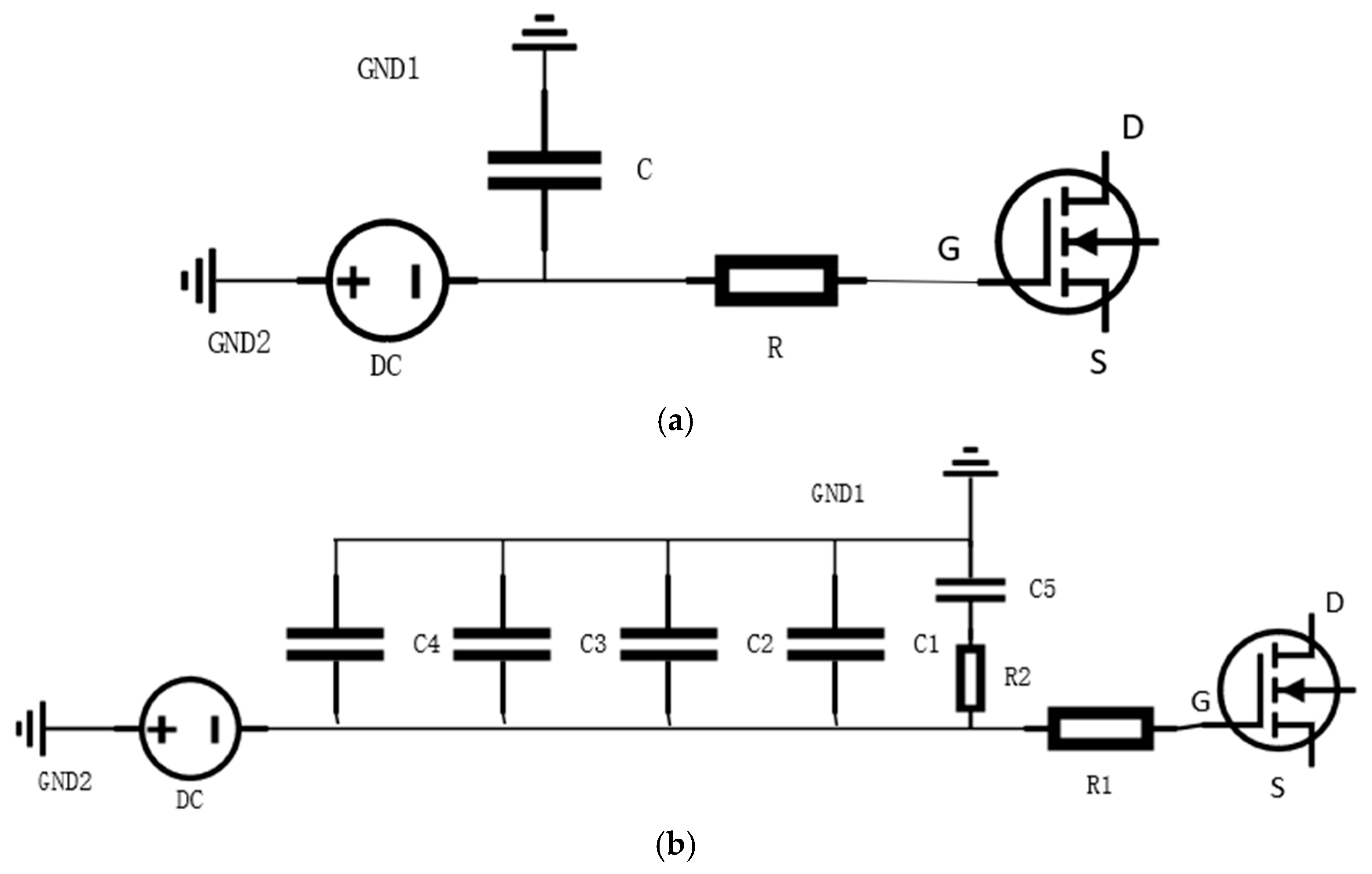
Experiments have revealed that GaN HEMTs exhibit a significant number of defects, with a surface state trap density at the AlGaN/GaN interface of approximately 1013 cm−2 [24]. The gate leakage current and carrier concentration are correlated with the surface state trap density [25]. As a result, kW-level GaN HEMTs exhibit substantial gate leakage current. This gate current induces a voltage drop across the gate bias circuit, thereby affecting the gate voltage. Reducing the resistance of the gate bias circuit can mitigate variations in the gate voltage. To counteract the negative resistance effect, GaN HEMTs require a stabilized gate bias circuit, typically implemented using an RC parallel structure [26]. This study modifies the conventional RC parallel circuit composed of a 4.7 Ω resistor and a 10 μF capacitor by reducing the gate resistor to 0.5 Ω and increasing the number of parallel capacitors. The circuit schematic is shown in Figure 2. At high frequencies, capacitors exhibit parasitic resistance and inductance. Figure 3 shows the simulated frequency-dependent S-parameters obtained using ADS 2022 software. The optimized design demonstrates improved filtering performance in the gate bias circuit. The resistance and capacitance values of the modified bias circuit were selected based on the oscillation frequency observed without the bias circuit, and this method is scalable to different power levels.

2.2.2. Trap Effect

When Vgs remains constant within the drain voltage pulse, Ids is predominantly influenced by trap effects and temperature. It is generally acknowledged that trap capture occurs within a very short duration (approximately 50 ns) after the application of the drain pulse voltage [27], but this process is sufficiently rapid to elude detection by even the most advanced narrow-pulse measurement systems. However, Ref. [28] revealed the existence of trap capture with millisecond-level time constants (τ) in a GaN HEMT. The temperature impact on Ids encompasses both ambient temperature and self-heating-induced temperature rise. For pulsed-power amplifiers, self-heating causes the junction temperature to increase gradually during the pulse, consequently leading to a monotonic decrease in Ids over time.
Therefore, during the interval from the pulse onset (t0) to the trap capture time constant (τ), the variation in Ids is governed by both trap capture dynamics and thermal effects. Beyond τ until the pulse termination (toff), the decline in Ids is attributed almost exclusively to the temperature rise induced by self-heating. If the assumption holds that Ids magnitude is solely temperature-dependent, then under different ambient temperatures, identical Ids values should be measured when the junction temperature is the same and the pulse width exceeds the trap capture time constant τ. Figure 1b illustrates schematic waveforms of drain current and chip temperature under the same drain voltage pulse but different ambient temperatures T1(t0) and T2(t0). When T2(t1) = T1(t0 + ton), the measured drain current Id2(t1) = Id1(t0 + ton). Since the k-value is independent of ambient temperature, the k-value derived from drain current and chip temperature measurements under room temperature can be used to fit the chip temperature curve from drain current data acquired under varying ambient temperatures. This approach ultimately enables the measurement of chip temperatures under extreme environmental conditions.

3. Measurement Setup of the Proposed Method

Based on the above analysis, the k-value in Formula (6) can be determined by measuring the drain current under a short pulse width and the temperature at the power amplifier chip, thereby deriving the current-temperature variation curve through fitting.
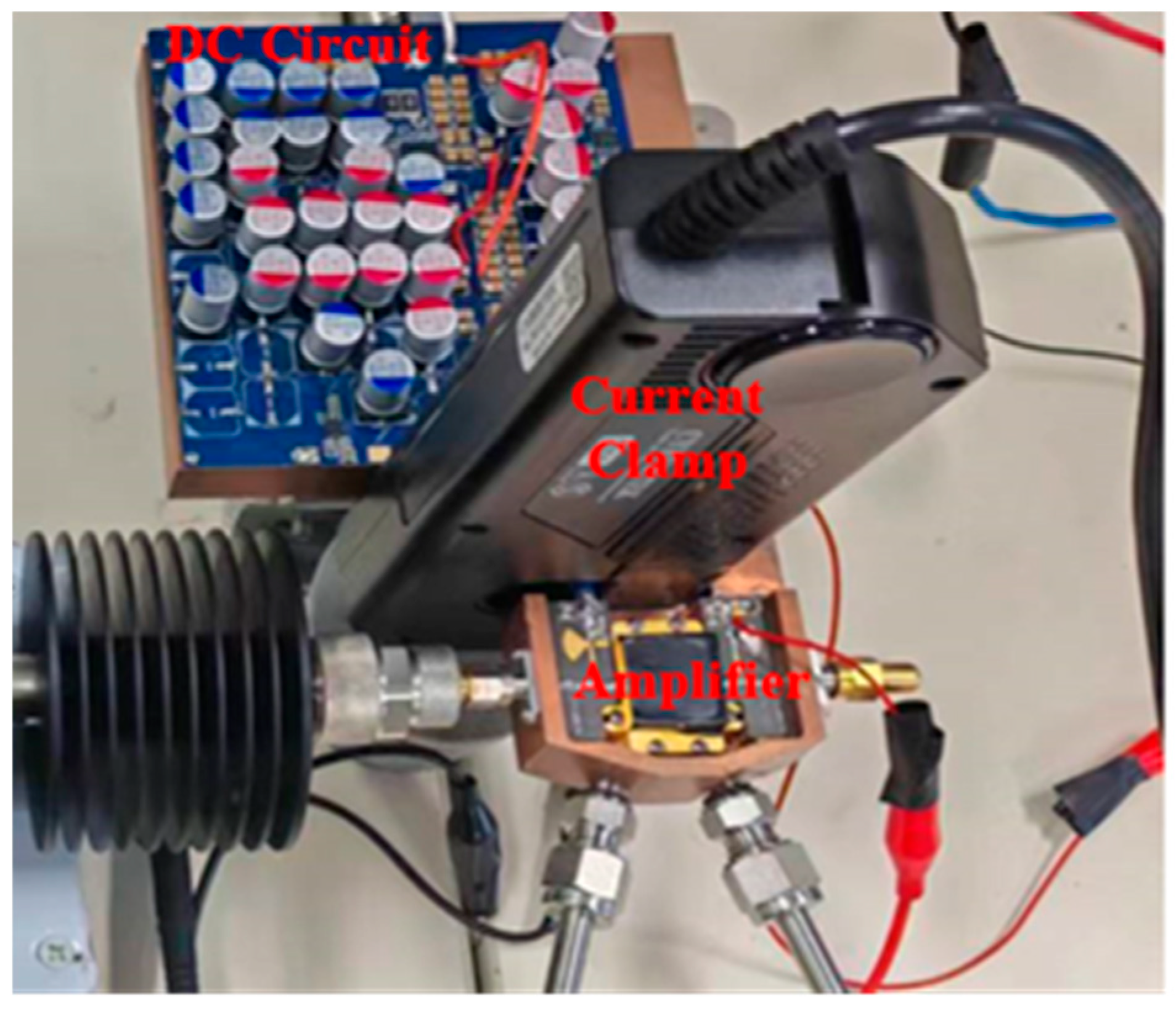
For kW-level pulsed GaN HEMTs, the typical operating pulse width is 5 μs with currents ranging from tens to hundreds of amperes. This measurement used an X-band GaN HEMT to validate the relationship between drain current and temperature [29]. To minimize the drain bias circuit path, a dedicated slot was designed in the test fixture to accommodate the current clamp for drain current measurement. The DC circuit can convert an input continuous voltage signal into a square wave signal, with both the rise time and fall time under 50 ns. Figure 4 illustrates the schematic diagram and physical setup of the drain current waveform measurement.
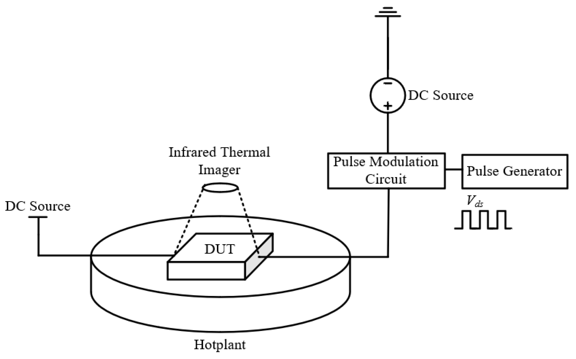
An infrared microscope was used to measure the channel temperature of the power amplifier, and the measurement diagram and infrared detection interface are shown in Figure 5. The infrared detector has a time resolution of the order of μs, so it can only measure the channel temperature change after the initial temperature and the working pulse width of 1 μs [30].

4. Results and Discussion

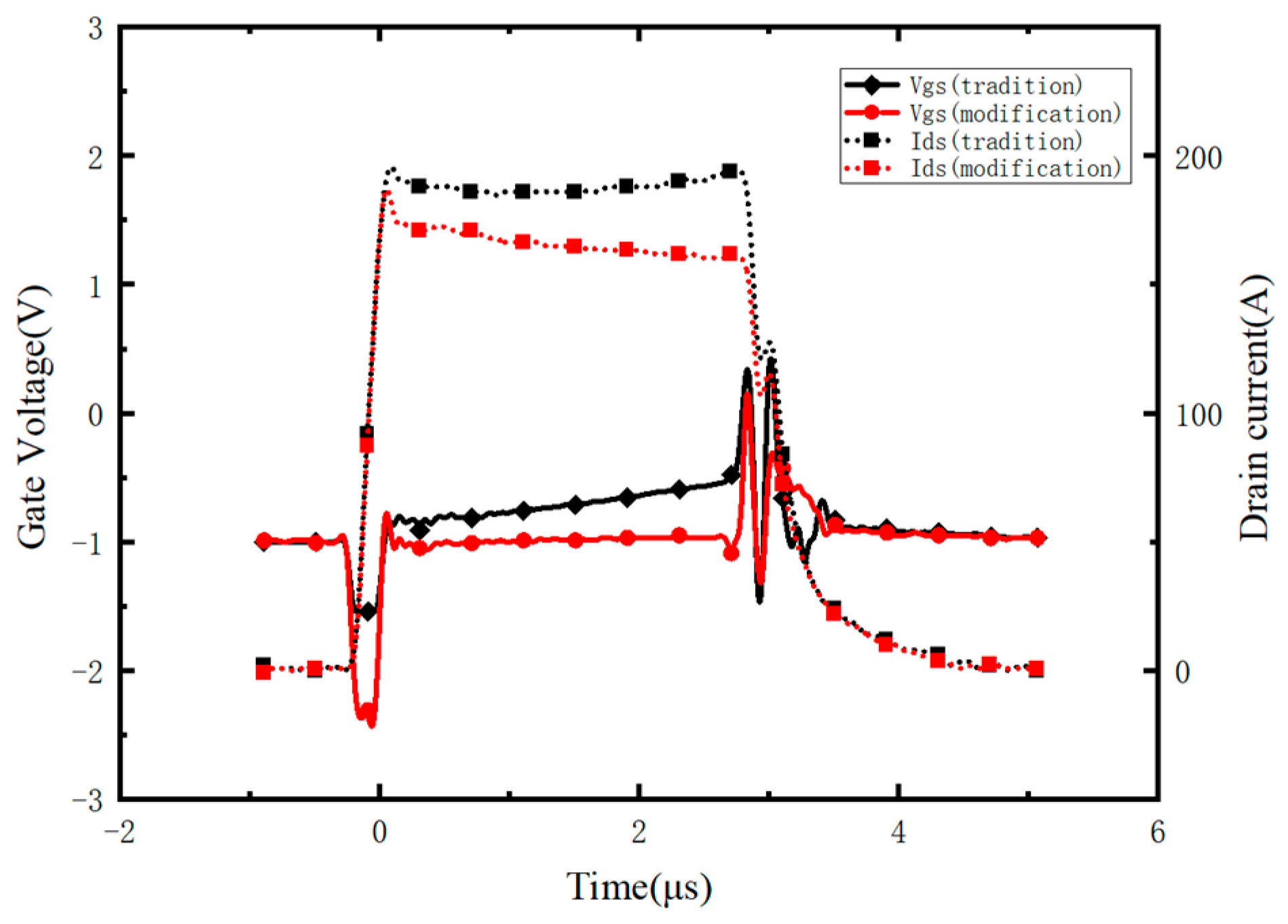
With Vgs set to −1 V and Vds to 60 V, the drain voltage pulse width was configured to 3 μs and the cycle period to 3 ms. The gate voltage and drain current waveforms of the power amplifier were measured at an ambient temperature of 25 °C. The measurement results for both the conventional bias circuit and the optimized practical bias circuit are shown in Figure 6.
The drain current with the conventional bias circuit did not decrease gradually as theoretically expected due to the rising junction temperature during operation. Instead, after an initial decrease, it gradually increased. This behavior is attributed to the gate current slowly rising over time, leading to a corresponding gradual increase in the voltage drop across the bias circuit. Over the 3 μs pulse duration, the gate voltage increased by approximately 0.5 V. The rise in gate voltage resulted in an increase in carrier concentration within the channel, thereby elevating the drain current. Although temperature rise typically causes a reduction in drain current, according to Equation (6), the influence of temperature on drain current diminishes at higher temperatures.
Therefore, during the first half of the pulse width, the decrease in drain current—driven by junction temperature rise and trap effects—dominates the current variation. In the latter half, as trap effects weaken and the temperature’s influence on current variation decreases, the increase in drain current caused by the rising gate voltage becomes the dominant factor. This leads to the observed trend where the current first decreases and then increases.
To ensure that the drain current is solely influenced by temperature variation, it is essential to maintain a constant gate voltage. This study proposes a modified bias circuit that reduces the series gate resistance Rg and adjusts the parallel gate-to-ground capacitance. Under the conditions of Vgs = −1 V, Vds = 60 V, and a drain voltage pulse width of 3 μs, the measured gate voltage is shown in Figure 6. The maximum value recorded during the 3 μs operational pulse was −0.97 V, representing a 94% reduction in gate voltage variation compared to the conventional bias circuit. This modification effectively eliminates the influence of gate voltage fluctuation on the drain current.
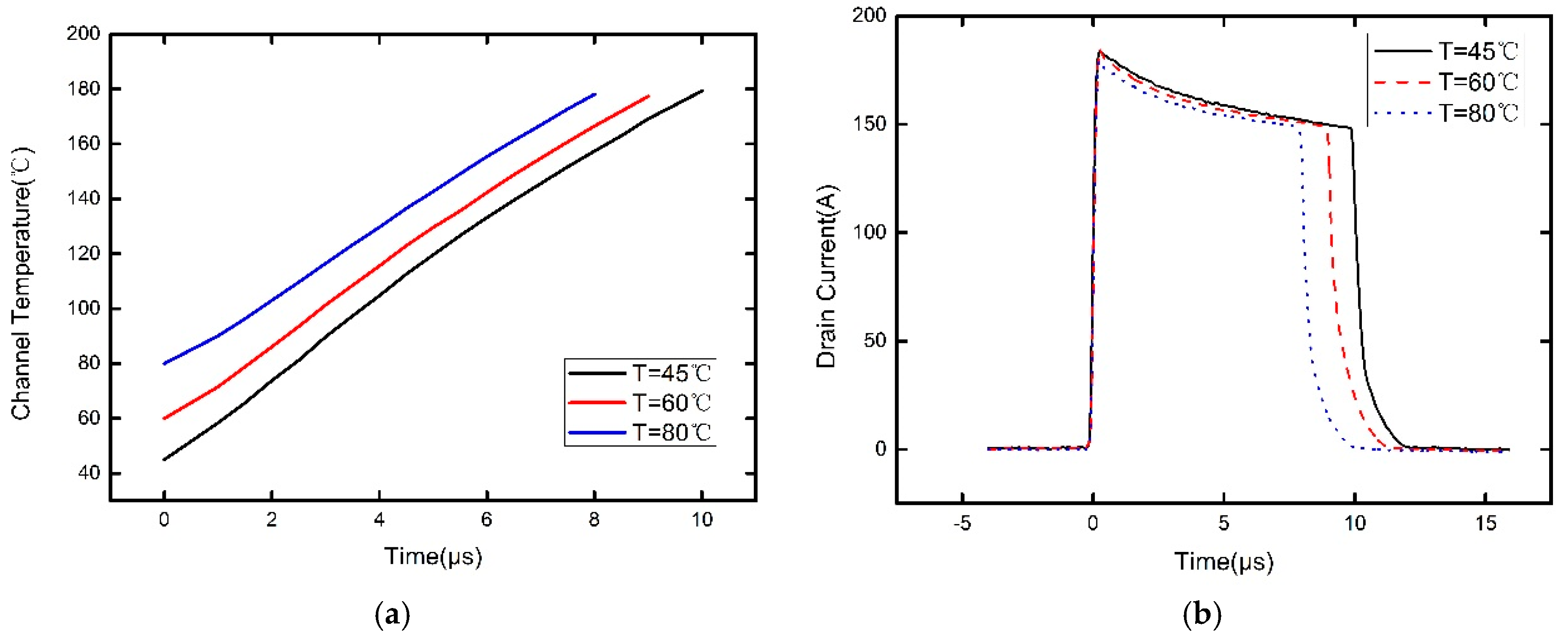
After adjusting the gate bias circuit, we established a measurement system for drain current and channel temperature. Under hotplate temperatures (Thp) of 45 °C, 60 °C, and 80 °C, the drain current curve of the power amplifier was measured using a current clamp, while the temperature profiles of the channel were captured via an infrared thermal imager. The measured curves are shown in Figure 7. The pulse widths used at hotplate temperatures of 45 °C, 60 °C, and 80 °C were 8 μs, 9 μs, and 10 μs, respectively. At these pulse widths, the max channel temperature of the power amplifier is 180 °C, as shown in Figure 7a.
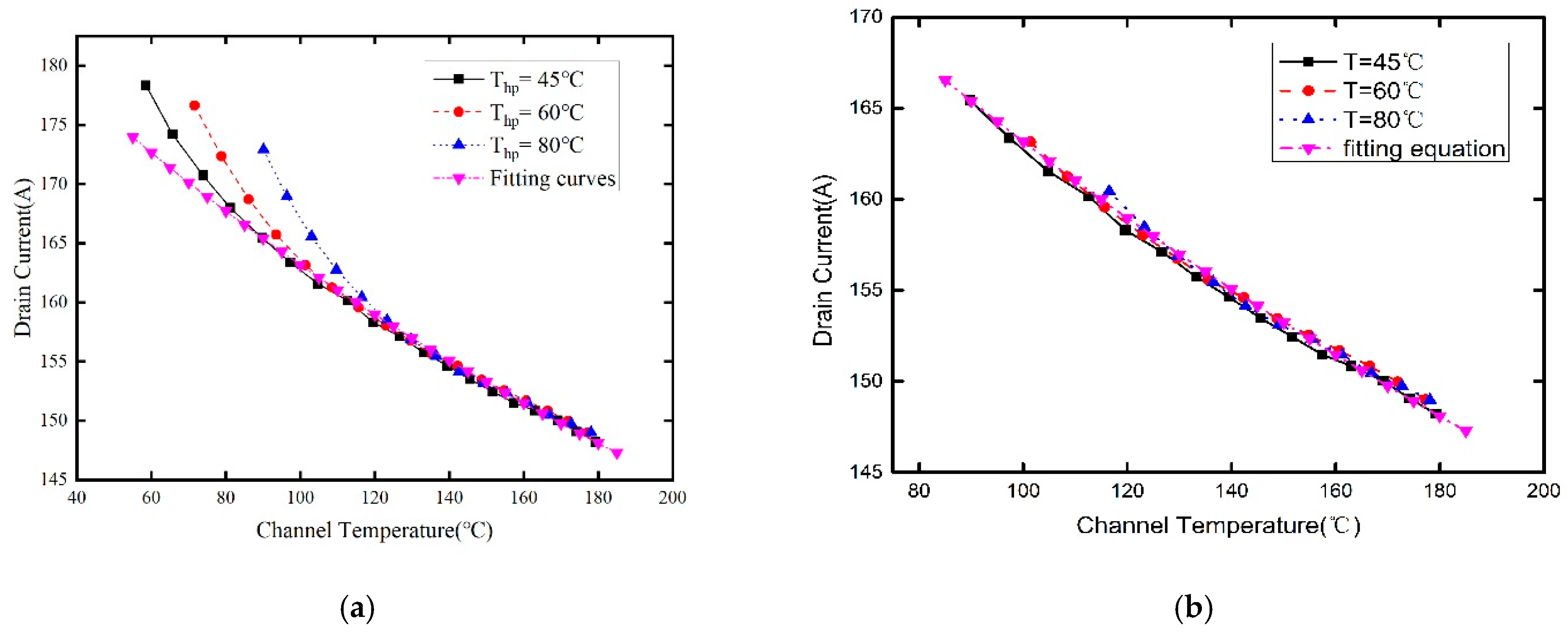
Under a 45 °C hotplate environment, the measured drain current and corresponding channel temperature values were substituted to calculate k = 0.5 in Formula (6). Figure 8a presents the drain current versus channel temperature curves fitted using data measured at the same time point under hotplate temperatures of 45 °C, 60 °C, and 80 °C, along with the fitting curve from Equation (6). Figure 8b shows the drain current versus temperature curves fitted using drain current and channel temperature data taken at the same time point within the 3 μs to 10 μs interval under the same hotplate temperatures, also accompanied by the fitting curve from Equation (6). A comparison between Figure 8a,b indicates a trap time constant of 3 μs, and the extracted 3 microsecond trap time constant is generalizable across measured devices. Within the time range of 3 μs to 10 μs, the relationship between drain current and temperature aligns with the characterization by Equation (6) in Section 2.1, thereby validating the analysis in Section 2.2.2 and Figure 3.
The k-value is independent of ambient temperature. As shown in Figure 8, the drain current remains consistent at a given channel temperature, regardless of the hotplate temperature. However, the k-value is dependent on the drain bias voltage. Therefore, recalibration would be required if a different drain bias voltage is applied or if devices from a different process node are used, in order to accurately determine the k-value.
It is evident that during the initial period after the drain pulse voltage Vds is applied to the HEMT, the internal current is simultaneously influenced by both self-heating effects and trapping effects. For the tested kW-level GaN HEMT, the fitting formula curve represents the magnitude of the current decline due to temperature. In the 0~3 μs timeframe, the trapping effect further accelerates the drain current drop [15]. Beyond this period, the drain current continues to decrease, but the decline is almost exclusively attributed to the self-heating-induced temperature rise in the HEMT. Based on this analysis, the measured current and channel temperature data from the post-3 μs timeframe under different ambient temperatures were selected for fitting, as illustrated in Figure 8. Figure 8 demonstrates that under identical gate and drain voltages, the drain current magnitude is predominantly governed by the channel temperature, as thermal effects alone dominate the current behavior at this stage [20,28,31]. The individual contributions of self-heating and trap trapping are illustrated in Figure 8a. Taking the test results of the 45 °C environmental hot stage as an example, the fitted curve indicates that self-heating accounts for a current reduction of 7 A, meaning that trap trapping is responsible for the remaining 5 A decrease.
By neglecting the impact of trapping effects, the measured current values beyond 3 μs were compared with formula-fitted results. Their absolute and relative errors are shown in Figure 9, which demonstrates an absolute error below 1 A and a relative error less than 0.6%. The experimental results confirm that when the operational pulse width is sufficiently long, the measured drain current under different ambient temperatures is jointly influenced by both trapping effects and self-heating effects within the first 3 μs of the working pulse. Beyond 3 μs, the drain current decline is almost exclusively governed by self-heating effects, with the current magnitude solely dependent on the channel temperature.

5. Conclusions

This paper proposes an electrical thermometry method for measuring the channel temperature of a kW-level GaN HEMT. For high-power GaN HEMTs operating in pulsed mode, the channel temperature directly affects output characteristics such as carrier mobility, drain current, and output power. Furthermore, a higher temperature significantly increases the risk of thermal breakdown and permanent damage to the HEMT. Therefore, monitoring the instantaneous temperature within the pulse is critically important. By modifying the series resistance and parallel-to-ground capacitance in the gate bias circuit, the influence of gate leakage current on gate voltage is minimized to stabilize the gate bias. Based on the derived formula correlating drain current with channel temperature, a comparison with experimental measurements not only yields a trapping time constant of 3 μs but also demonstrates that, under different ambient temperatures, when the duration within the drain voltage pulse exceeds this trapping time constant, the drain current depends solely on channel temperature. By adopting this method, the channel temperature of GaN HEMTs from the same manufacturing process can be tested quickly and accurately after calibration. This effectively solves the problem faced by electrical laboratories that lack microsecond-level optical thermometers, enabling them to measure the transient temperature within pulses.

Author Contributions

Conceptualization, S.Z. and W.F.; methodology, S.Z. and W.H.; software, S.Z.; validation, S.Z., J.Z. and C.F.; formal analysis, S.Z. and L.W.; investigation, S.Z.; resources, W.F.; data curation, T.H.; writing—original draft preparation, S.Z.; writing—review and editing, L.W. and W.F.; visualization, J.Z.; supervision, W.H.; project administration, W.F.; funding acquisition, W.H. All authors have read and agreed to the published version of the manuscript.

Funding

This research received no external funding.

Data Availability Statement

The original contributions presented in this study are included in the article. Further inquiries can be directed to the corresponding author.

Conflicts of Interest

The authors declare no conflicts of interest.

References

  1. Mishra, U.K.; Shen, L.; Kazior, T.E.; Wu, Y.-F. GaN-Based RF Power Devices and Amplifiers. Proc. IEEE 2008, 96, 287–305. [Google Scholar] [CrossRef]
  2. Dunleavy, L.; Baylis, C.; Curtice, W.; Connick, R. Modeling GaN: Powerful but Challenging. IEEE Microw. Mag. 2010, 11, 82–96. [Google Scholar] [CrossRef]
  3. Komiak, J.J. GaN HEMT: Dominant Force in High-Frequency Solid-State Power Amplifiers. IEEE Microw. Mag. 2015, 16, 97–105. [Google Scholar] [CrossRef]
  4. Schwitter, B.K.; Parker, A.E.; Mahon, S.J.; Fattorini, A.P.; Heimlich, M.C. Heimlich Impact of Bias and Device Structure on Gate Junction Temperature in AlGaN/GaN-on-Si HEMTs. IEEE Trans. Electron Devices 2014, 61, 1327–1334. [Google Scholar] [CrossRef]
  5. Zeng, C.; Wang, Y.; Liao, X.; Li, R.; Chen, Y.; Lai, P.; Huang, Y.; En, Y. Reliability assessment of Algangan Hemts for high voltage applications based on high temperature reverse bias test. In Proceedings of the 2014 10th International Conference on Reliability, Maintainability and Safety (ICRMS), Guangzhou, China, 6–8 August 2014; pp. 298–301. [Google Scholar] [CrossRef]
  6. Park, J.; Shin, M.W.; Lee, C.C. Thermal modeling and measurement of AlGaN-GaN HFETs built on sapphire and SiC substrates. IEEE Trans. Electron Devices 2004, 51, 1753–1759. [Google Scholar] [CrossRef]
  7. Killat, N.; Montes, M.; Pomeroy, J.W.; Paskova, T.; Evans, K.R.; Leach, J.; Li, X.; Ozgur, U.; Morkoc, H.; Chabak, K.D.; et al. Thermal Properties of AlGaN/GaN HFETs on Bulk GaN Substrates. IEEE Electron Device Lett. 2012, 33, 366–368. [Google Scholar] [CrossRef]
  8. Prejs, A.; Wood, S.; Pengelly, R.; Pribble, W. Thermal analysis and its application to high power GaN HEMT amplifiers. In Proceedings of the 2009 IEEE MTT-S International Microwave Symposium Digest, Boston, MA, USA, 7–12 June 2009; pp. 917–920. [Google Scholar] [CrossRef]
  9. Harris, M.; Wagner, B.; Tong, W.; Menkara, H.; Halpern, S. Thermal analysis and validation of packaging for 100W and higher GaN MMIC power amplifiers. In Proceedings of the WAMICON 2011 Conference Proceedings, Clearwater Beach, FL, USA, 18–19 April 2011; pp. 1–5. [Google Scholar] [CrossRef]
  10. Shen, Y.; Chen, X.-S.; Hua, Y.-C.; Li, H.-L.; Wei, L.; Cao, B.-Y. Bias Dependence of Non-Fourier Heat Spreading in GaN HEMTs. IEEE Trans. Electron Devices 2023, 70, 409–417. [Google Scholar] [CrossRef]
  11. Hu, Z.; Gao, X.; Cai, S. Electro-thermal model extraction of power GaN HEMT using I–V pulsed and DC measurements. In Proceedings of the 2011 9th IEEE International Conference on ASIC, Xiamen, China, 25–28 October 2011; pp. 850–853. [Google Scholar] [CrossRef]
  12. McAlister, S.P.; Bardwell, J.A.; Haffouz, S.; Tang, H. Self-heating and the temperature dependence of the DC characteristics of GaN heterostructure field effect transistors. J. Vac. Sci. Technol. A 2006, 24, 624–628. [Google Scholar] [CrossRef]
  13. Simms, R.J.T.; Pomeroy, J.W.; Uren, M.J.; Martin, T.; Kuball, M. Channel Temperature Determination in High-Power AlGaN/GaN HFETs Using Electrical Methods and Raman Spectroscopy. IEEE Trans. Electron Devices 2008, 55, 478–482. [Google Scholar] [CrossRef]
  14. Kuzmik, J.; Javorka, R.; Alam, A.; Marso, M.; Heuken, M.; Kordos, P. Determination of channel temperature in AlGaN/GaN HEMTs grown on sapphire and silicon substrates using DC characterization method. IEEE Trans. Electron Devices 2002, 49, 1496–1498. [Google Scholar] [CrossRef]
  15. Santarelli, A.; Di Giacomo, V.; Cignani, R.; D’Angelo, S.; Niessen, D.; Filicori, F. Nonlinear thermal resistance characterization for compact electrothermal GaN HEMT modelling. In Proceedings of the 5th European Microwave Integrated Circuits Conference, Paris, France, 27–28 September 2010; pp. 82–85. [Google Scholar]
  16. Dahmani, S.; Mengistu, E.S.; Kompa, G. Thermal Model Extraction of GaN HEMTs for Large-Signal Modeling. In Proceedings of the 2008 European Microwave Integrated Circuit Conference, Amsterdam, The Netherlands, 27–28 October 2008; pp. 226–229. [Google Scholar] [CrossRef]
  17. Rashmi; Kranti, A.; Haldar, S.; Gupta, M.; Gupta, R.S. Comprehensive analysis of small-signal parameters of fully strained and partially relaxed high Al-content lattice mismatched Al/sub m/Ga/sub 1-m/N/GaN HEMTs. IEEE Trans. Microw. Theory Tech. 2003, 51, 607–617. [Google Scholar] [CrossRef]
  18. Rashmi; Kranti, A.; Haldar, S.; Gupta, R.S. An accurate charge control model for spontaneous and piezoelectric polarization dependent two-dimensional electron gas sheet charge density of lattice-mismatched AlGaN/GaN HEMTs. Solid-State Electron. 2002, 46, 621–630. [Google Scholar] [CrossRef]
  19. Wei, J.; Xu, H.; Xie, R.; Chen, K.J. Principles and impacts of dynamic threshold voltage in a p-GaN gate high-electron-mobility transistor. Semicond. Sci. Technol. 2018, 36, 024006. [Google Scholar] [CrossRef]
  20. Tsividis, Y.; McAndrew, C. Operation and Modeling of the MOS Transistor, 3rd ed.; Oxford University Press: New York, NY, USA, 2011; pp. 181–194. [Google Scholar]
  21. Anghel, C.; Gillon, R.; Ionescu, A.M. Self-heating characterization and extraction method for thermal resistance and capacitance in HV MOSFETs. IEEE Electron Device Lett. 2004, 25, 141–143. [Google Scholar] [CrossRef]
  22. Joh, J.; del Alamo, J.A.; Chowdhury, U.; Chou, T.-M.; Tserng, H.-Q.; Jimenez, J.L. Measurement of Channel Temperature in GaN High-Electron Mobility Transistors. IEEE Trans. Electron Devices 2009, 56, 2895–2901. [Google Scholar] [CrossRef]
  23. Florian, C.; Santarelli, A.; Cignani, R.; Filicori, F. Characterization of the Nonlinear Thermal Resistance and Pulsed Thermal Dynamic Behavior of AlGaN–GaN HEMTs on SiC. IEEE Trans. Microw. Theory Tech. 2013, 61, 1879–1891. [Google Scholar] [CrossRef]
  24. Kang, T.-S.; Ren, F.; Gila, B.P.; Pearton, S.J.; Patrick, E.; Cheney, D.J.; Law, M.; Zhang, M.-L. Investigation of traps in AlGaN/GaN high electron mobility transistors by sub-bandgap optical pumping. J. Vac. Sci. Technol. B Nanotechnol. Microelectron. 2015, 33, 061202. [Google Scholar] [CrossRef]
  25. Ahmed, N.; Dutta, A.K. Analytical models for the 2DEG concentration and gate leakage current in AlGaN/GaN HEMTs. Solid-State Electron. 2017, 132, 64–72. [Google Scholar] [CrossRef]
  26. Gao, L.; Zhong, Z.; Zhang, Q.; Li, X.; Xiong, X.; Chen, S.; Chen, L.; Yan, H.; Zhang, A.; Han, J.; et al. Stability of GaN HEMT Device Under Static and Dynamic Gate Stress. IEEE J. Electron Devices Soc. 2024, 12, 165–169. [Google Scholar] [CrossRef]
  27. Santarelli, A.; Cignani, R.; Niessen, D.; Traverso, P.A.; Filicori, F. New pulsed measurement setup for GaN and GaAs FETs characteri zation. Int. J. Microw. Wirel. Technol. 2012, 4, 387–397. [Google Scholar] [CrossRef]
  28. Gomes, J.L.; Nunes, L.C.; Gonçalves, C.F.; Pedro, J.C. An Accurate Characterization of Capture Time Constants in GaN HEMTs. IEEE Trans. Microw. Theory Tech. 2019, 67, 2465–2474. [Google Scholar] [CrossRef]
  29. Stockman, A.; Masin, F.; Meneghini, M.; Zanoni, E.; Meneghesso, G.; Bakeroot, B.; Moens, P. Gate Conduction Mechanisms and Lifetime Modeling of p-Gate AlGaN/GaN High-Electron-Mobility Transistors. IEEE Trans. Electron Devices 2018, 65, 5365–5372. [Google Scholar] [CrossRef]
  30. Sun, Y.; Wang, M.; Lei, W.; Han, C. Dynamic gate leakage current of p-GaN Gate AlGaN/GaN HEMT under positive bias Conditions. In Proceedings of the 2021 IEEE Workshop on Wide Bandgap Power Devices and Applications in Asia (WiPDA Asia), Wuhan, China, 25–27 August 2021; pp. 232–235. [Google Scholar] [CrossRef]
  31. Jardel, O.; De Groote, F.; Reveyrand, T.; Jacquet, J.-C.; Charbonniaud, C.; Teyssier, J.-P.; Floriot, D.; Quere, R. An Electrothermal Model for AlGaN/GaN Power HEMTs Including Trapping Effects to Improve Large-Signal Simulation Results on High VSWR. IEEE Trans. Microw. Theory Tech. 2007, 55, 2660–2669. [Google Scholar] [CrossRef]
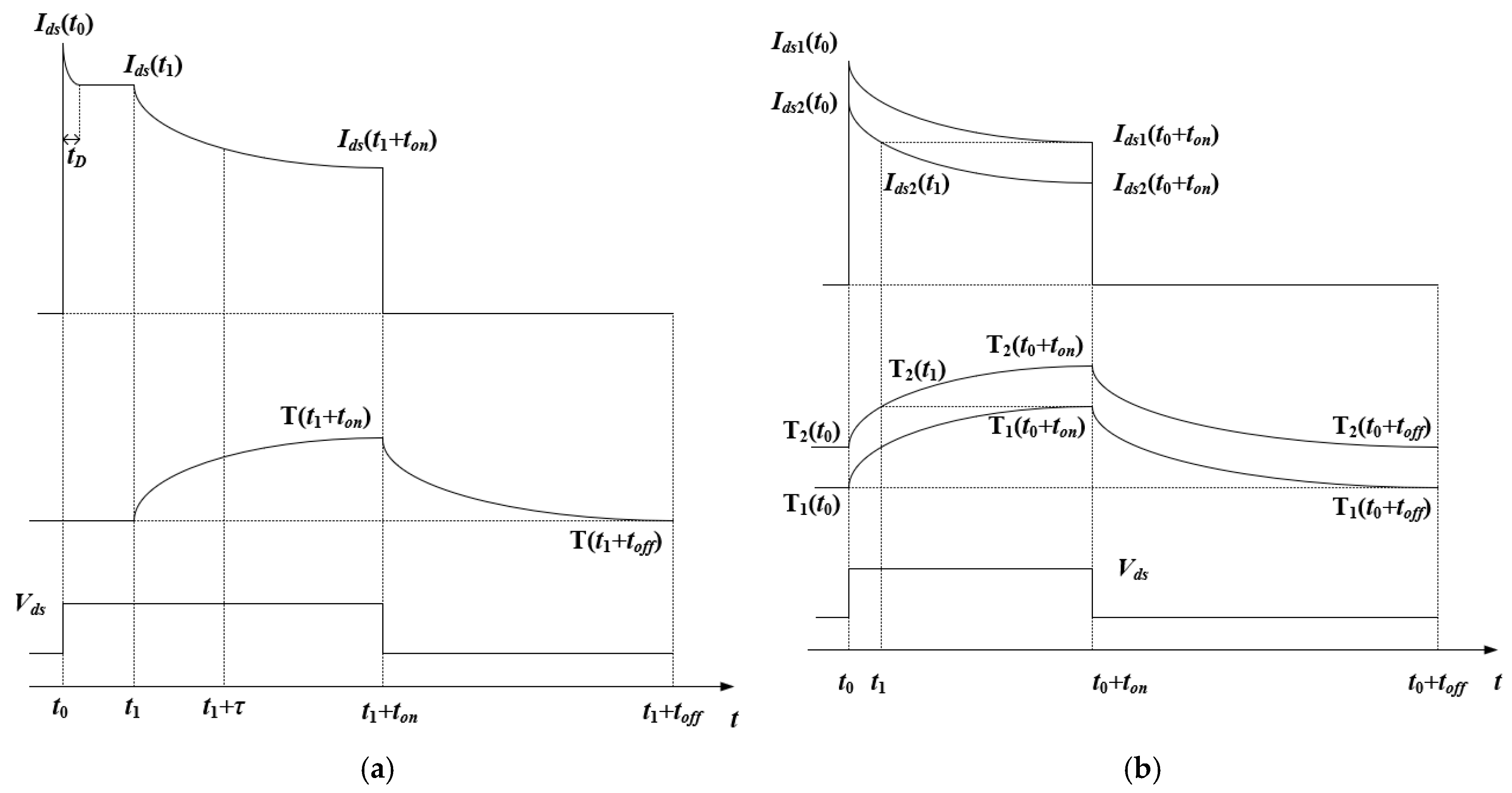
Figure 1. (a) Drain current and channel temperature waveforms corresponding to a drain voltage pulse. (b) Time-domain waveforms of the drain current and channel temperature corresponding to the same drain voltage pulse and different ambient temperatures.
Electronics 14 03861 g001
Figure 2. (a) Traditional gate bias circuit. (b) The proposed gate bias circuit.
Electronics 14 03861 g002
Figure 3. Measured S-parameters of the traditional gate bias circuit and the proposed gate bias circuit.
Electronics 14 03861 g003
Figure 4. Drain current waveform measurement system.
Electronics 14 03861 g004
Figure 5. Schematic diagram of infrared temperature measurement.
Electronics 14 03861 g005
Figure 6. Drain current and gate voltage waveforms under traditional measurement condition and modified grid circuit condition.
Electronics 14 03861 g006
Figure 7. Comparison of the channel temperature waveform (a) and the drain current waveform (b) under different hotplate temperatures.
Electronics 14 03861 g007
Figure 8. Temperature-dependent variation curves of all time (a) and post-3 μs (b) drain current and formula-fitted current values under different hotplate temperatures.
Electronics 14 03861 g008
Figure 9. Absolute error and relative error between the measured post-3 μs drain current and the formula-fitted results.
Electronics 14 03861 g009
Disclaimer/Publisher’s Note: The statements, opinions and data contained in all publications are solely those of the individual author(s) and contributor(s) and not of MDPI and/or the editor(s). MDPI and/or the editor(s) disclaim responsibility for any injury to people or property resulting from any ideas, methods, instructions or products referred to in the content.