1. Introduction
Advancements in CMOS process technologies have driven the widespread development of K-band receivers and Ka-band transmitters for LEO SATCOM user terminals, as well as Ka-band CMOS phased-array transceivers for 5G applications in the 26.5–29.5 GHz and 37–40 GHz bands [
1,
2,
3,
4]. In a Ka-band transmitter for LEO SATCOM UTs, a CMOS four-way power splitter plays a critical role by aggregating the output power (P
out) from four CMOS power amplifiers (PAs) to deliver approximately 22 dBm, which is sufficient to drive a GaN PA. This allows the GaN PA to deliver an output power with 1-dB compression (OP
1dB) of around 39 dBm, supporting normal operation at a P
out of 33 dBm with a 6-dB power back-off (PBO), as described in the following section. Similarly, in a 5G phased-array transceiver, a CMOS four-way power splitter is equally essential. It either splits the modulated baseband signal into four RF paths or combines the signals from these paths, depending on the operation mode. The functionality will also be detailed in the next section.
In addition to a compact chip size, the fundamental requirements for a four-way power splitter include low input and output return loss (S
11 and S
22 better than −10 dB), low transmission loss (S
21 to S
51 greater than −8.2 dB), high isolation between output ports (better than −15 dB), low amplitude inequality (AI) magnitude (AIM < 0.1 dB), and low phase deviation (PD) magnitude (PDM < 1°). The power splitters proposed in this work meet all of these criteria, as will be detailed in
Section 6. To date, various two-way and four-way power splitters operating at microwave and millimeter-wave frequencies have been demonstrated [
5,
6,
7,
8,
9,
10,
11]. However, many of these designs still suffer from performance limitations. For example, the 24 GHz 4-way lumped-element power splitter reported in [
6] employs four equivalent quarter-wavelength (λ/4) transmission lines (TLs) and four 50 Ω resistors, achieving a small chip size of 0.109 mm
2. Despite this, the design suffers from relatively high transmission loss (S
21–S
51 ≈ −8 to −8.1 dB at 24 GHz) and a limited input-matching bandwidth at port 1 (S
11 bandwidth of 35.9%, from 19.4 to 27.9 GHz). These shortcomings are attributed in part to the use of an octagonal helical TL layout. In [
7], the 32 GHz 4-way differential power splitter consists of multi-section coupled inductors. Decent transmission loss of −7.85~−7.95 dB at 32 GHz is attained. However, the chip size of 0.144 mm
2 and the S
11 bandwidth of 29.6% (24.5–33 GHz) still leave room for improvement, in part due to the use of a square-helical TL layout. To decrease chip size and enhance performance, three CMOS four-way power splitter designs incorporating RC isolation networks are proposed and analyzed in this work. The first power splitter (PS1) consists of a two-way power splitter using circular double-helical (DH) TLs cascaded with two two-way power splitters using noninverting circular sole-helical coupled-TL (SH-CL). The second power splitter (PS2) consists of a two-way power splitter using circular DH-TLs cascaded with two two-way power splitters using inverting circular SH-CL. The third power splitter (PS3) consists of three two-way power splitters using circular DH-TLs. The novelty is as follows. First, a parallel capacitor C
1 at the input of each two-way power splitter to satisfy the requirement for two equivalent quarter-wavelength (λ/4) TLs, ensuring a low input reflection coefficient. A parallel R
p2C
p2 (or R
p3C
p3) isolation network is connected between the outputs of each two-way power splitter to attain decent reflection coefficients and isolation. Compact chip size and low insertion loss are attained in PS1 due to the utilization of a lumped-distributed noninverting sole-helical topology with a TL physical length of λ/12. Similarly, PS2 achieves compact chip size and low insertion loss through a lumped-distributed inverting sole-helical topology with a TL physical length of λ/9. Second, PS1, which uses noninverting two-way power splitters, attains nearly impeccable AI and PD thanks to its careful layout. PS2, using inverted two-way power splitters, also attains nearly impeccable AI and PD due to its symmetrical layout. Note that the transmission loss (S
21-S
51) of a millimeter-wave four-way power splitter is influenced by substrate resistivity and the backend-of-line (BEOL) process. While this work uses 0.18 μm CMOS technology, the transmission loss could be further reduced by adopting a more advanced technology, such as the 22 nm FD-SOI CMOS process with high substrate resistivity and ultra-thick metal layers, as demonstrated in [
9]. The remainder of the paper is organized as follows:
Section 2 introduces the theory of the four-way power splitters;
Section 3 describes the design of the four-way power splitters; simulation results are presented in
Section 4;
Section 5 discusses measurement results and compares them with previous work; and, finally,
Section 6 presents the conclusion.
2. K/Ka-Band LEO SATCOM and 5G Radio Systems
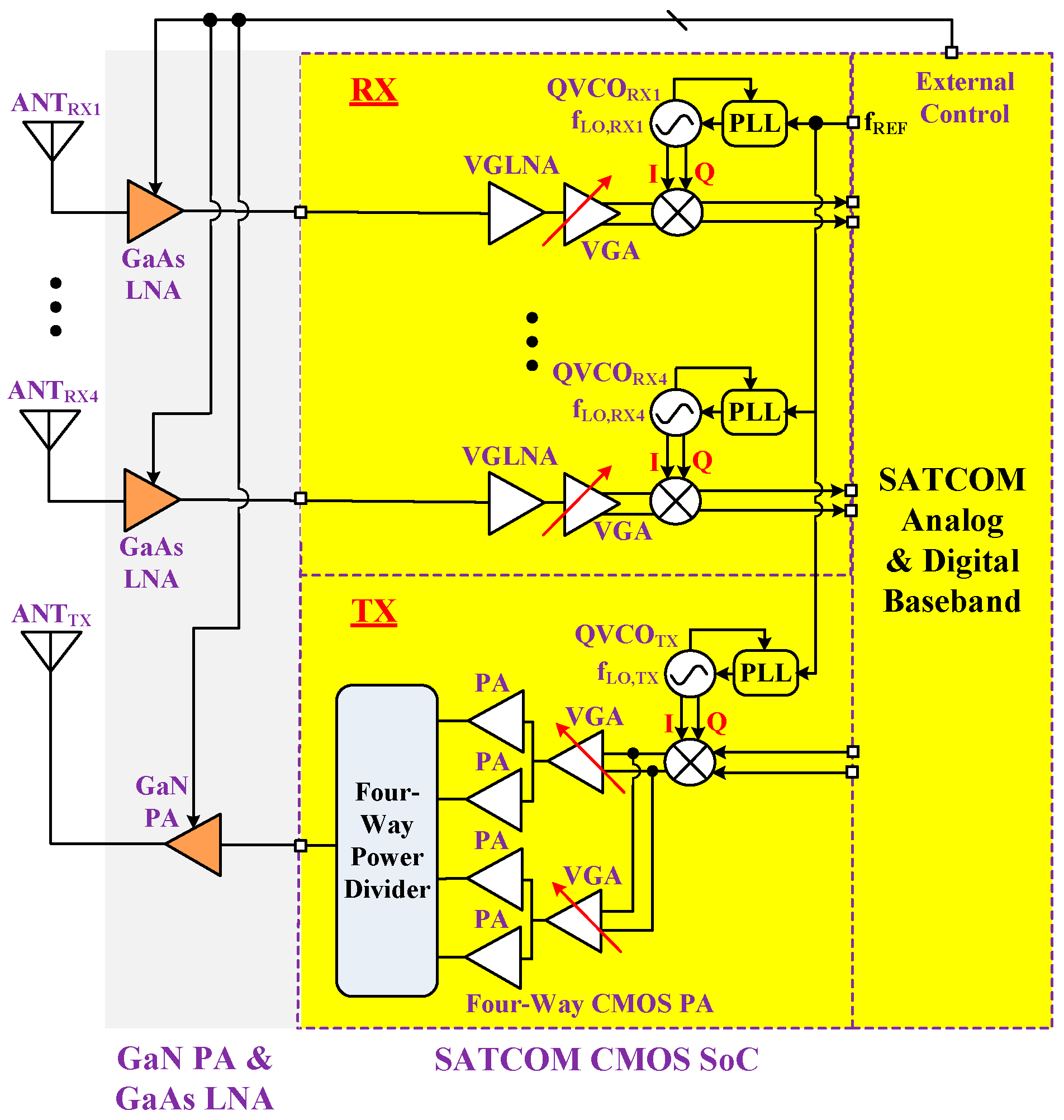
Figure 1 illustrates the proposed K/Ka-band CMOS–GaN/GaAs hetero-integrated transceiver front-end architecture for LEO SATCOM UTs. This represents a pioneering design approach for achieving a low-power, low-noise, high-gain, and high-sensitivity compact K-band CMOS–GaAs hetero-integrated receiver front-end (four channels in this example), and a high-P
out, high-linearity, and high-efficiency compact Ka-band CMOS–GaN hetero-integrated transmitter front-end (with four CMOS power amplifiers (PAs) operating in parallel). Each channel of the K-band receiver front-end consists of a GaAs LNA, cascaded with a CMOS VGLNA, a VGA, and a down-conversion mixer. Typical specifications for a K-band receiver targeting LEO SATCOM UTs include a variable gain of 20–60 dB, an NF ranging from 1.35 to 4 dB, and an input power with 1-dB compression (IP
1dB) between −60 and −30 dBm over the 17–21 GHz frequency range. The Ka-band transmitter front-end comprises a CMOS up-conversion mixer, two CMOS VGAs, four CMOS PAs, a CMOS four-way power splitter, and a GaN PA. The CMOS four-way power splitter plays a critical role by merging the output power from the four CMOS PAs to achieve approximately 22 dBm, which is sufficient to drive the GaN PA. The GaN PA, in turn, delivers the required output power with 1-dB compression (OP
1dB) of approximately 39 dBm, enabling normal operation at a P
out of 33 dBm with a 6 dB PBO. Typical specifications for the Ka-band transmitter include a gain of 60 dB, an NF of 10.1 dB, and OP
1dB of 39 dBm over the 28–32 GHz frequency range. Under operating conditions, where the UT transmits at 2 W (33 dBm) and the LEO satellite transmits at 5 W (37 dBm), both the uplink and downlink carrier-to-noise power density ratio (CNR) reach 115 dB·Hz. This supports 256-APSK modulation at a symbol rate of 350 MS/s, fully compliant with DVB-S2X SATCOM standards.
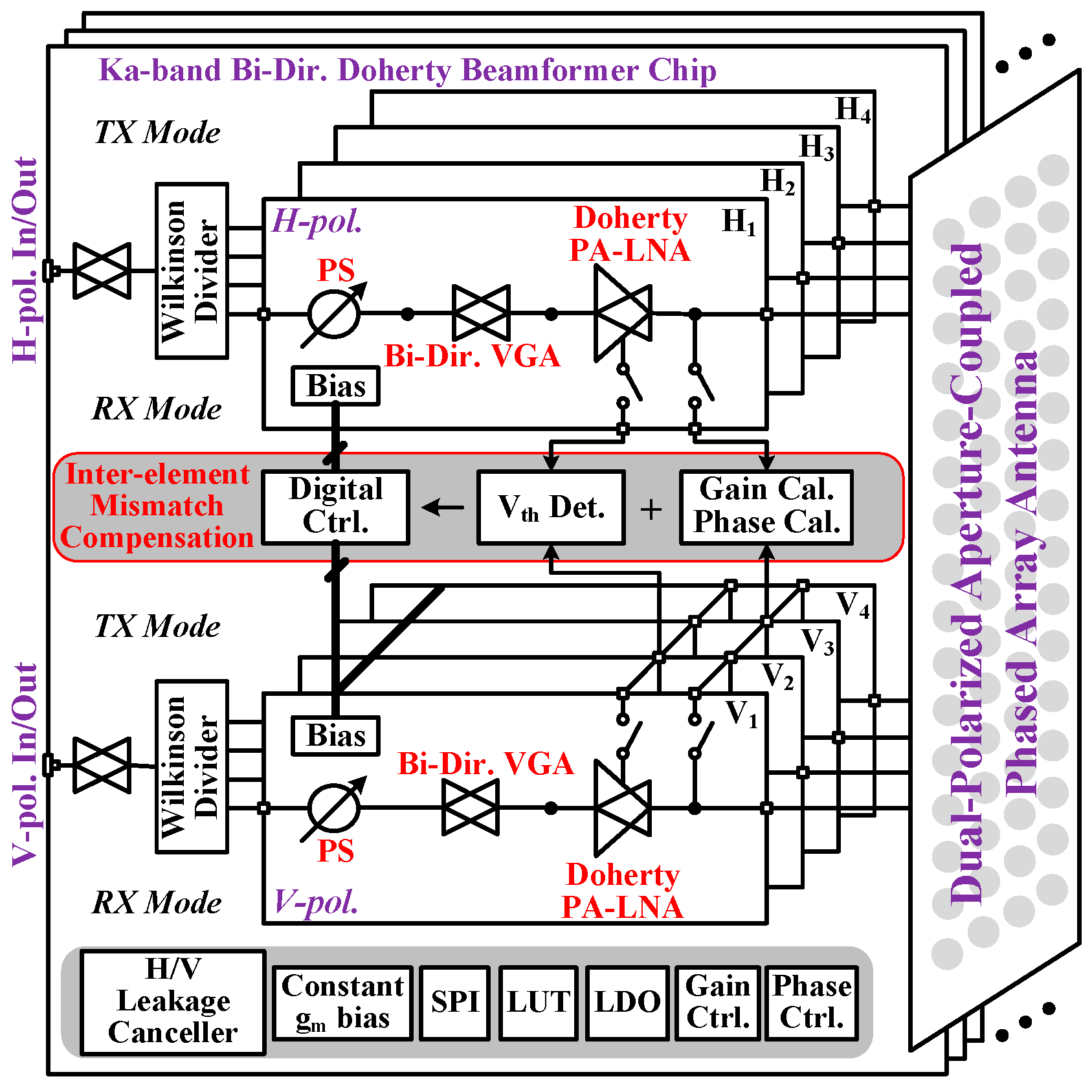
Figure 2 presents an illustration of a Ka-band bidirectional transceiver IC unit featuring four channels and double polarization. The unit is designed to operate over the 26.5–29.5 GHz and 37–40 GHz frequency ranges for 5G communications. In a 16×4 phased-array transceiver, each of the four digital channels incorporates four such IC units. Each IC unit contains eight beamforming paths, with four paths dedicated to horizontal (H) polarization and the other four to vertical (V) polarization. Each path consists of a bidirectional PA–LNA, a bidirectional VGA, and a phase shifter. As shown in
Figure 2, a critical component in this architecture is the bidirectional four-way power splitter/combiner, which performs two primary functions: (1) during transmission, it divides the modulated baseband signal into four RF paths (H1–H4 or V1–V4); (2) during reception, it combines the received RF signals from those same paths. The proposed power splitters, featuring compact and symmetrical layouts, attain an AIM of less than 0.1 dB and a PDM of less than 1° across 26.5–40 GHz, as will be detailed in the following sections. This high level of balance ensures that beamforming can be accurately controlled by adjusting the phase shifters in each path—without the need for additional calibration. Furthermore, compared to the conventional 37–40 GHz 64-element transceiver architecture reported in [
2]—which requires built-in phase and amplitude calibration as well as LO-feedthrough (LOFT) correction for 5G radio in 65 nm CMOS—the proposed bidirectional transceiver topology offers significant advantages. These include a simpler circuit and system architecture, smaller chip size, and ultimately, lower implementation cost.
In addition to achieving a chip size smaller than 0.01 mm2, the three power splitters presented in this work meet key performance requirements across 26.5–40 GHz: input/output reflection coefficients (S11–S55) lower than −10 dB, transmission loss (S21–S51) better than −8.2 dB, output isolation better than −15 dB, AIM less than 0.1 dB, and PDM less than 1°. These metrics confirm that the power splitters are suitable for both 28–32 GHz Ka-band LEO SATCOM transmitters and 26.5–29.5/37–40 GHz Ka-band 5G radio systems.
3. Four-Way Power Splitter Theory
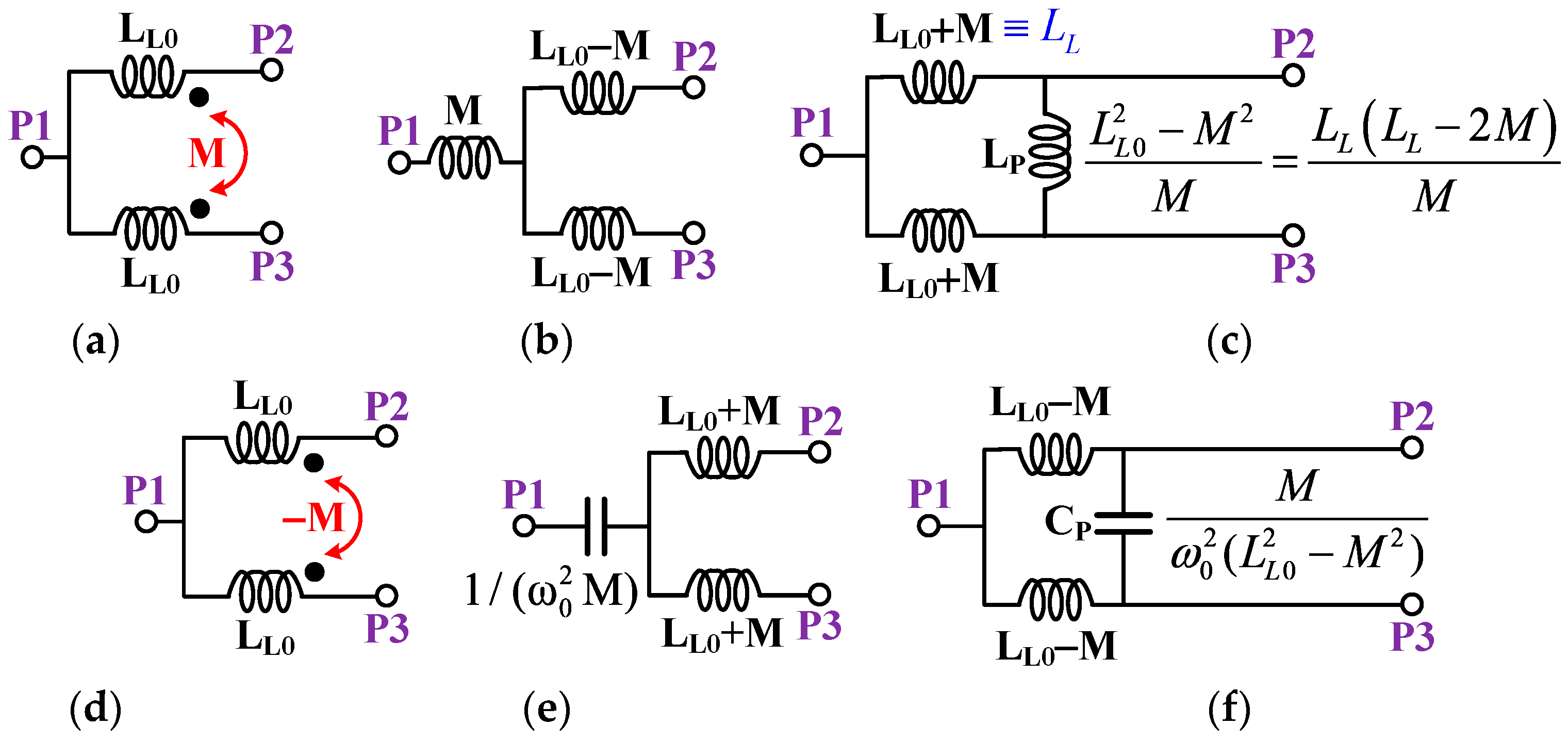
Figure 3a–c presents the small-signal models of a noninverting coupled TLs (CL) in normal, starlike (that is, Y), and triangle (that is, Δ) topologies. The noninverting helical CL has a non-negative mutual inductance in Δ topology (see
Figure 3c). For double-λ/4-TL-based devices, like the two-way power splitter and sole-pole double-throw (SPDT) switch, the needed double λ/4 TLs can be substituted by a miniature noninverting sole-helical CL. The advantages are TL-length decrease (from λ/4 to λ/12) and transmission loss and linearity enhancement.
Figure 3d–f presents the small-signal models of inverting CLs in normal, Y, and Δ topologies. The inverting helical-CL has positive mutual inductance in Y configuration. For double-λ/4-TL-based devices, the required two λ/4 TLs can be substituted by a symmetrical and compact inverting sole-helical CL. The advantages are TL-length reduction (from λ/4 to λ/9) and transmission loss and linearity enhancement. In this work, we present three Ka-band compact and wideband four-way power splitters (PS1-PS3), which are based on circular DH-TLs, and noninverting and inverting SH-CL.
For λ/4-TL-based devices, the λ/4-TL (with characteristic impedance (Z
TL) of Z
TL0) can be substituted by an equivalent lumped-distributed structure for compact size.
Figure 4a presents the illustrative figure and model of the lumped-distributed two-way power splitter. It has a shunt capacitor C
1 at the input for better impedance matching and a shunt RC (that is, R
p1C
p1) between the two outputs for better isolation [
9]. Theoretically, the electrical length (
θ) of the TLs may assume any value within the range of 0° to 90°. For a TL with a θ of θ
1, the corresponding values of Z
TL1 and C
p1 are determined as follows:
The center frequency, f
0, is defined as ω
0/2π. Furthermore, each TL in the two-way lumped-distributed power splitter described in [
10] incorporates an additional end capacitance, denoted as C
pa. For a TL with a θ of θ
2, the required values of Z
TL2 and C
pa are determined as follows:
The reliance on supplementary end capacitance renders the power splitter configuration in [
10] generally less advantageous.
Figure 4b presents the illustrative figure and model of the noninverting SH-CL-based two-way power splitter. It can largely reduce the needed chip size. Compared to the power splitter shown in
Figure 4a, the topology exhibits the same equivalent circuit at ω
0. The key difference lies in the use of two noninverting TLs with magnetic coupling, which introduces a positive mutual inductance, denoted by M. This mutual coupling results in a reduction in the required θ of the TLs. Based on the Y-Δ transformation, the magnetically coupled TLs can be represented in the Δ configuration as two series inductance L
L (
) and a shunt inductance L
P (=L
L(L
L−2M)/M). L
L represents the sum of the self-inductance L
L0 (
) and the mutual inductance M (
) of the helical TLs. θ
0 (36°, equivalent to λ/10 in this article) represents the effective θ of each helical TL when mutual coupling is absent. This corresponds to a physical θ of 30° (approximately λ/12) per helical TL. Near ω
0, L
P becomes negligible, as it resonates in parallel with C
pr. As an example, consider the Ka-band noninverting sole-helical two-way power splitter in PS1 (will be detailed later). In this case, Z
TL1 is 88.9 Ω.
The needed θ of the TL is 30° (i.e., λ/12). Compared to the straight distributed power splitter, this corresponds to a 30.1% reduction in the needed TL length. From
Figure 4b, the corresponding values of L
L0, M, coupling factor k (=M/L
L0), L
P, and C
pr are 0.28 nH, 0.012 nH, 0.04, 6.51 nH, and 3.6 fF, respectively. C
1 (=2C
p1) is 58.4 fF. C
p2 (=C
p1 + C
p) is 32.8 fF. Theoretically, the parasitic series resistance of the two noninverting TLs with magnetic coupling generates a resistance of R
p in parallel with L
P. The needed R
p2 (=
) is thus determined accordingly. In this work, R
p is 379.3 Ω and R
p1 is 100 Ω, which results in a required R
p2 of 135.8 Ω. With careful layout optimization, the parasitic R
p can be approximately 100 Ω, making the inclusion of R
p2 unnecessary. This, in turn, allows for a further reduction in chip size.
Figure 4c presents an illustration of the inverting sole-helical-CL-based two-way power splitter, which offers a significant reduction in the required chip size. Compared to the noninverting structure in
Figure 4b, the design allows for a symmetrical sole-helical layout (will be detailed later). The primary differences lie in the expressions for R
p and C
p within the parallel RC isolation network, and notably, the absence of the L
P term. The two inverting TLs exhibit a negative mutual inductance of −M in the Δ-configuration (refer to
Figure 3f), which results in a slight increase in the required θ for a given TL inductance. Nevertheless, the power splitter attains a substantial reduction in TL-length—from λ/4 to λ/9—as well as improvements in AI and PD, attributable to the symmetrical and helical lumped-distributed structure. Based on the Y-Δ transformation, the coupled TLs can be represented in Δ–equivalent form as two series inductance L
L (=
) and one capacitance C
P (=M/(ω
02L
L(L
L + 2M))) (see
Figure 3f). Here, L
L is the sum of the self-inductance L
L0 (=
) and the negative mutual inductance −M (=
) of the helical TLs. The equivalent electrical length θ
0 (60°, i.e., λ/6 in this article), corresponding to a physical length of 41.5° (approximately λ/9) per helical TL when mutual coupling is absent. C
P can be considered a portion of the required capacitance in the R
p1C
p1 isolation network under the condition of no mutual coupling. As a result, the required C
p3 becomes C
p1−C
P. With a carefully optimized layout, the parasitic C
P can approach the value of C
p1, making C
p1 unnecessary and enabling further layout size reduction. As an example, consider the Ka-band inverting sole-helical two-way power splitter in PS2 (will be detailed later). For this design, Z
TL1 is 79.5 Ω, and the required electrical length of the helical TLs is 54°. This corresponds to a 23.1% reduction in TL length compared to a straight distributed power splitter. For the two inverting two-way power splitters in PS2, the values of L
L0, M, coupling factor k (=M/L
L0), and C
P are 319 pH, 9 pH, 0.03, and 2 fF, respectively. The capacitance C
1 (=2C
p1) is 44.1 fF, and the required C
p3 (=C
p1−C
P) is 18.05 fF. Additionally, the parasitic series resistance of the two inverting helical TLs also generates a parallel resistance R
pi across C
P. Hence, the required R
p3 is
. In this work, R
pi is 1100 Ω, while R
p1 is 100 Ω, resulting in a required R
p3 of 110 Ω.
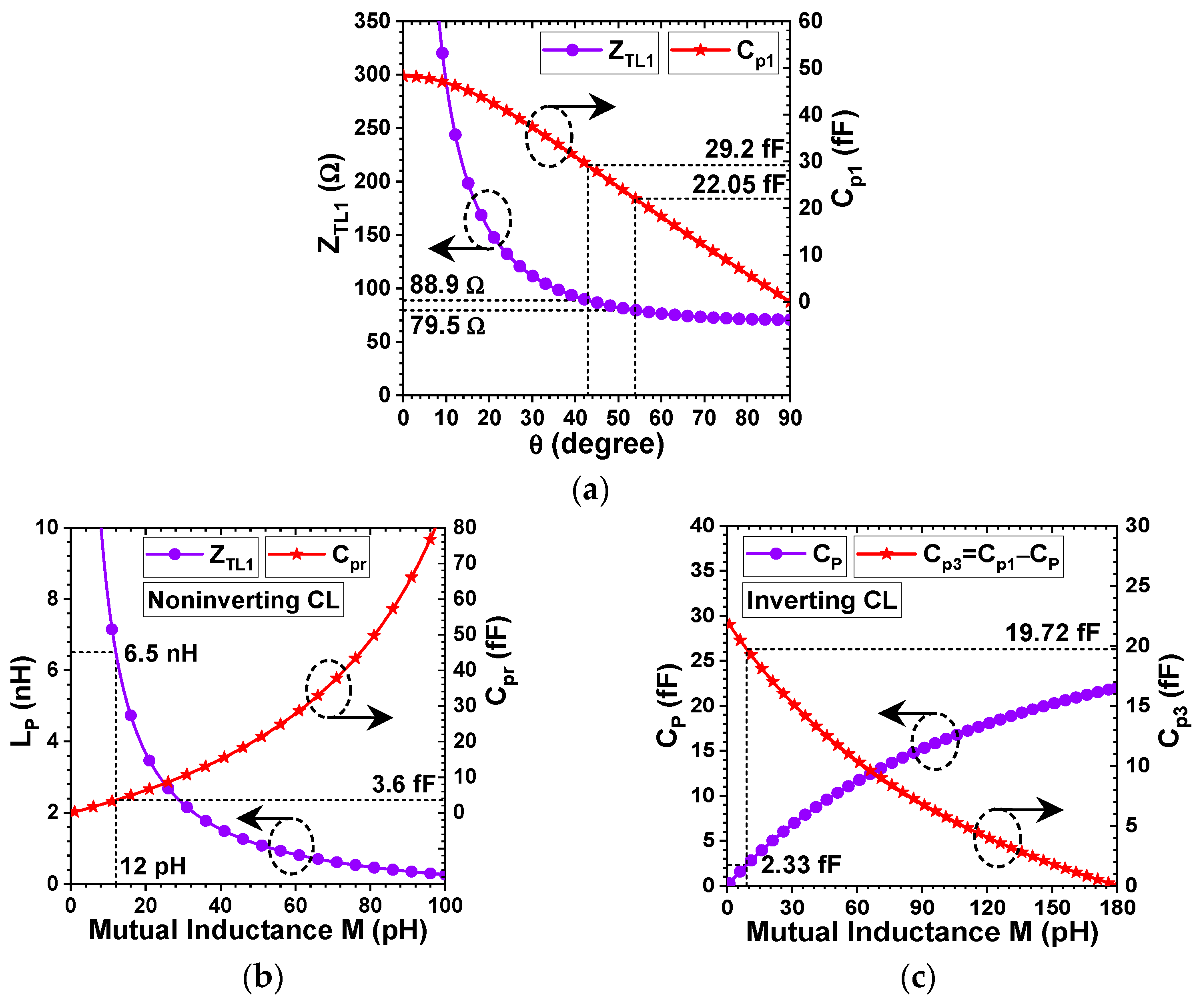
Figure 5a presents the simulation results of Z
TL1 and C
p1 of the lumped-distributed λ/4-TL-based two-way power splitter. Z
TL1 and C
p1 increase with the reduction in θ. At θ of 90° (i.e., length of λ/4), Z
TL1 and C
p1 are 70.7 Ω and 0, respectively. At θ of 54°, Z
TL1 and C
p1 are 79.5 Ω and 22.05 fF, respectively. At θ of 42.9°, Z
TL1 and C
p1 are 88.9 Ω and 29.2 fF, respectively.
Figure 5b presents the simulation results of L
P and C
pr of the noninverting helical-CL-based two-way power splitter. L
P increases with the decrease in M, while C
pr decreases with the decrease in M. For M of 12 pH, the corresponding L
P and C
pr are 6.5 nH and 3.6 fF, respectively. This is reasonable since L
P and C
pr should be equal to infinite and zero, respectively, for M equal to 0.
Figure 5c presents the simulation results of C
P and C
p3 of the inverting helical-CL-based two-way power splitter. C
P decreases with the decrease in M, while C
p3 increases with the decrease in M. For M of 9 pH, the corresponding C
P and C
pr are 2.33 fF and 19.72 fF, respectively. This is reasonable since C
P and C
p3 should be equal to zero and 22.05 fF, respectively, for M equal to 0.
4. Four-Way Power Splitter Design
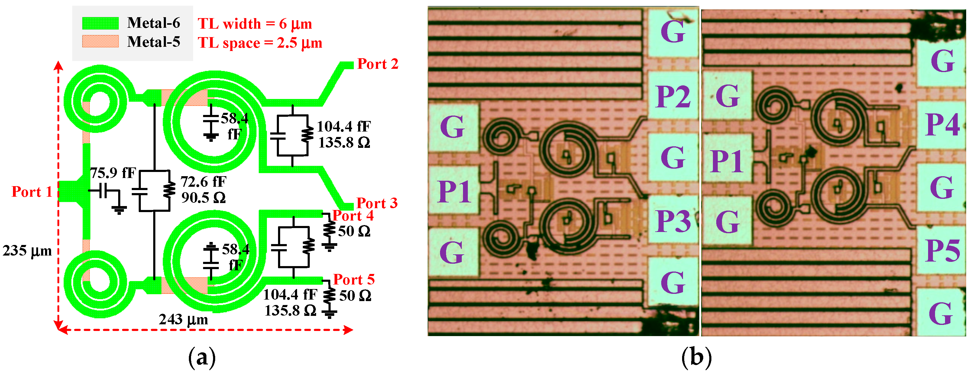
Figure 6a presents the simplified layout of PS1. PS1 consists of a double-helical two-way power splitter cascaded with two noninverting sole-helical two-way power splitters. Most of the TL structures are implemented using the top metal (i.e., the sixth metal layer), which has a thickness of 2.34 μm. The underlying interconnection lines are realized using the fifth metal layer with a thickness of 0.53 μm. The TL width and spacing are 6 μm and 2.5 μm, respectively. The chip size of the power splitter is 243 × 235 μm
2, i.e., 0.057 mm
2.
Figure 6b presents the chip microphotographs of PS1. The left image corresponds to the on-chip three-port measurement setup used to characterize the performance from port 1 to ports 2 and 3, and vice versa. The right image shows the setup for measuring performance from port 1 to ports 4 and 5, and vice versa.
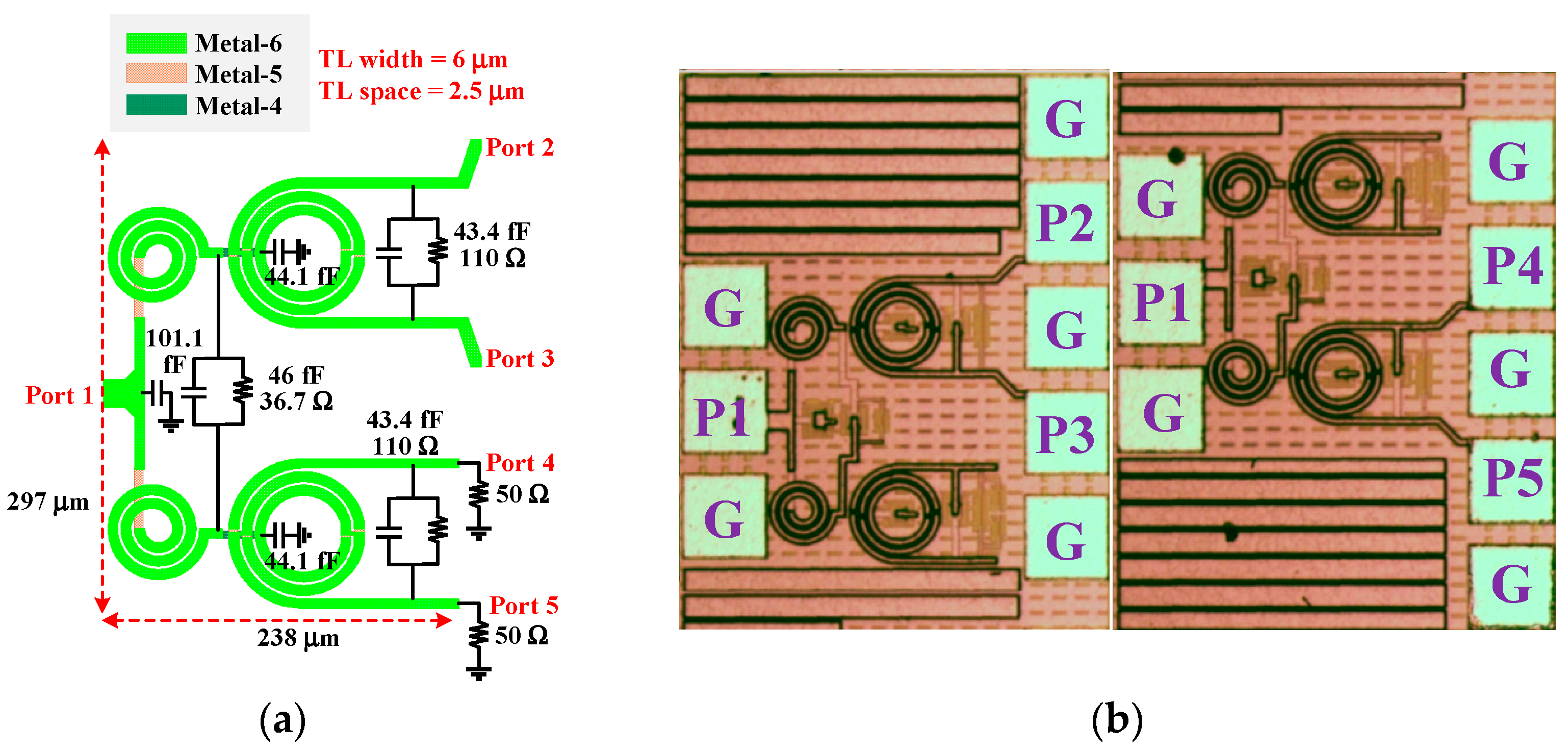
Figure 7a presents the simplified layout of PS2. PS2 consists of a double-helical two-way power splitter cascaded with two inverting sole-helical two-way power splitters. Most of the TL structures are implemented using the sixth metal layer. The underlying interconnection lines are realized by the fifth metal layer. The TL width and spacing are 6 μm and 2.5 μm, respectively. The chip size of the power splitter is 238 × 297 μm
2, i.e., 0.071 mm
2.
Figure 7b presents the chip microphotographs of PS2. The left image corresponds to the on-chip three-port measurement setup used to characterize the performance from port 1 to ports 2 and 3, and vice versa. The right image shows the setup for measuring performance from port 1 to ports 4 and 5, and vice versa.
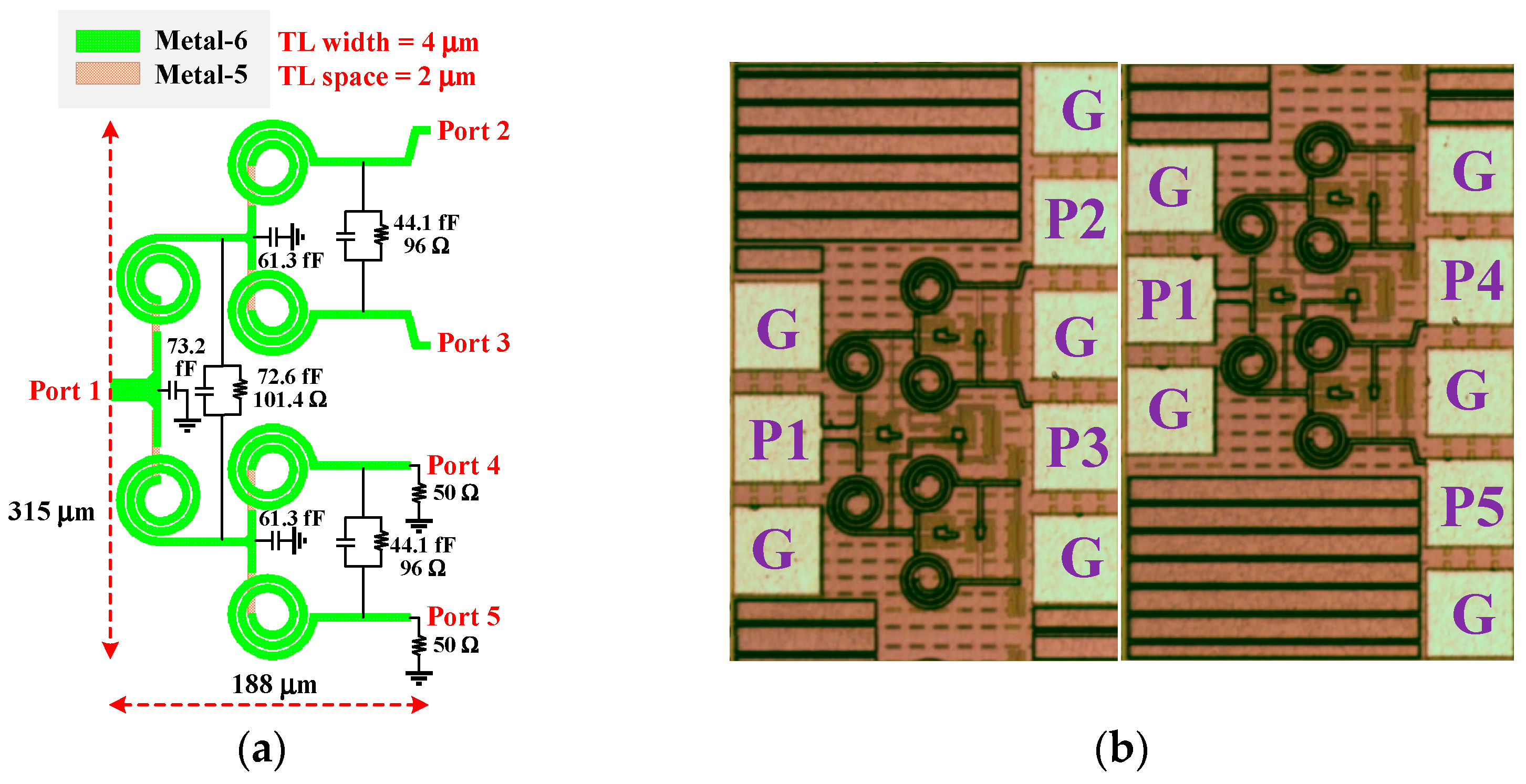
Figure 8a presents the simplified layout of PS3. PS3 consists of a double-helical two-way power splitter cascaded with two double-helical two-way power splitters. Most of the TL structures are implemented using the sixth metal layer. The underlying interconnection lines are realized by the fifth metal layer. The TL width and spacing are 4 μm and 2 μm, respectively. The chip size of PS3 is 188 × 315 μm
2, i.e., 0.059 mm
2, which is larger than that (0.057 mm
2) of PS1 due to the double-helical structure and smaller than that (0.071 mm
2) of PS2 due to smaller TL width and space being used.
Figure 8b presents the chip microphotograph of PS3. The left image corresponds to the on-chip three-port measurement setup used to characterize the performance from port 1 to ports 2 and 3, and vice versa. The right image shows the setup for measuring performance from port 1 to ports 4 and 5, and vice versa.
The rationale for proposing the three four-way power splitter designs—PS1, PS2, and PS3—is based on the trade-offs among chip size, transmission loss, impedance matching, and signal balance inherent in different two-way power splitter configurations. First, regarding the double-helical two-way power splitter, while this topology typically occupies a larger chip size, it provides superior input and output matching (S11 to S55) and robust overall performance, owing to the layout’s near symmetry. Second, regarding the non-inverting sole-helical two-way power splitter, this design generally offers a smaller chip size and improved overall performance, primarily due to lower TL loss. The reduced TL loss results from its shorter physical length due to the presence of positive mutual inductance between the helical TLs. Third, regarding the inverting sole-helical two-way power splitter, this configuration tends to occupy a medium chip size, as the negative mutual inductance between the TLs increases effective length. However, this configuration offers enhanced AI and PD performance because of its symmetrical geometry. Taking these trade-offs into consideration, the theoretically optimized four-way power splitter—achieving the smallest chip size and best overall performance—consists of a double-helical two-way power splitter cascaded with two non-inverting sole-helical two-way power splitters. This configuration is realized in PS1. For comparison, PS2 utilizes the same initial double-helical two-way power splitter but is cascaded with two inverting sole-helical two-way power splitters. Owing to its symmetrical structure, PS2 exhibits further improvements in AI and PD performance. PS3, representing a traditional topology, consists of a double-helical two-way power splitter cascaded with two additional double-helical two-way power splitters. It is included in this work to benchmark and contrast the performance of PS1.
5. Simulation Results of the Power Splitters
Figure 9a presents the simulation results of S
11, S
23, and S
45 of PS1. PS1 attains S
11 of −42.2 dB at 33 GHz, and S
11 better than −10 dB for 21.5–47.3 GHz. This corresponds to a −10 dB input matching bandwidth (f
10dB) of 25.8 GHz. In addition, PS1 attains S
23 of −40.4 dB at 33 GHz, and S
23 better than −10 dB for 26.8–39.7 GHz. This corresponds to a −10 dB isolation bandwidth (f
10dB,iso) of 12.9 GHz, which is comparable to that of S
45 (f
10dB,iso = 12.6 GHz, spanning from 26.8 GHz to 39.4 GHz).
Figure 9b presents the simulation results of S
22, S
33, S
44, and S
55 of PS1. PS1 attains S
22 of −30.2 dB at 33 GHz, and S
22 better than −10 dB for 12.9–56.5 GHz. This corresponds to an f
10dB of 43.6 GHz, which is comparable to that of S
33 (f
10dB = 42.6 GHz, spanning from 12.9 GHz to 56.5 GHz). In addition, PS2 attains S
44 of −30.5 dB at 33 GHz, and S
44 better than −10 dB for 12.9–55.9 GHz. This corresponds to an f
10dB,iso of 43 GHz, which is comparable to that of S
55 (f
10dB,iso = 43.3 GHz, spanning from 12.9 GHz to 56.2 GHz).
Figure 9c presents the simulation results of S
21, S
31, S
41, and S
51 of PS1. At 33 GHz, PS1 attains S
21 of −6.76 dB, which is close to the results for S
31 (−6.777 dB), S
41 (−6.779 dB), and S
51 (−6.77 dB). On the whole, the simulated S
21 closely matches S
31, S
41, and S
51, owing to the layout’s near symmetry.
Figure 9d presents the simulation results of AI
23, AI
24, AI
45, PD
23, PD
24, and PD
45 of PS1. At 33 GHz, PS1 attains a simulated AI
23 of 0.017 dB, which is close to AI
24 (0.004 dB) and AI
45 (−0.009 dB). This corresponds to an RMS error of AI is 0.011 dB at 33 GHz and ranges from 0.005 to 0.022 dB over the frequency range of 26–40 GHz. PS1 also attains a simulated PD
23 of 0.322° at 33 GHz, which is close to PD
24 (0.015°) and PD
45 (−0.293°). This corresponds to an RMS error of PD is 0.251° at 33 GHz and ranges from 0.175° to 0.294° over the 26–40 GHz frequency range.
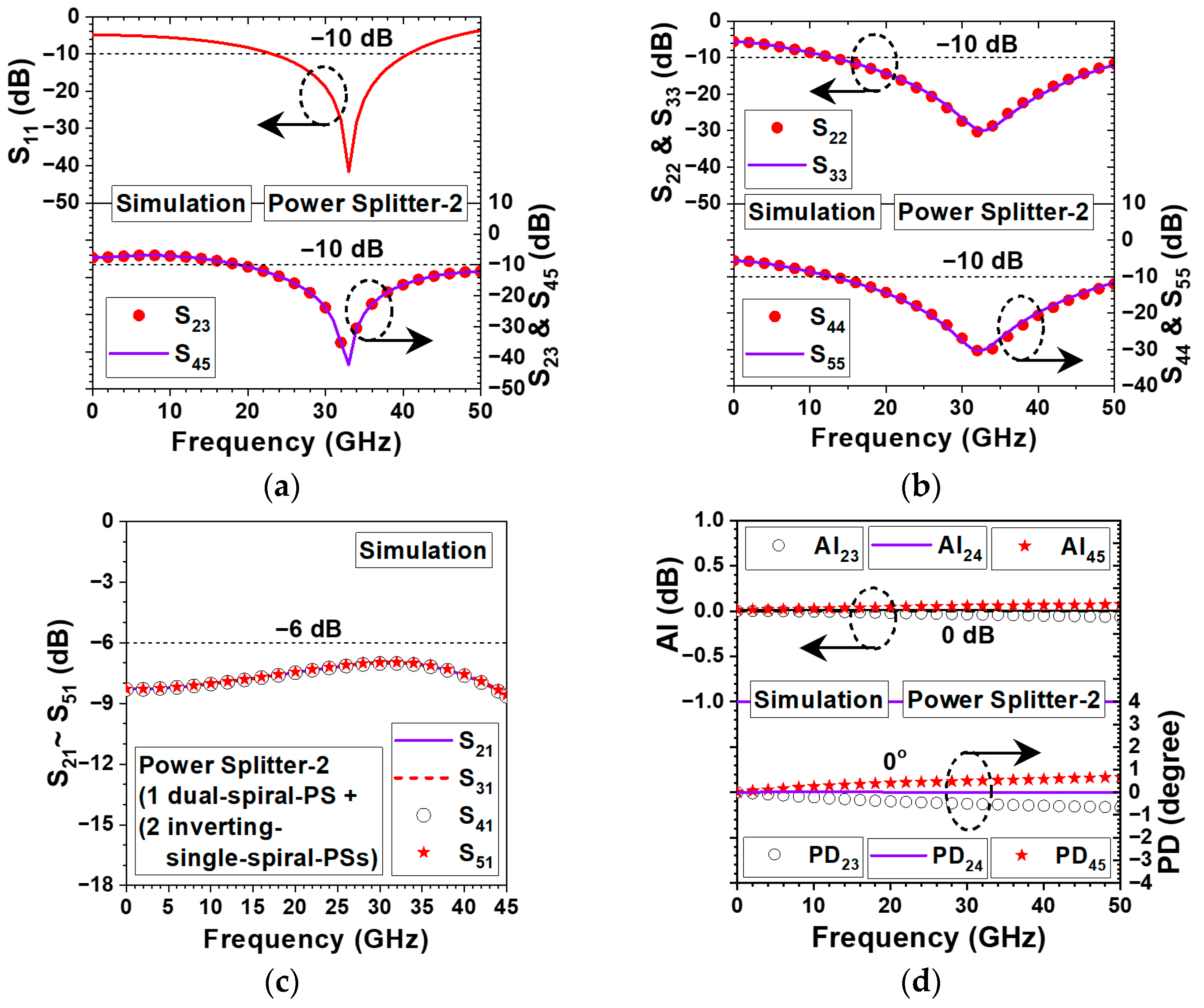
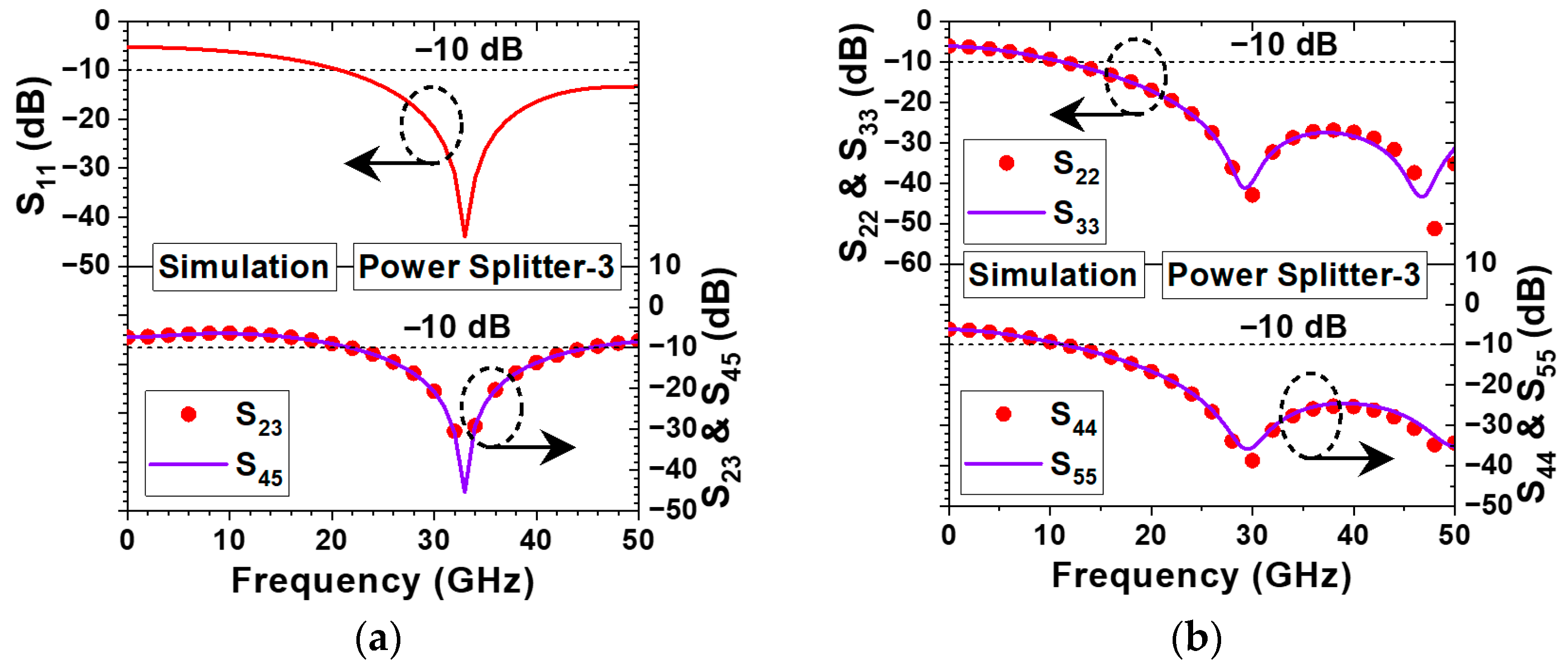
Figure 10a presents the simulation results of S
11, S
23, and S
45 of PS2. PS2 attains S
11 of −41.6 dB at 33 GHz, and S
11 better than −10 dB for 23.1–40.7 GHz. This corresponds to an f
10dB of 17.6 GHz. In addition, PS1 attains S
23 of −41.2 dB at 33 GHz, and S
23 better than −10 dB for 18.9–57.1 GHz. This corresponds to an f
10dB,iso of 38.2 GHz, comparable to that of S
45 (f
10dB,iso = 38.3 GHz, spanning from 18.9 GHz to 57.2 GHz).
Figure 10b presents the simulation results of S
22, S
33, S
44, and S
55 of PS2. PS2 attains S
22 of −30 dB at 33 GHz, and S
22 better than −10 dB for 12.9–52.6 GHz. This corresponds to an f
10dB of 39.7 GHz, comparable to that of S
33 (f
10dB = 39.9 GHz, spanning from 13.1 GHz to 53 GHz). In addition, PS2 attains S
44 of −30.7 dB at 33 GHz, and S
44 better than −10 dB for 13–53 GHz. This corresponds to an f
10dB,iso of 40 GHz, comparable to that of S
55 (f
10dB,iso = 39.7 GHz, spanning from 12.9 GHz to 52.6 GHz).
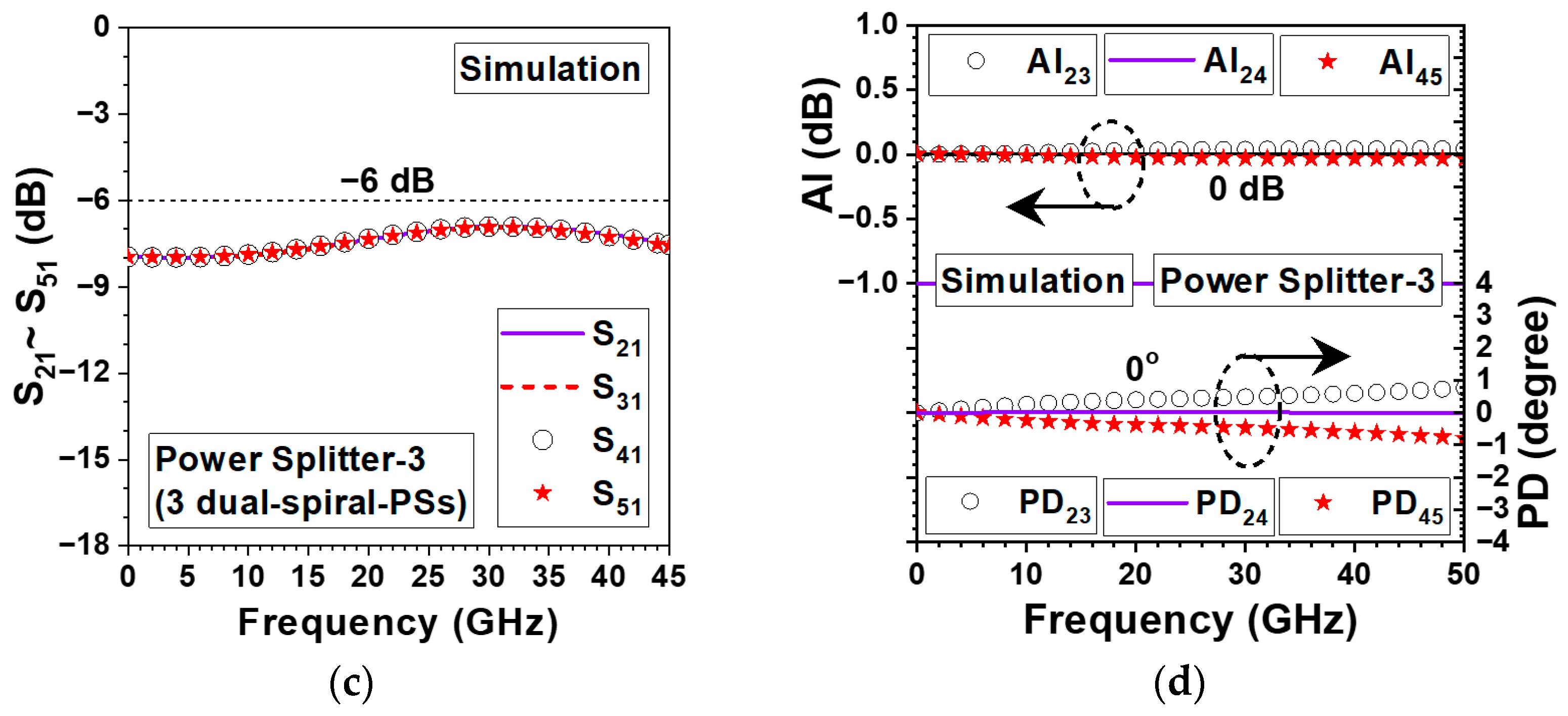
Figure 10c presents the simulation results of S
21, S
31, S
41, and S
51 of PS2. At 33 GHz, PS2 attains a simulated S
21 of −7.03 dB, which is closely matched by S
31 (−6.988 dB), S
41 (−6.984 dB), and S
51 (−7.041 dB). On the whole, the simulated S
21 closely matches S
31, S
41, and S
51, owing to the layout’s near symmetry.
Figure 10d presents the simulation results of AI
23, AI
24, AI
45, PD
23, PD
24, and PD
45 of PS2. At 33 GHz, PS2 attains a simulated AI
23 of −0.042 dB, which is closely matched by AI
24 (0.008 dB) and AI
45 (0.058 dB). This corresponds to an RMS error of AI is 0.042 dB at 33 GHz and ranges from 0.034 to 0.047 dB over the frequency range of 26–40 GHz. PS2 also attains a simulated PD
23 of −0.534° at 33 GHz, which is closely matched by PD
24 (−0.007°) and PD
45 (0.52°). This corresponds to an RMS error of PD of 0.43° at 33 GHz and ranging from 0.38° to 0.478° over the 26–40 GHz frequency range.
Figure 11a presents the simulation results of S
11, S
23, and S
45 of PS3. PS3 attains S
11 of −43.9 dB at 33 GHz, and S
11 better than −10 dB for 20.8–60.3 GHz. This corresponds to an f
10dB of 39.5 GHz. In addition, PS1 attains S
23 of −43.2 dB at 33 GHz, and S
23 better than −10 dB for 21.9–45 GHz. This corresponds to an f
10dB,iso of 23.1 GHz, comparable to that of S
45 (f
10dB,iso = 23.4 GHz, spanning from 21.8 GHz to 45.2 GHz).
Figure 11b presents the simulation results of S
22, S
33, S
44, and S
55 of PS3. PS3 attains S
22 of −30.2 dB at 33 GHz, and S
22 better than −10 dB from 11.2 GHz to larger than 50 GHz. This corresponds to an f
10dB larger than 38.8 GHz, comparable to that of S
33 (f
10dB larger than 38.8 GHz, from 11.2 to larger than 50 GHz). In addition, PS3 attains S
44 of −29 dB at 33 GHz, and S
44 better than −10 dB from 11.3 GHz to larger than 50 GHz. This corresponds to an f
10dB,iso larger than 38.7 GHz, comparable to that of S
55 (f
10dB,iso larger than 38.7 GHz, from 11.3 GHz to larger than 50 GHz).
Figure 11c presents the simulation results of S
21, S
31, S
41, and S
51 of PS3. At 33 GHz, PS3 attains a simulated S
21 of −6.914 dB, which is comparable to S
31 (−6.953 dB), S
41 (−6.966 dB), and S
51 (−6.934 dB). On the whole, the simulation results of S
21, S
31, S
41, and S
51 are closely matched, attributed to the layout’s near symmetry.
Figure 11d presents the simulation results of AI
23, AI
24, AI
45, PD
23, PD
24, and PD
45 of PS3. At 33 GHz, PS3 attains a simulated AI
23 of 0.04 dB, which is comparable to AI
24 (0.004 dB) and AI
45 (−0.032 dB). At 33 GHz, the RMS error of AI is 0.03 dB. Over 26–40 GHz, it ranges from 0.027 to 0.030 dB. PS3 also attains a simulated PD
23 of 0.519° at 33 GHz, which is comparable to PD
24 (0.006°) and PD
45 (−0.508°). This corresponds to an RMS error of PD of 0.419° at 33 GHz and ranging from 0.36° to 0.493° over the 26–40 GHz frequency range.
Table 1 presents the simulated RMS errors for AI and PD at temperatures of −25 °C, 25 °C, and 75 °C for the four-way power splitters PS1–PS3, operating at 33 GHz. At 25 °C, PS1 records RMS errors of 0.011 dB for AI and 0.251° for PD, which are comparable to the values observed at −25 °C (0.008 dB and 0.212°) and 75 °C (0.015 dB and 0.341°). Likewise, PS2 yields RMS errors of 0.042 dB for AI and 0.43° for PD at 25 °C, closely aligning with those at −25 °C (0.029 dB and 0.311°) and 75 °C (0.059 dB and 0.581°). For PS3, the RMS errors at 25 °C are 0.03 dB for AI and 0.419° for PD, which are similar to the results at −25 °C (0.021 dB and 0.308°) and 75 °C (0.039 dB and 0.579°). These consistent error values across the temperature range are expected, as PS1–PS3 are all helical-line-based passive components. As noted in [
12,
13,
14], the model parameters of CMOS helical-line inductors and transformers (i.e., coupled inductors) exhibit minimal sensitivity to temperature variations.
6. Measurement Results and Discussion
On-wafer three-port scattering-parameter (S-parameter) measurements for PS1–PS3 were conducted over the 0.1–50 GHz frequency range using an Agilent N5247A PNA-X microwave network analyzer. Calibration was performed up to the probe tips using a short–load–open–through (SLOT) method with an RF calibration substrate. This approach enables accurate de-embedding of cable losses—measured to be 4 dB at 28 GHz and 4.8 dB at 39 GHz—and corrects for systematic errors in the measurement setup.
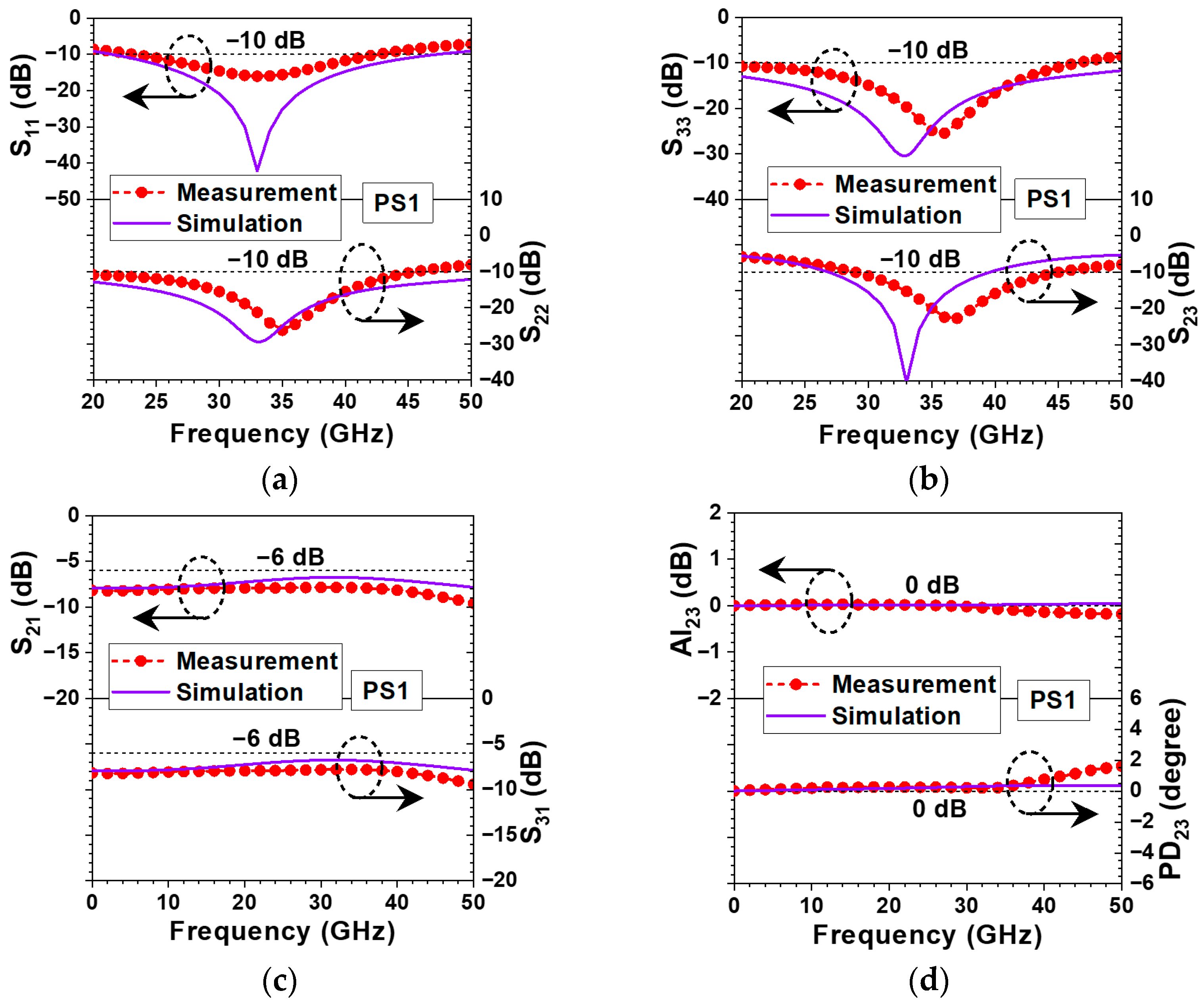
Figure 12a compares the measured and simulated S
11 and S
22 responses for PS1. The measured S
11 reaches −16 dB at 33 GHz and stays below −10 dB across 23.2–42.6 GHz (f
10dB = 19.4 GHz). This is in line with simulation results showing S
11 of −42.2 dB at 33 GHz and below −10 dB across 21.5–47.3 GHz (f
10dB = 25.8 GHz). For S
22, measurements indicate a value of −21.2 dB at 33 GHz, with performance remaining below −10 dB from 13.6 to 45.6 GHz (f
10dB = 32 GHz). Simulations yield similar results, showing −30.2 dB at 33 GHz and a −10 dB bandwidth extending from 13.1 to 56.5 GHz (f
10dB = 43.4 GHz).
Figure 12b illustrates the measured and simulated S
33 and S
23 of PS1. The measured S
33 is −19.7 dB at 33 GHz and remains below −10 dB over the 13.9–46.6 range. This corresponds to an f
10dB of 32.7 GHz, closely aligning with the simulated S
33, which reaches −31.3 dB at 33 GHz and remains at −10 dB from 12.8 to 55.8 GHz (f
10dB = 43 GHz). For S
23, the measured value at 33 GHz is −15.3 dB, and the −10 dB isolation bandwidth spans from 28.8 to 45.2 GHz (f
10dB,iso = 16.4 GHz). This result aligns well with the simulated S
23, which shows −40.4 dB at 33 GHz and −10 dB bandwidth from 26.8–39.7 GHz (f
10dB,iso = 12.9 GHz).
Figure 12c displays the measurement and simulation results of S
21 and S
31 of PS1. At 33 GHz, the measured S
21 and S
31 are −7.862 dB and −7.803 dB, respectively, which are closely aligned with the simulated values of −6.76 dB (S
21) and −6.777 dB (S
31). Across the 26–40 GHz frequency range, the measured S
21 and S
31 closely align with the simulations.
Figure 12d presents the measurement and simulation results of AI
23 and PD
23 of PS1. At 33 GHz, the measured AI
23 is −0.059 dB and PD
23 is 0.197°, both of which are closely aligned with the simulated values of 0.017 dB (AI
23) and 0.322° (PD
23). The respective measured RMS errors—0.056 dB for AI and 0.181° for PD—closely align with the simulated counterparts of 0.011 dB and 0.251°, respectively. On the whole, the measured AI and PD characteristics of PS1 show strong alignment with the simulation results.
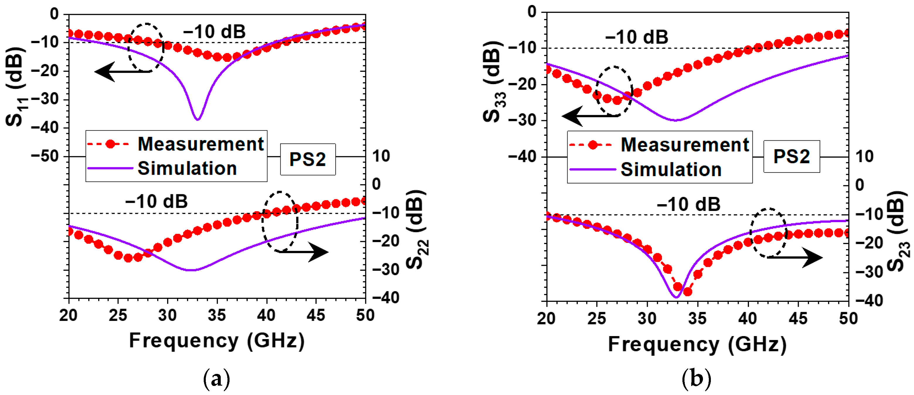
Figure 13a presents the measurement and simulation results of S
11 and S
22 of PS2. At 33 GHz, PS2 exhibits a measured S
11 of −13.5 dB and remains S
11 below −10 dB across the 28.6–41.6 GHz range (f
10dB = 13 GHz). This aligns well with the simulated S
11, which reaches −41.6 dB at 33 GHz and remains below −10 dB from 23.2 to 40.7 GHz (f
10dB = 17.5 GHz)). The measured S
22 is −16.1 dB at 33 GHz, with a −10 dB bandwidth spanning 11.8–40.3 GHz (f
10dB = 28.5 GHz), closely matching the simulation result of −30 dB at 33 GHz and −10 dB bandwidth from 12.9 to 52.6 GHz (f
10dB = 39.7 GHz).
Figure 13b presents the measurement and simulation results of S
33 and S
23 of PS2. The measured S
33 is −16.7 dB at 33 GHz and remains below −10 dB from 11.9 to 40.7 GHz (f
10dB = 28.8 GHz), in line with the simulated S
33 of −30.1 dB at 33 GHz and −10 dB bandwidth of 13.1–53 GHz (f
10dB = 39.9 GHz). For S
23, the measured values at 33 GHz are −34.8 dB, with a −10 dB bandwidth extending from 19.2 to 62.3 GHz (f
10dB = 43.1 GHz), closely matching the simulated S
23 of −41.2 dB at 33 GHz and bandwidth of 18.9–57 GHz (f
10dB,iso = 38.1 GHz).
Figure 13c displays the measurement and simulation results of S
21 and S
31 of PS2. At 33 GHz, the measured S
21 and S
31 are −8.1 dB and −8.146 dB, respectively, which are closely aligned with the simulated values of −7.03 dB (S
21) and −6.988 dB (S
31). Across the 26–40 GHz frequency range, the measured S
21 and S
31 are in line with the simulated results.
Figure 13d presents the measurement and simulation results of AI
23 and PD
23 of PS2. At 33 GHz, the measured AI
23 is 0.046 dB and PD
23 is −0.581°, both of which are closely aligned with the simulated values of −0.042 dB (AI
23) and −0.534° (PD
23). The respective measured RMS errors—0.045 dB for AI and 0.572° for PD—closely align with the simulated counterparts of 0.042 dB and 0.43°, respectively. On the whole, the measured AI and PD characteristics of PS2 show strong alignment with the simulation results.
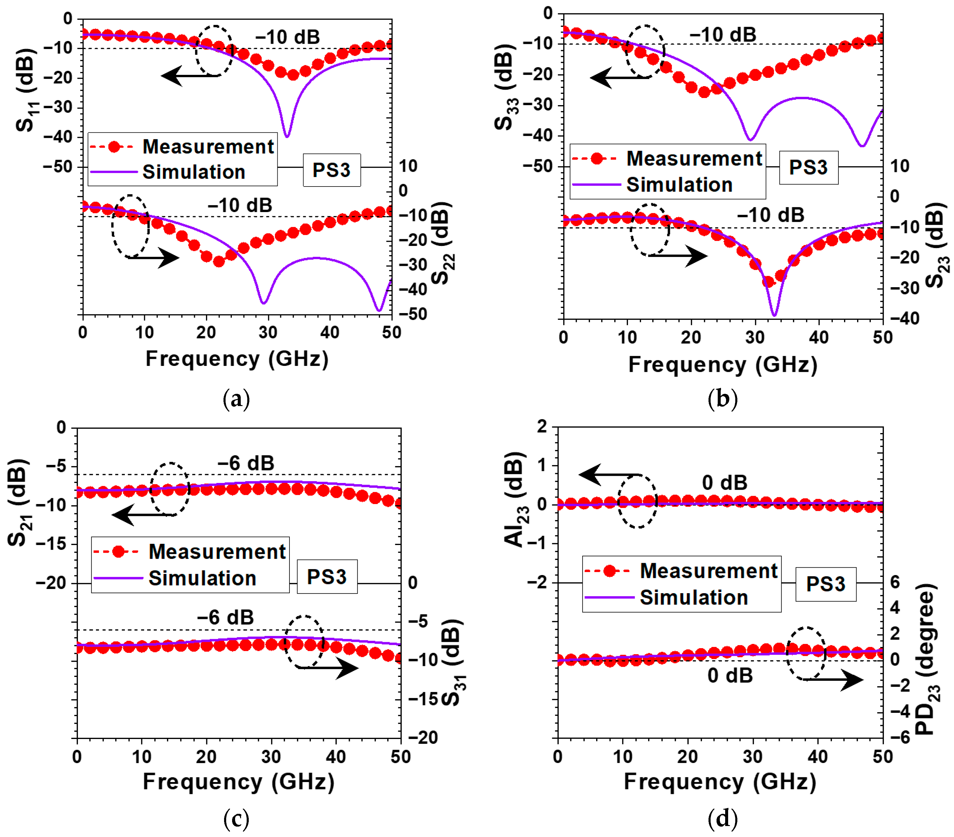
Figure 14a presents the measurement and simulation results of S
11 and S
22 of PS3. At 33 GHz, PS3 exhibits a measured S
11 of −18.7 dB and remains S
11 below −10 dB across the 23.3–45 GHz range (f
10dB = 21.7 GHz). This aligns well with the simulated S
11, which reaches −43.9 dB at 33 GHz and remains below −10 dB from 20.7 to 60.2 GHz (f
10dB = 39.5 GHz). The measured S
22 is −17.3 dB at 33 GHz, with a −10 dB bandwidth spanning 8.8–44 GHz (f
10dB = 35.2 GHz), closely matching the simulation result of −30.2 dB at 33 GHz and −10 dB bandwidth from 11.2 to 54.5 GHz (f
10dB = 43.3 GHz).
Figure 14b presents the measurement and simulation results of S
33 and S
23 of PS3. The measured S
33 is −18.5 dB at 33 GHz and remains below −10 dB from 8.9 to 45.3 GHz (f
10dB = 36.4 GHz), in line with the simulated S
33 of −30.2 dB at 33 GHz and −10 dB bandwidth of 13.1–53 GHz (f
10dB = 43.7 GHz). For S
23, the measured values at 33 GHz is −28.2 dB, with a −10 dB bandwidth extending from 20.9 to 57.1 GHz (f
10dB = 36.2 GHz), closely matching the simulated S
23 of −43.2 dB at 33 GHz and bandwidth of 21.9–44.9 GHz (f
10dB,iso = 23 GHz).
Figure 14c displays the measurement and simulation results of S
21 and S
31 of PS3. At 33 GHz, the measured S
21 and S
31 are −7.828 dB and −7.879 dB, respectively, which closely align with the simulated values of −6.914 dB (S
21) and −6.953 dB (S
31). Across the 26–40 GHz frequency range, the measured S
21 and S
31 are in line with the simulated results.
Figure 14d presents the measurement and simulation results of AI
23 and PD
23 of PS3. At 33 GHz, the measured AI
23 is 0.051 dB and PD
23 is 0.894°, both of which are closely aligned with the simulated values of 0.04 dB (AI
23) and 0.519° (PD
23). The respective measured RMS errors—0.049 dB for AI and 0.782° for PD—closely align with the simulated counterparts of 0.03 dB and 0.419°, respectively. On the whole, the measured AI and PD characteristics of PS3 show strong alignment with the simulation results.
Table 2 presents a comparison of the performance metrics of PS1–PS3 against recently published state-of-the-art four-way power splitters operating within comparable frequency ranges. Among them, PS1 stands out as one of the most efficient designs documented in the literature, offering exceptional performance in terms of compact chip size, input/output return loss (S
11 and S
22), wide input matching bandwidth, low transmission loss, minimal amplitude inequality, and reduced phase deviation. These characteristics position PS1 as a leading contender among K/Ka-band four-way power splitters. Likewise, PS2 delivers superior results in S
11/S
22, input-matching bandwidth, inter-port isolation and its corresponding bandwidth, and amplitude balance—ranking it among the top-performing designs reported to date. PS3 also performs impressively across these parameters, particularly excelling in input matching and isolation bandwidths.
The ideal role of the four-way power splitters discussed in this article is to evenly divide an input signal into four output signals—each with equal amplitude (carrying one-quarter of the input power) and identical phase—across the 26.5–40 GHz frequency band, and vice versa. To account for practical non-idealities such as resistive losses and layout-induced asymmetries, the designs were optimized to meet the following targets: reflection coefficients (S11 to S55) below −10 dB, transmission coefficients (S21 to S51) above −8.2 dB, output-to-output isolation better than −15 dB, AIM less than 0.1 dB, and PDM under 1°. All three designs—PS1, PS2, and PS3—not only satisfy these performance criteria but also feature ultra-compact footprints (<0.01 mm2), making them well-suited for integration into 28–32 GHz Ka-band LEO SATCOM transmitters and 26.5–29.5/37–40 GHz Ka-band 5G radio systems.
Furthermore, a comparison of the three designs yields the following insights: First, PS1 utilizes a double-helical two-way power splitter followed by two non-inverting sole-helical two-way power splitters. This configuration delivers the smallest chip size and the best overall performance, making it a highly effective topology for compact, high-performance applications. Second, PS2 features a double-helical two-way power splitter cascaded with two inverting sole-helical two-way splitters. Its symmetric layout leads to the lowest AIM and the broadest output-to-output isolation bandwidth, positioning PS2 as the preferred choice for systems requiring precise signal balance and strong isolation. Finally, PS3 is composed of a double-helical two-way splitter cascaded with two additional double-helical two-way splitters. This architecture provides the widest frequency bandwidth for input/output return loss (S11 and S22), making PS3 especially well-suited for broadband applications that demand wide input matching.
