1. Introduction
The demand for low-power, efficient computational architectures has grown in response to the increasing use of artificial intelligence (AI) and machine learning applications.The limitations of the traditional von Neumann design, which has significant data transmission inefficiencies, can be addressed by computing in-memory (CIM). Because CIM integrates processing directly into memory, it reduces power consumption and data transmission delay, making it perfect for applications requiring high performance and low energy usage [
1].
One significant area where CIM is beneficial is in the execution of binary and ternary computations. Binary Neural Networks (BNNs) use binarized activations and weights (+1, −1) to convert Multiply-And-Accumulate (MAC) operations into XNOR operations, which has demonstrated significant improvements in computing performance.
Matrix multiplication, a fundamental task in AI workloads, is made simpler as a result [
2]. Even more potential for nuanced computations is provided by Ternary Neural Networks (TNNs), which expand on this idea by permitting inputs to have values of +1, 0, and −1. Compared to BNNs, TNNs maintain low power requirements while improving accuracy by striking a balance between computational economy and representational flexibility [
3].
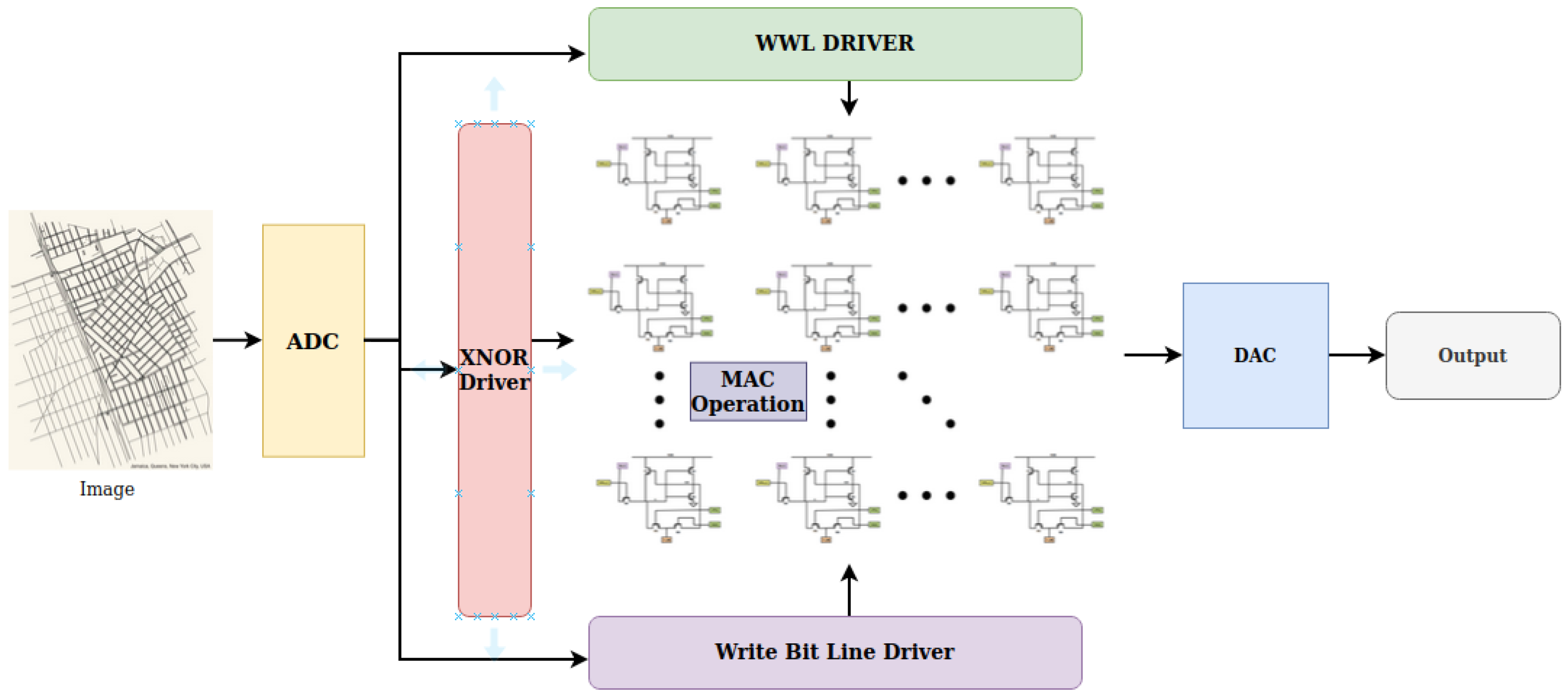
A possible use case of Compute-In-Memory (CIM) architecture in image processing is shown in
Figure 1. Using an Analog-to-Digital Converter (ADC), the system first transforms an input image into digital signals. An XNOR driver receives these signals and obtains the data ready for in-memory calculation. Utilizing the effectiveness of in-memory logic, the memory array, comprising several bit-cells, executes Multiply–Accumulate (MAC) operations in parallel. Read/write access to the memory cells is controlled by the word line (WWL) and bit line drivers. Lastly, a Digital-to-Analog Converter (DAC) transforms the calculated findings back into analog form before sending them to the output stage. This architecture minimizes data travel between memory and logic units, highlighting low-power, high-speed data processing.
According to the study’s findings, the proposed 6T SRAM design has the potential to significantly advance the development of ultra-low-power CIM architectures, which are essential for next-generation AI accelerators and embedded systems [
4]. In the rapidly evolving landscape of AI-driven technologies, emphasizing ternary computations can further enhance speed and energy efficiency, paving the way for more scalable and effective CIM solutions. Moreover, integrating CIM with Processing-In-Memory (PIM) systems offers substantial improvements in computational efficiency by minimizing data movement and facilitating faster processing directly within memory [
5,
6]. This synergy between CIM and PIM architectures could fundamentally reshape memory-centric AI accelerators, providing a more effective approach for managing increasingly complex workloads.
2. Background
Large amounts of data often necessitate parallel processing in AI-related applications, which in turn increases energy consumption. SRAM-based computing-in-memory (CIM) addresses these challenges by enabling operations directly within the memory array, thereby reducing both power consumption and data transfer. Ternary logic further enhances energy efficiency by minimizing the number of logic operations, leading to designs that consume less power than conventional binary systems [
7,
8]. In ternary logic systems, the XNOR gate plays a vital role, particularly in arithmetic and comparison operations. The use of 8T SRAM cells with ternary XNOR gates enables efficient in-memory processing, enhancing speed while reducing both power consumption and delay. These features make them ideal for AI applications that demand rapid data processing and low power consumption.
2.1. A 6T SRAM Cell
The proposed 6T SRAM design delivers substantial improvements in power and delay performance compared to traditional 10T SRAM cells. Key advantages include a simplified architecture, which reduces switching activity and results in lower power consumption. While the 10T SRAM achieves better read stability by fully separating read and write channels, it does so with the addition of extra transistors, which increases switching and power consumption. In contrast, the 6T SRAM’s fewer signal transitions result in shorter access times. Its reduced transistor count makes it particularly suitable for low-power applications by minimizing both dynamic and leakage power, which is critical for energy-constrained environments such as edge devices and real-time CIM processing.
2.2. Pass Transistor Logic
Pass transistor logic (PTL) is a digital circuit design technique in which transistors transmit signals directly, rather than toggling between voltage levels. Traditional CMOS logic uses both PMOS and NMOS transistors to drive either high or low outputs [
9], while PTL employs transistors as switches to selectively permit or block voltage signals. PTL can lead to lower power consumption, reduced transistor count, and faster switching speeds. NMOS transistors in PTL pass a strong “0,” while PMOS handles a strong “1.” Combining both achieves full-swing signal [
10].
3. XNOR Operation in Ternary Logic Using Pass Transistor Logic (PTL)
In traditional binary logic, the XNOR gate outputs “1” when its inputs are equal and “0” when they differ. In ternary logic systems, however, the high and low states correspond to +1 and −1, while the XNOR gate outputs a neutral state (0) when the inputs are balanced [
11]. As shown in
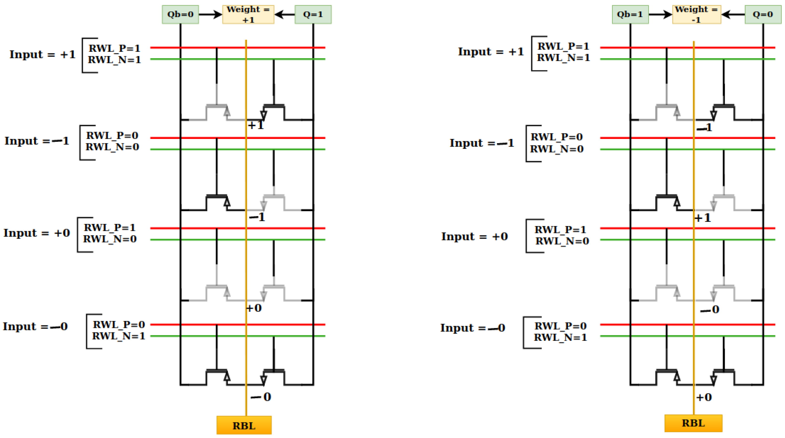
Figure 2 the PTL-based ternary XNOR gate operates within a cell storing Q and Qb. Two control signals, RWL_P and RWL_N, determine the output logic, corresponding to the weight–input relationship mapped in
Table 1. In ternary logic systems, the XNOR gate’s ability to efficiently handle arithmetic and comparison functions is essential. Enabling in-memory processing with 6T SRAM cells and ternary XNOR gates enhances speed while minimizing power and latency, making these cells well-suited for AI applications that require fast data handling and low energy consumption. The pass transistor logic of our design is depicted in
Figure 2. The
weight value is
−1 when Q = 0 and Qb = 1, and
+1 when Q = 1 and Qb = 0.
Figure 2 demonstrates pass transistor operations for these weights and a variety of input values, with corresponding outputs also shown. In
Figure 2,
RWL_P and
RWL_N serve as inputs to the PMOS and NMOS transistors, respectively. Below, we explain the pass transistor logic operation for a weight value of +1 (Q = 1, Qb = 0):
XNOR Output (+1): When RWL_P = 1 and RWL_N = 1, the input value is +1. For this particular input combination, the NMOS will be turned on, and the output will be high, +1.
XNOR Output (−1): When RWL_P = 0 and RWL_N = 0, the input value is −1. For this particular input combination, PMOS will be turned on and the multiplication result will be −1.
XNOR Output (+0): When RWL_P = 1 and RWL_N = 0, the input value is +0. In this case, both the PMOS and NMOS transistors are turned off, resulting in no current flow. Hence, the output voltage remains at +0 (no change).
XNOR Output (−0): In this scenario, both the PMOS and NMOS transistors are on, as RWL_P and RWL_N are 1 and 0, respectively. However, due to the stronger pull-down effect of the NMOS transistor, the output node is pulled down to a low voltage level. Therefore, the output of the pass transistor logic will be −0.
4. Proposed CIM Design
In this paper, we propose a pass transistor-based CIM architecture utilizing both NMOS and PMOS transistors. Signal RWL_N is applied to the NMOS transistor, while signal RWL_P is applied to the PMOS transistor. The combination of these inputs determines the actual input value, and the states of Q and Qb represent the weight value, as summarized in
Table 1. Key advantages of the proposed architecture are its flexible integration with various SRAM structures, as well as substantial reductions in power and delay compared to conventional 10T SRAM designs. We present three designs based on PLNA (P-Latch N-Access), NLPA (N-Latch P-Access), and SE (Single-Ended) SRAM structures, all integrated with XNOR-based pass transistor logic. Our designs are compared against a conventional 10T SRAM cell, demonstrating equivalent performance while achieving these benefits.
4.1. P-Latch N-Access (PLNA) SRAM Structure
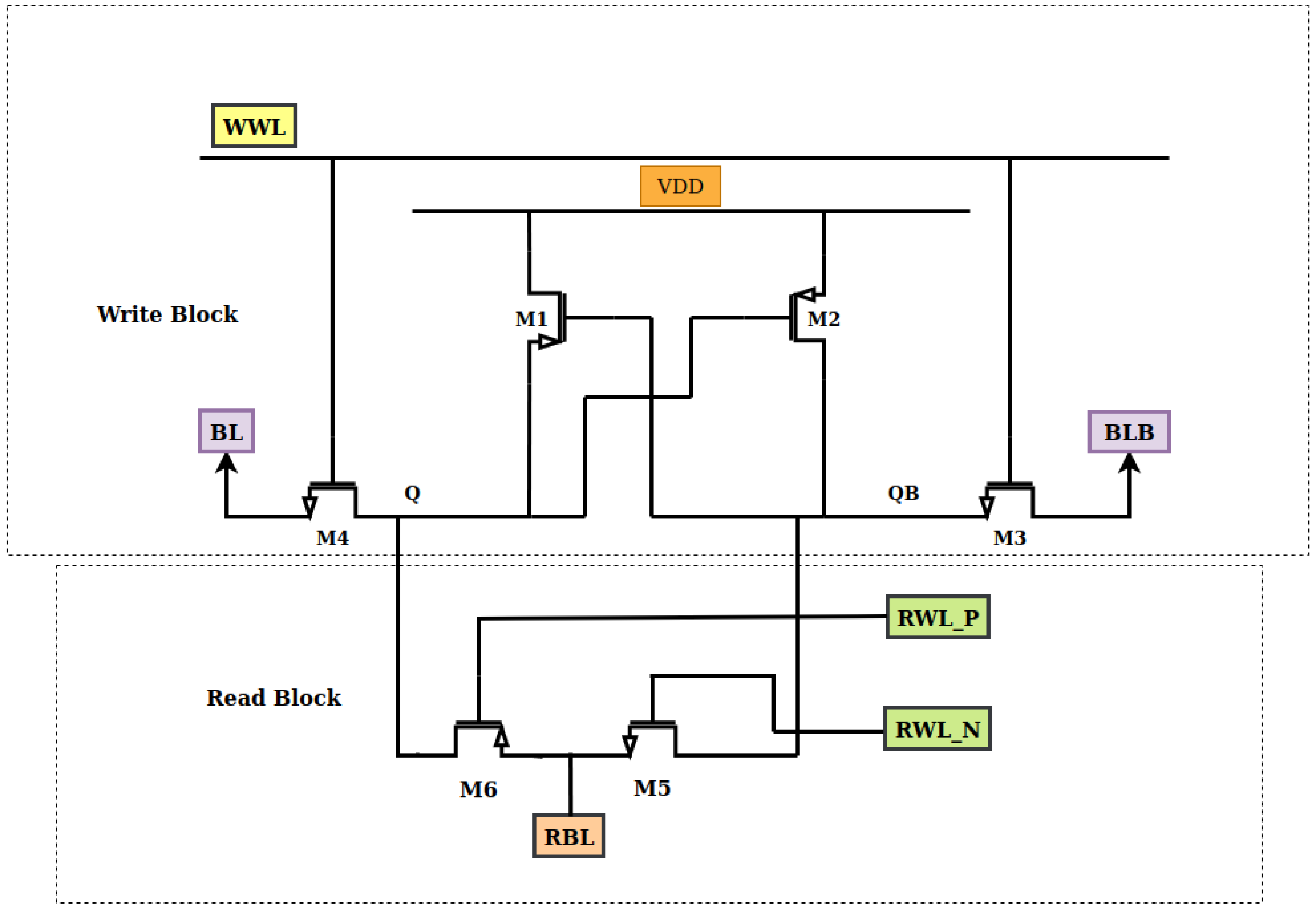
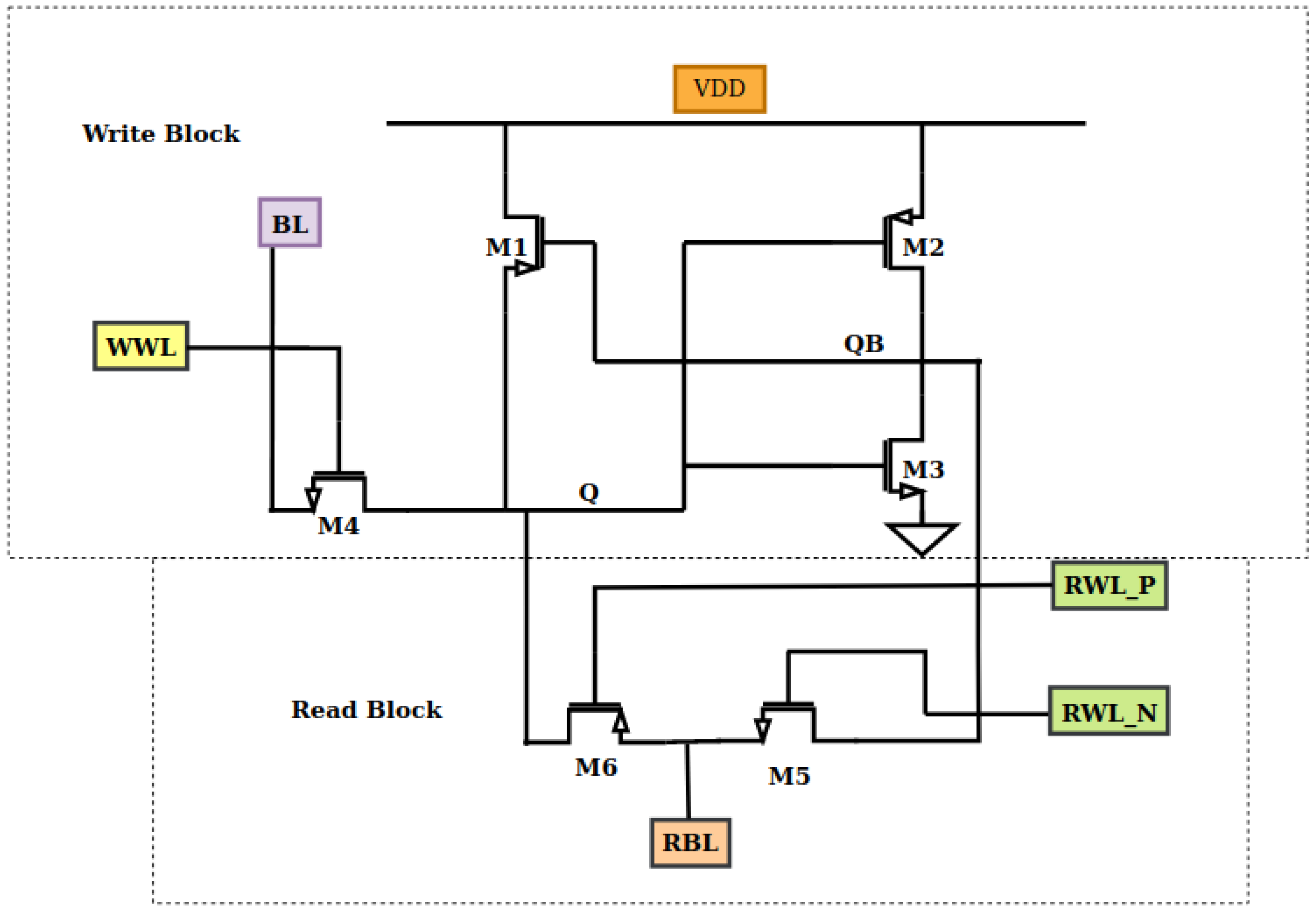
The proposed PLNA 6T SRAM cell distinguishes itself from conventional SRAM by separating the read and write circuitry, as illustrated in
Figure 3. The primary motivation behind this separation is to reduce power consumption and delay. Traditional SRAM cells often combine read and write operations in a single circuit, which can lead to unnecessary switching activity and increased power consumption [
12]. In contrast, the PLNA 6T cell separates the read and write paths, allowing these functions to operate independently. This isolation eliminates unnecessary switching in the read circuitry during write operations, leading to substantial power savings. Additionally, this approach reduces the likelihood of rapid current flow between the latch and access transistors—a common issue in traditional SRAM designs. By employing only two transistors (M1 and M2) in the latch, the PLNA minimizes the number of active elements required to hold data compared to conventional SRAM designs [
13]. This configuration significantly reduces current flow during write operations, enabling faster and more efficient writes without compromising performance. The decoupled architecture not only lowers power usage but also enhances write speed, making it highly advantageous in energy-sensitive applications. The main objective of the proposed 6T SRAM cell is to facilitate CIM operations, allowing essential logic to execute directly within memory. Our design focuses on performing neural network multiplications between inputs and weights using XNOR logic. The main advantages include minimized power consumption and delay through the achievement of CIM multiplication with just two transistors (one NMOS and one PMOS, as shown in
Figure 3), compared to the previous design’s four transistors. This reduction directly translates into lower power consumption and delay relative to the original design.
The
Table 2 below displays the transistor size for FinFET in PLNA in the suggested 6T SRAM cell. In the table below, the
number of FINS represents the number of parallel
FIN structures using which the transistor was created. The size of M5 (four FINs) and M6 (eight FINs) was intentionally skewed to ensure balanced pull-down and pull-up strength during linear accumulation, compensating for the weaker PMOS drive and enabling reliable analog summation at the shared output node.
4.2. N-Latch P-Access (NLPA) SRAM Structure
The NLPA architecture employs NMOS transistors in the cross-coupled latch and PMOS transistors for access control. NMOS devices are chosen for the latch due to their higher drive strength compared to PMOS, which enhances read stability [
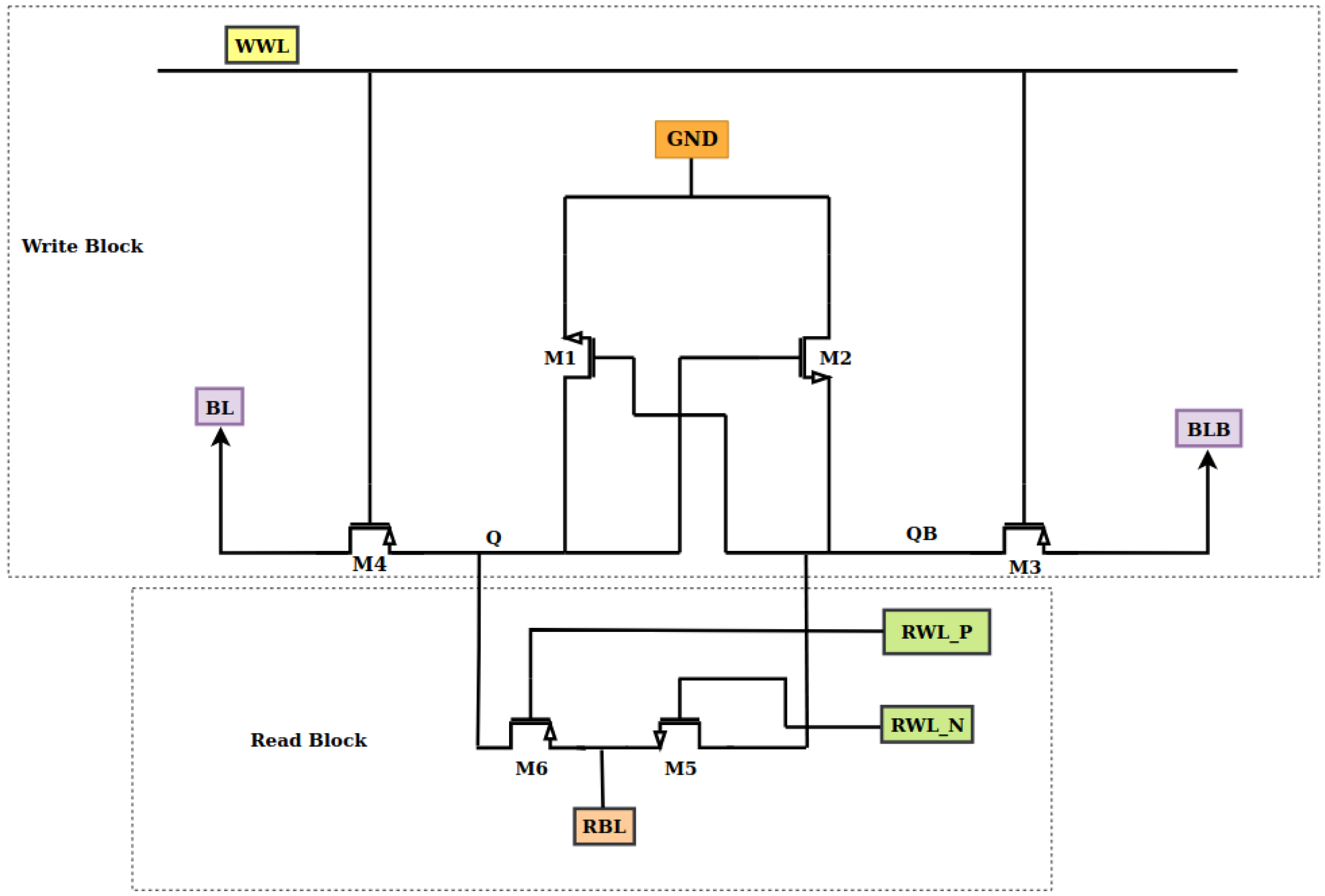
14]. The access path utilizes PMOS transistors, making the cell more power-efficient during standby, as PMOS devices exhibit low leakage when idle. In contrast, the P-Latch N-Access (PLNA) design, illustrated in
Figure 4, utilizes PMOS in the latch and NMOS as access transistors. This approach enhances the write margin, as NMOS access transistors offer robust pull-down and pull-up effects on internal nodes, particularly at lower supply voltages [
15]. However, the inherently slower switching speed of PMOS transistors may increase the delay in the PLNA design. Compared to PLNA, the NLPA architecture offers superior read reliability, which is critical for CIM operations where data stability is paramount. The proposed 6T SRAM cell is optimized for CIM applications, allowing basic logic—specifically, XNOR-based multiplication of neural network inputs and weights—to be performed directly in-memory. As shown in
Figure 4, this operation is accomplished using only two transistors (one NMOS and one PMOS), thereby reducing power and delay compared to earlier designs that required four transistors. The
Table 3 below summarizes the FinFET transistor sizes used in the NLPA-based 6T SRAM cell. Larger FIN counts for M3–M6 are selected to support stronger bit line and output transitions, which are necessary for non-linear computing behavior [
16].
4.3. Single-Ended (SE) SRAM Structure
As illustrated in
Figure 5, the Single-Ended SRAM structure differs from conventional SRAM cells in that it employs a single-read mechanism, which means it requires a single NMOS access transistor. For read operations, it also uses a one-bit line (Q); QB is created by simply flipping the Q signal. Comparing this design to the original PLNA and NLPA structures, the least amount of electricity was used. Applications that require high-density memory can greatly benefit from this SRAM technology.
The Single-Ended (SE) SRAM cell reads only Q and creates by inverting the Q signal, in contrast to typical SRAM cells that require both Q and for readout. By eliminating the requirement for differential read bit lines and related sense amplifiers, this Single-Ended method reduces space consumption, making the SE SRAM structure suitable for applications where minimizing cell size is crucial.
Because there are fewer active transitions during read and write operations in the Single-Ended design, dynamic power consumption is decreased [
17]. The cell operates similarly to other SRAM architectures during write operations, updating the Q value through a write word line that controls transistor M4. The SE SRAM cell has an efficient Single-Ended bit line structure for read operations.
The proposed 6T SRAM cell is optimized for CIM operations, enabling basic logic—specifically, XNOR-based multiplication of neural network inputs and weights—to be performed directly in memory. The functional description of the CIM structure is shown in
Table 1. This functionality is achieved using only two transistors (one NMOS and one PMOS), compared to four in the original design, leading to reduced power delay.
The
Table 4 below displays the transistor sizing for the FinFET in SE in the suggested 6T SRAM cell. In the SE configuration, we deliberately up-scaled M5 and M6 to ensure that the computing operation could decisively control the output swing through a Single-Ended path. Meanwhile, M1–M4 were kept minimal to maintain cell compactness and energy efficiency during standard SRAM operation.
5. Results
5.1. Power Results
Synopsys CosmosScope Waveform Analyzer [
18] was used to generate output waveforms, which visually validate signal behavior under both the suggested and original SRAM architectures. To allow for the accurate modeling of every structure,
.sp files were also created according to the original and suggested specifications for each design [
19]. Every simulation generated comprehensive output files, including graph data files and HSPICE-derived measured result files, which documented the power and delay outputs of each operation.
The power consumption of each design, expressed in micro-watts, for all input circumstances and weight application is displayed in
Table 5. The overall power consumption of the proposed designs is shown in
Table 6.
5.2. Delay Results
The delay observed over all eight operations (measured in nanoseconds) is recorded in
Table 7, which includes four input states with weights of +1 and −1.
The delay comparison of different states, as shown in
Table 8, summarizes the total delay across all input states with weights of +1 and −1, enabling a clear comparison of delay characteristics between the original and proposed designs (measured in picoseconds).
When compared to binary multiplication with +1 or −1, multiplication with zero inputs dramatically increases power consumption, according to the comprehensive power consumption analysis displayed in
Table 5. Because the zero states result in steady RBL conditions with no switching and unnecessary power retention, power consumption increases. By controlling switching activity, the binary operations with weights +1 and −1, on the other hand, display discharge and charge states in the RBL, resulting in more effective power utilization. The fact that dynamic switching leads to lower cumulative power in idle or stable states associated with zero input multiplications is a crucial feature of binary-weighted processes, as this finding demonstrates. From
Table 6, we can see that our three designs resulted in a power reduction of about
70% on average compared to the original [
13].
The PLNA, NLPA, and SE architectures all outperform the original design in terms of speed, as shown in delay analysis, which is presented in
Table 7 and
Table 8. The PLNA design achieves the least delay (0.0111 ns), which is followed by the NLPA (0.013 ns), SE (0.01163 ns), and the original (1.009 ns). During binary-weighted procedures, this enhanced delay performance minimizes signal volatility and facilitates efficient switching. Further supporting the advantages of binary operations in lowering power usage is the analysis’s finding that zero-weight multiplications use more power than binary multiplications with weights of +1 or −1.
6. Discussion
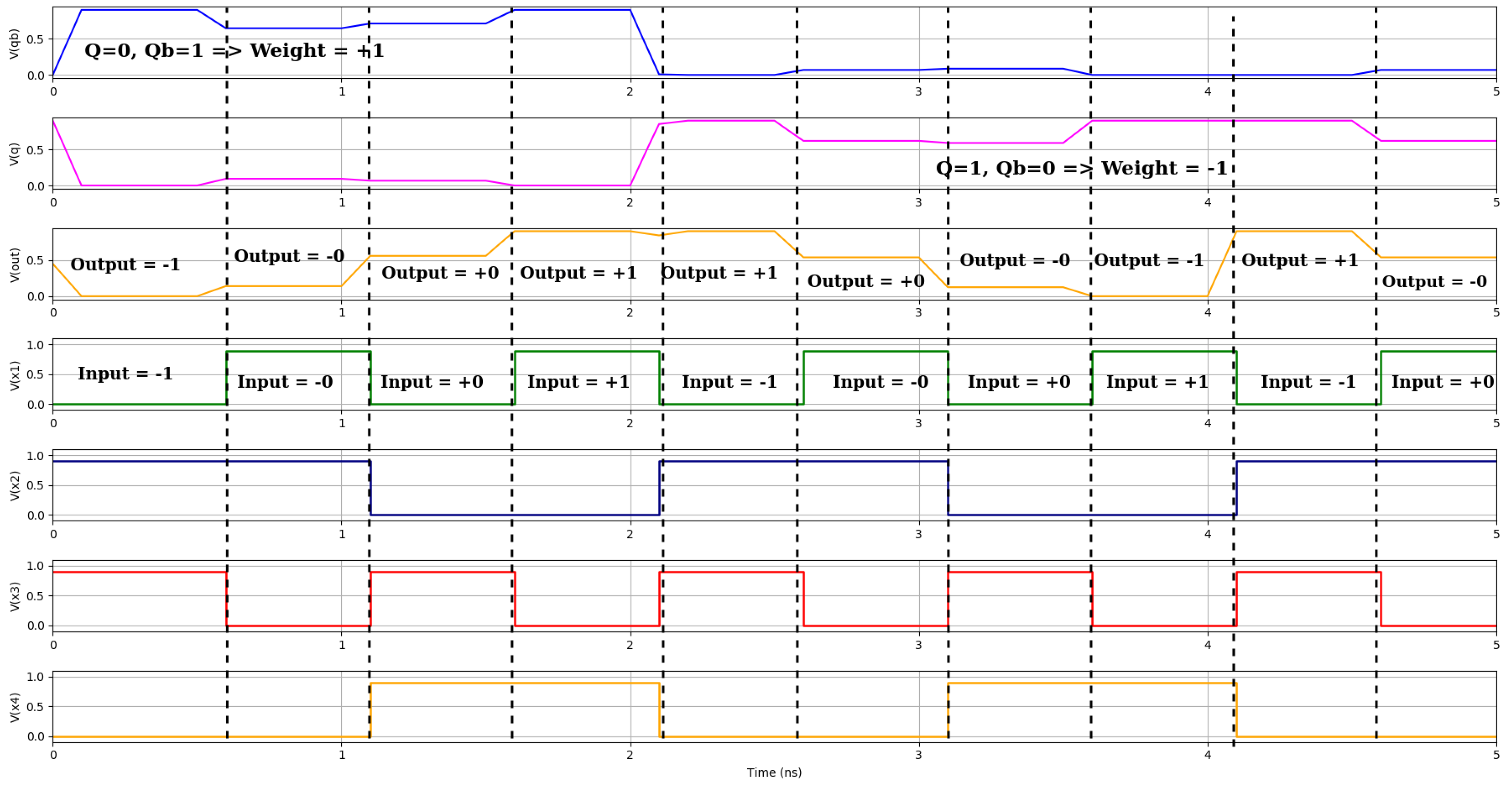
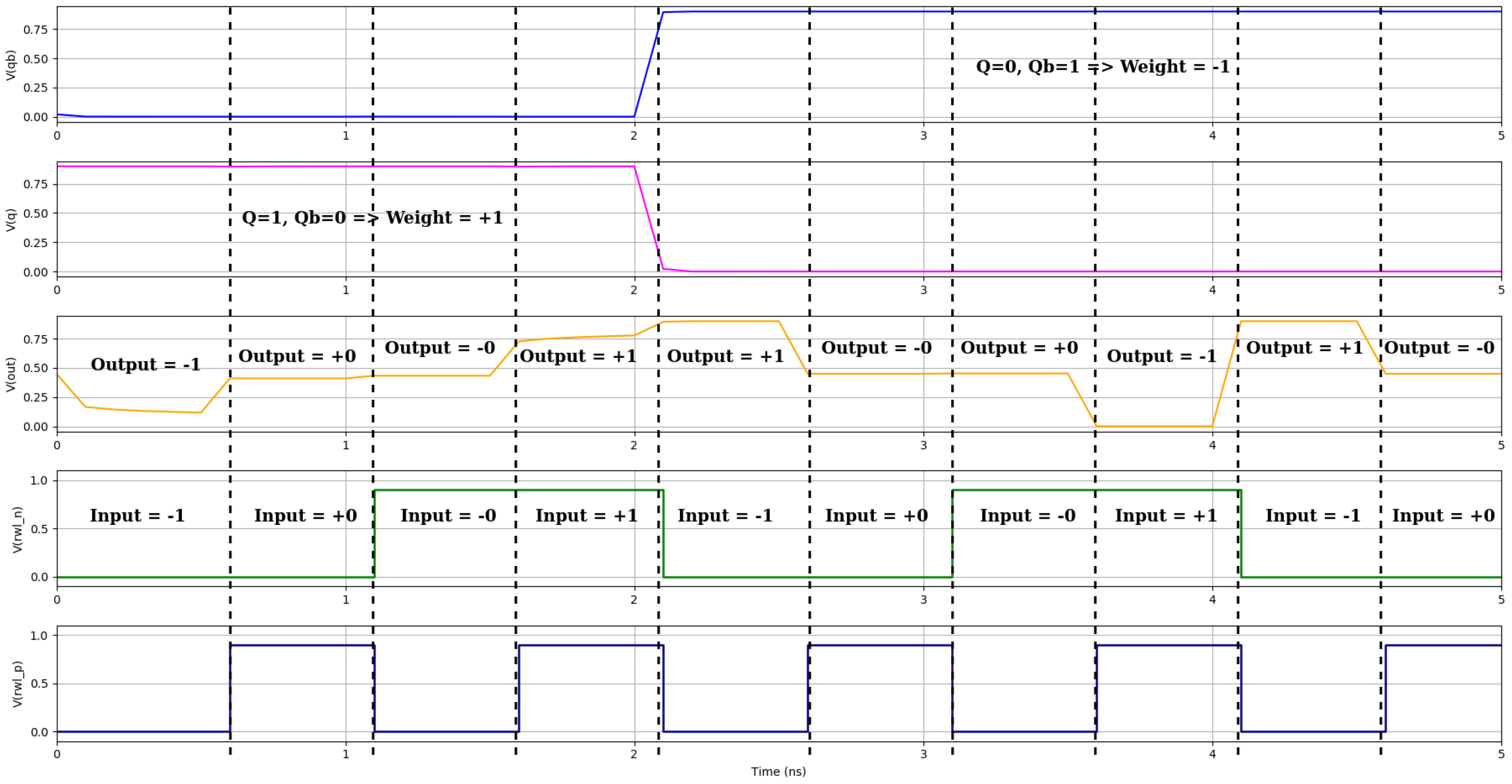
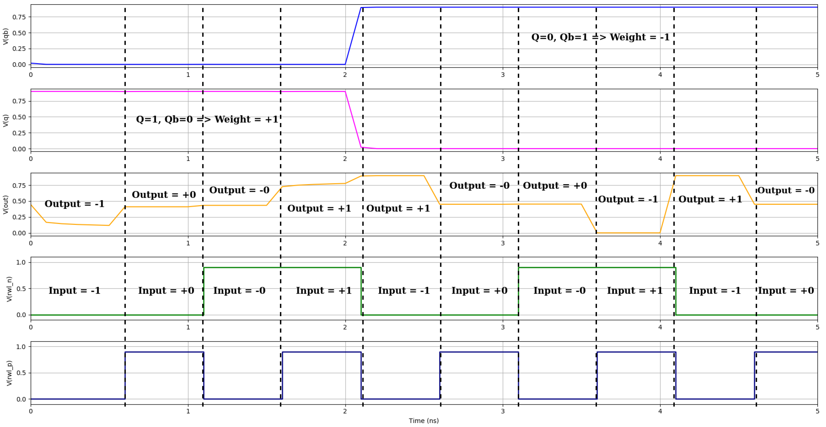
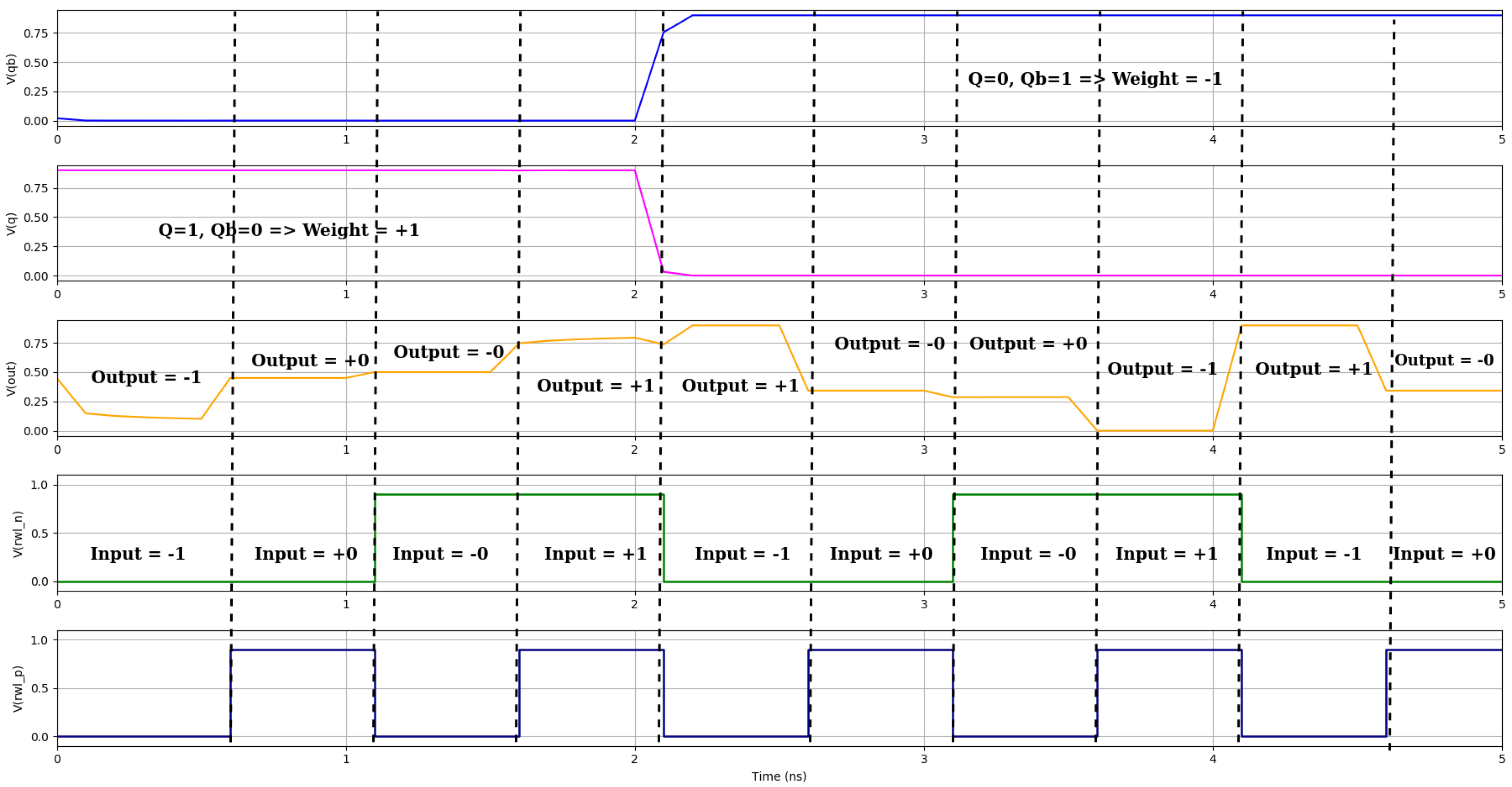
The following graphs display the output waveforms for the original SRAM design [
13] (
Figure 6), PLNA (
Figure 7), NLPA (
Figure 8), and SE (
Figure 9) when four input combinations and weights of +1 and −1 are used to simulate SRAM designs. The latency and power consumption of each design are assessed using these waveforms, which were created with Synopsys’ CosmosScope Waveform Analyzer 2012. The four input signals are identified by binary values (−1, −0, +0, and +1), each of which is linked to either +1 or −1 weights. Using FF corner at
0.80 V and
25 °C provides the best-case conditions for our design, resulting in minimal delay and reduced dynamic power consumption.
The comparative waveform analysis across the original, PLNA, NLPA, and SE SRAM designs reveals distinct differences in delay, stability, and power efficiency. The original XNOR-SRAM design [
13] correctly performs ternary computation but exhibits sharper transitions and higher switching activity, which contribute to increased power consumption. In contrast, the PLNA and NLPA designs exhibit smoother signal behavior and reduced transition noise, indicating improvements in both delay and overall energy efficiency.
From the results, it is evident that the PLNA structure achieves the most consistent signal transitions, producing stable outputs with lower glitching activity. This directly translates into reduced dynamic power consumption and faster convergence to the desired ternary values. The NLPA design also demonstrates accurate computation while offering a favorable balance between delay and stability, making it competitive for applications where energy efficiency is critical.
Meanwhile, the SE SRAM configuration further extends the efficiency improvements by producing the lowest observed power dissipation among the evaluated designs. Although its transitions are slightly less sharp than those of PLNA, the SE structure provides an optimized compromise between stability and power, ensuring reliable operation even under increased switching activity. This makes the SE variant particularly attractive for large-scale CIM arrays, where cumulative energy savings can be significant.
Taken together, these results reinforce the viability of the proposed CIM approach for ternary input processing. By leveraging variations of the XNOR-SRAM design—original, PLNA, NLPA, and SE—each architecture offers unique trade-offs between delay, stability, and power. Improvements observed in PLNA, NLPA, and SE implementations over the baseline design suggest that carefully chosen transistor-level optimizations can deliver substantial performance and energy benefits, paving the way for more scalable and efficient CIM-based computing platforms.
7. Conclusions
To optimize power delay performance, we propose a novel CIM structure in this study, created using FinFET 7nm technology. The CIM structure was implemented using three SRAM structures: P-Latch N-Access (PLNA), N-Latch P-Access (NLPA), and Single-Ended (SE) architectures. We contrasted these designs with an original 10T SRAM architecture across a variety of input–weight combinations using comprehensive simulations. In comparison to the original design, the SE architecture achieved a 74.89% reduction in power consumption, the PLNA architecture achieved a 70.82% reduction, and the NLPA architecture achieved a 64.39% reduction. The results show significant power reductions for all three systems. The PLNA design achieved the lowest overall delay (0.0111 ns), followed by the SE design (0.01163 ns), the NLPA design (0.013 ns), and the original design at 1.009 ns. All three PLNA, NLPA, and SE architectures also outperformed the original 10T SRAM design in terms of speed.
In conclusion, the suggested CIM structure significantly improves processing speed and power efficiency when simulated using PLNA, NLPA, and SE architectures. This study positions the PLNA, NLPA, and SE architectures as workable options for low-power, high-performance memory in sophisticated computer systems by highlighting the benefits of binary-weighted operations for power optimization. We are now developing a new ADC converter that transforms analog images into digital output. Then, we will utilize the CIM architecture proposed in this design to perform MAC operations on it.
Author Contributions
Conceptualization, data curation, formal analysis, investigation, methodology, validation, A.A.P. and S.S.D.; writing—original draft, writing—review and editing, A.G.; supervision, funding acquisition, project administration, K.K.C. All authors have read and agreed to the published version of the manuscript.
Funding
This work was supported by the Technology Innovation Program (20018906, Development of autonomous driving collaboration control platform for commercial and task assistance vehicles) funded by the Ministry of Trade, Industry and Energy (MOTIE, Republic of Korea).
Data Availability Statement
The data presented in this study are available on request from the corresponding author.
Acknowledgments
We thank our colleagues from KETI and KEIT, who provided insight and expertise, which greatly assisted the research and improved the manuscript.
Conflicts of Interest
The authors declare no conflicts of interest.
Abbreviations
The following abbreviations are used in this manuscript:
| AI | Artificial Intelligence |
| CNN | Convolution Neural Network |
| DNN | Deep Neural Network |
| PLNA | P-Latch N-Access |
| SE | Single-Ended |
| MAC | Multiply and Accumulate |
| SRAM | Static Random Access Memory |
| CIM | Compute-in-Memory |
| ADC | Analog-to-Digital Converter |
| TBN | Ternary Binary Neural Network |
References
- Hinton, G.; Deng, L.; Yu, D.; Dahl, G.E.; Mohamed, A.-R.; Jaitly, N.; Senior, A.; Vanhoucke, V.; Nguyen, P.; Sainath, T.N.; et al. Deep neural networks for acoustic modeling in speech recognition: The shared views of four research groups. IEEE Signal Process. Mag. 2012, 29, 82–97. [Google Scholar] [CrossRef]
- Taigman, Y.; Yang, M.; Ranzato, M.A.; Wolf, L. DeepFace: Closing the gap to human-level performance in face verification. In Proceedings of the 2014 IEEE Conference on Computer Vision and Pattern Recognition, Columbus, OH, USA, 23–28 June 2014; pp. 1701–1708. [Google Scholar] [CrossRef]
- Fang, W.; Wang, L.; Ren, P. Tinier-YOLO: A real-time object detection method for constrained environments. IEEE Access 2020, 8, 1935–1944. [Google Scholar] [CrossRef]
- Alemdar, H.; Leroy, V.; Prost-Boucle, A.; Pétrot, F. Ternary neural networks for resource-efficient AI applications. In Proceedings of the 2017 International Joint Conference on Neural Networks (IJCNN), Anchorage, AK, USA, 14–19 May 2017; pp. 2547–2554. [Google Scholar] [CrossRef]
- Song, T.; Jung, J.; Rim, W.; Kim, H. A 7nm FinFET SRAM using EUV lithography with dual write-driver-assist circuitry for low-voltage applications. In Proceedings of the 2018 IEEE International Solid-State Circuits Conference (ISSCC), San Francisco, CA, USA, 11–15 February 2018. [Google Scholar] [CrossRef]
- Lu, A.; Peng, X.; Luo, Y.; Yu, S. Benchmark of the compute-in-memory based DNN accelerator with area constraint. IEEE Trans. Very Large Scale Integr. (VLSI) Syst. 2020, 28, 1945–1952. [Google Scholar] [CrossRef]
- Si, X.; Khwa, W.-S.; Chen, J.-J.; Li, J.-F.; Sun, X.; Liu, R.; Yu, S.; Yamauchi, H.; Li, Q.; Chang, M.-F. A dual-split 6T SRAM-based computing-in-memory unit-macro with fully parallel product-sum operation for binarized DNN edge processors. IEEE Trans. Circuits Syst. I Regul. Pap. 2019, 66, 4172–4185. [Google Scholar] [CrossRef]
- Castro, V.D.; Marcos, E.; Vara, J.M. Applying CIM-to-PIM model transformations for the service-oriented development of information systems. Inf. Softw. Technol. 2010, 52, 1295–1311. [Google Scholar] [CrossRef]
- Alnatsheh, N.; Kim, Y.; Cho, J.; Choi, K.K. A Novel 8T XNOR-SRAM: Computing-in-Memory Design for Binary/Ternary Deep Neural Networks. Electronics 2023, 12, 877. [Google Scholar] [CrossRef]
- Kim, Y.; Patel, S.; Kim, H.; Yadav, N.; Choi, K.K. Ultra-Low Power and High-Throughput SRAM Design to Enhance AI Computing Ability in Autonomous Vehicles. Electronics 2021, 10, 256. [Google Scholar] [CrossRef]
- Kim, Y.; Li, S.; Yadav, N.; Choi, K.K. A Novel Ultra-Low Power 8T SRAM-Based Compute-in-Memory Design for Binary Neural Networks. Electronics 2021, 10, 2181. [Google Scholar] [CrossRef]
- Yadav, N.; Shah, A.P.; Vishvakarma, S.K. Stable, reliable, and bit-interleaving 12T SRAM for space applications: A device circuit co-design. IEEE Trans. Semicond. Manuf. 2017, 30, 276–284. [Google Scholar] [CrossRef]
- Lee, S.; Kim, Y. Low power ternary XNOR using 10T SRAM for in-memory computing. In Proceedings of the 2022 19th International SoC Design Conference (ISOCC), Gangneung-si, Republic of Korea, 19–22 October 2022; pp. 352–353. [Google Scholar] [CrossRef]
- Yin, S.; Jiang, Z.; Seo, J.-S.; Seok, M. XNOR-SRAM: In-memory computing SRAM macro for binary/ternary deep neural networks. IEEE J. Solid-State Circuits 2020, 55, 1733–1743. [Google Scholar] [CrossRef]
- Biswas, A.; Chandrakasan, A.P. CONV-SRAM: An energy-efficient SRAM with in-memory dot-product computation for low-power convolutional neural networks. IEEE J. Solid-State Circuits 2019, 54, 217–230. [Google Scholar] [CrossRef]
- Almeida, R.B.; Marques, C.; Butzen, P.F.; Silva, F.; Reis, R.A.; Meinhardt, C. Analysis of 6T SRAM cell in sub-45 nm CMOS and FinFET technologies. Microelectron. Reliab. 2018, 88, 196–202. [Google Scholar] [CrossRef]
- Vangala, M.; Clark, L.T.; Brunhaver, J.S.; Allee, D.R. FinFET Cell Library Design and Characterization. 2017. Available online: https://hdl.handle.net/2286/R.I.45536 (accessed on 17 September 2025).
- Narasimham, B.; Luk, H.; Paone, C.; Montoya, A.R.; Riehle, T.; Smith, M.; Tsau, L. Scaling trends and the effect of process variations on the soft error rate of advanced FinFET SRAMs. In Proceedings of the 2023 IEEE International Reliability Physics Symposium (IRPS), Monterey, CA, USA, 26–30 March 2023; pp. 1–4. [Google Scholar] [CrossRef]
- Jeong, H.; Kim, S.; Park, K.; Jung, J.; Lee, K.J. A Ternary Neural Network Computing-in-Memory Processor with 16T1C Bitcell Architecture. IEEE Trans. Circuits Syst. II Express Briefs 2023, 70, 1739–1743. [Google Scholar] [CrossRef]
Figure 1.
Compute-In-Memory (CIM) architecture for efficient image processing using in-memory MAC operations.
Figure 1.
Compute-In-Memory (CIM) architecture for efficient image processing using in-memory MAC operations.
Figure 2.
Pass transistor logic.
Figure 2.
Pass transistor logic.
Figure 3.
P-Latch N-Access (PLNA) SRAM structure with XNOR logic.
Figure 3.
P-Latch N-Access (PLNA) SRAM structure with XNOR logic.
Figure 4.
N-Latch P-Access (NLPA) SRAM structure with XNOR logic.
Figure 4.
N-Latch P-Access (NLPA) SRAM structure with XNOR logic.
Figure 5.
Single-Ended (SE) SRAM structure with XNOR logic.
Figure 5.
Single-Ended (SE) SRAM structure with XNOR logic.
Figure 6.
The above waveform represents the CIM operation output for the SRAM circuit in [
13], illustrating the XNOR-SRAM CIM operation with ternary inputs. Cyan, magenta, black, and yellow lines represent the input signals (+1, 0, −1, +0), while the orange line shows the ternary output (−1, 0, +1). The blue and green lines correspond to Q and Qb, respectively, confirming correct ternary computation through XNOR pass transistor logic.
Figure 7.
The PLNA SRAM waveform illustrates the XNOR-SRAM CIM operation for ternary inputs. Input levels (+1, −1, +0, −0) are represented by green and blue signals, with the ternary output shown in orange. The weights (+1,−1) are represented by Q and Qb and are marked in pink and blue, respectively, and the output (rbl) is represented in yellow.
Figure 8.
The suggested XNOR-SRAM CIM operation for ternary inputs is analyzed using NLPA SRAM waveforms. Green and blue, respectively, indicate the input signals (+1, −1, +0, −0). The orange line displays the ternary combination output (−1, 0, +1). The pink line represents the primary output Q, and the blue line indicates the complementary output Qb. Correct ternary computation is demonstrated by the results.
Figure 9.
The suggested XNOR-SRAM CIM operation for ternary inputs is analyzed using SE SRAM waveforms. Green and blue, respectively, indicate the input signals (+1, −1, +0, −0). The orange line displays the ternary combination output (−1, 0, +1). The pink line represents the primary output Q, and the blue line indicates the complementary output Qb. Correct ternary computation is demonstrated by the results.
Table 1.
Logic diagram for the product of the weight and the input.
Table 1.
Logic diagram for the product of the weight and the input.
| Input Value | Inputs | Weights | Weight Value | RBL |
|---|
|
RWL_P
|
RWL_N
|
Q
|
Q_b
|
|---|
| −1 | 0 | 0 | 1 | 0 | +1 | −1 |
| −0 | 0 | 1 | 1 | 0 | +1 | 0 |
| +0 | 1 | 0 | 1 | 0 | +1 | 0 |
| +1 | 1 | 1 | 1 | 0 | +1 | 1 |
| −1 | 0 | 0 | 0 | 1 | −1 | 1 |
| −0 | 0 | 1 | 0 | 1 | −1 | 0 |
| +0 | 1 | 0 | 0 | 1 | −1 | 0 |
| +1 | 1 | 1 | 0 | 1 | −1 | −1 |
Table 2.
Transistor sizing for FinFET in PLNA 6T SRAM cell.
Table 2.
Transistor sizing for FinFET in PLNA 6T SRAM cell.
| Number | Transistor | Number of FINs |
|---|
| 1 | M1 | 1 |
| 2 | M2 | 1 |
| 3 | M3 | 2 |
| 4 | M4 | 2 |
| 5 | M5 | 4 |
| 6 | M6 | 8 |
Table 3.
Transistor sizing for FinFET in NLPA 6T SRAM cell.
Table 3.
Transistor sizing for FinFET in NLPA 6T SRAM cell.
| Number | Transistor | Number of FINs |
|---|
| 1 | M1 | 2 |
| 2 | M2 | 2 |
| 3 | M3 | 4 |
| 4 | M4 | 4 |
| 5 | M5 | 4 |
| 6 | M6 | 8 |
Table 4.
Transistor sizing for FinFET in SE 6T SRAM cell.
Table 4.
Transistor sizing for FinFET in SE 6T SRAM cell.
| Number | Transistor | Number of FINS |
|---|
| 1 | M1 | 1 |
| 2 | M2 | 1 |
| 3 | M3 | 2 |
| 4 | M4 | 2 |
| 5 | M5 | 4 |
| 6 | M6 | 8 |
Table 5.
Comparison of FinFET PLNA, FinFET NLPA, and FinFET SE configurations’ power consumption for various weights and inputs.
Table 5.
Comparison of FinFET PLNA, FinFET NLPA, and FinFET SE configurations’ power consumption for various weights and inputs.
| Weight | Input | RBL | Power (μW) |
|---|
|
Original [13]
|
FinFET PLNA
|
FinFET NLPA
|
FinFET SE
|
|---|
| +1 (1, 0) | (−1) | Discharge | 2.579 | 0.268 | 0.261 | 0.271 |
| +1 (1, 0) | (+0) | Stable | 189.860 | 87.060 | 92.350 | 61.440 |
| +1 (1, 0) | (−0) | Stable | 118.210 | 0.655 | 0.528 | 0.622 |
| +1 (1, 0) | (+1) | Charge | 23.300 | 0.188 | 0.153 | 0.140 |
| −1 (0, 1) | (−1) | Charge | 1.885 | 0.07 | 0.0130 | 0.085 |
| −1 (0, 1) | (+0) | Stable | 119.530 | 99.030 | 134.800 | 94.680 |
| −1 (0, 1) | (−0) | Stable | 185.600 | 0.782 | 0.957 | 0.742 |
| −1 (0, 1) | (+1) | Discharge | 6.611 | 0.159 | 0.594 | 0.090 |
Table 6.
Overall power comparison of FinFET designs.
Table 6.
Overall power comparison of FinFET designs.
| Design | Total Power (μW) | Difference (μW) | Percentage Reduction (%) |
|---|
| FINFET Original [13] | 81.401 | - | - |
| FINFET PLNA | 23.76 | 57.641 | 70.82% |
| FINFET NLPA | 28.98 | 52.421 | 64.39% |
| FINFET SE | 20.49 | 60.911 | 74.89% |
Table 7.
Overall delay comparison.
Table 7.
Overall delay comparison.
| Design | Total Delay |
|---|
| Original [13] | 1.009 ns |
| PLNA | 0.0111 ns |
| NLPA | 0.0130 ns |
| SE | 0.0116 ns |
Table 8.
Delay comparison for different operations.
Table 8.
Delay comparison for different operations.
| Operation | Original [13] (pS) | PLNA (pS) | NLPA (pS) | SE (pS) |
|---|
| 23.77 | 1.008 | 0.959 | 1.006 |
| 20.652 | 0.509 | 1.501 | 0.508 |
| 20.57 | 2.506 | 3.006 | 3.008 |
| 21.22 | 1.504 | 1.505 | 1.505 |
| Disclaimer/Publisher’s Note: The statements, opinions and data contained in all publications are solely those of the individual author(s) and contributor(s) and not of MDPI and/or the editor(s). MDPI and/or the editor(s) disclaim responsibility for any injury to people or property resulting from any ideas, methods, instructions or products referred to in the content. |
© 2025 by the authors. Licensee MDPI, Basel, Switzerland. This article is an open access article distributed under the terms and conditions of the Creative Commons Attribution (CC BY) license (https://creativecommons.org/licenses/by/4.0/).
