Article

Output Filtering Capacitor Bank Monitoring for a DC–DC Buck Converter

by
Dadiana-Valeria Căiman
*,
Corneliu Bărbulescu
,
Sorin Nanu
and
Toma-Leonida Dragomir
Faculty of Automation and Computer Since, Politehnica University Timișoara, 2 Vasile Pârvan, Bd., 300223 Timișoara, Romania
*
Author to whom correspondence should be addressed.
Electronics 2025, 14(18), 3614; https://doi.org/10.3390/electronics14183614 (registering DOI)
Submission received: 9 August 2025 / Revised: 6 September 2025 / Accepted: 10 September 2025 / Published: 11 September 2025
(This article belongs to the Special Issue New Insights in Power Electronics: Prospects and Challenges)

Abstract

The remote prognostic, diagnosis, and maintenance of electrolytic capacitors are research topics of interest due to their presence in numerous electronic devices and their increased susceptibility to degradation over time. The authors’ focus in this article is on the proposal of a new diagram for monitoring the parameters of the capacitors that compose the filter bank of a DC–DC buck converter by connecting them in parallel. Each capacitor is modeled by an equivalent series R–C circuit composed of an equivalent capacitance and an equivalent series resistance (ESR). The method used allows successive investigation of the three capacitors that compose the bank by triggering discharge/charge sequences, acquiring the voltages at the capacitor terminals, and estimating the time constants of each capacitor using a parameter observer. During the estimation of the parameters of a capacitor, the converter uses the other two capacitors maintained in operation. The monitoring cycle of all capacitors of the bank lasts less than  40   m s , not significantly affecting the operation of the converter. The study undertaken is correlated with the thermal map of the board on which the converter is made. The dispersion of the measured values of the equivalent capacitances is below  0.25 % , and of the ESR below  2.6 % . The major advantage of the method is that the monitoring is performed online and in real time.

1. Introduction

The important role of electronic equipment, in particular power electronic converters, requires monitoring the health and condition of the equipment and/or of the corresponding components. This also entails monitoring filter capacitors and converters. Both the diagnosis and prognosis of the condition of capacitors are of interest. The diagnosis signals the failure of a capacitor and, potentially, of the converter. The prognosis provides information about the capacitor’s remaining useful lifetime (RUL) and, implicitly, about the stability of the converter operation [1,2]. As such, the remote prognosis, diagnosis, and maintenance represent a goal for real-world applications [3] that require methods of real-time monitoring capacitors by operating conditions [4], in an online or at least quasi-online regime.
To assess the capacitors’ ability to perform various functions in electronic converters, in particular the filtering function, the most frequently used model is the R–C series model, with R representing the equivalent serial resistance of the capacitor, denoted in the article by  R s e , and C representing its capacitance, denoted by    C e . In applications, electrolytic capacitor degradation thresholds are 200% of the R value and/or 80% of the C value compared to the nominal/initial values [5]. Subsequently, the values of R and C should be regarded as diagnostic parameters, either individually or collectively. Many papers focused on monitoring individual capacitors rely on the value of R as a diagnostic parameter. The use of only the value of C as a diagnosis parameter has also been considered in [6,7]. In some cases, such as the case of metalized film capacitors, with the ESR values being very low [8,9], only the value of C is used to monitor the health of capacitors. The literature reports a lot of research that proposes methods for determining capacitor parameters. The main categories of methods are based on the investigation of the current or voltage ripple of the capacitor in steady state operation, on the investigation of induced transient regimes, of capacitor discharge and/or charging, and on the investigation of the capacitor behavior under the injection of external signals [10,11,12].
Depending on the capacitor’s operating mode during the estimation, the estimated values are associated with different ranges of frequencies, which, on the one hand, makes it difficult to compare the methods and on the other hand, requires operations to adapt the estimated values to real-world conditions. Finally, from a practical point of view, online methods applicable in real time that use minimum sensors and that perform the estimation in the shortest time possible are of primary interest.
The estimations of capacitor parameters in power converters are affected by the errors introduced by the methods of acquisition of the measured signals, the estimation methods, and by the failure to meet the validity assumptions of the estimation methods (e.g., the accuracy of modeling/characterization of the components, the constancy of the operating temperature of the converters, etc.). The precision of the estimates also depends on many other factors, mainly on the amplitude and spectrum of the measured signals, the signal-to-noise ratio, and the characteristics of the converter load. It is important to mention that these aspects, although analyzed and discussed in numerous papers, were obtained mainly under laboratory conditions. As we limit ourselves only to the influence of temperature on capacitor behavior, it is obvious that the estimation accuracy of the proposed methods also suffers, because the temperature value cannot be determined exactly [10]. Numerous studies highlight based on experiments that as the capacitor temperature increases,  C e  increases and  R s e  decreases. Also, with the increase in the fundamental frequency of the voltage at the capacitor terminals, the frequency characteristics of  C e  and  R s e  fall [13]. These variations are synthesized through mathematical models. Regarding applications related to filter capacitors, [14] shows that, until 2018, research was predominantly focused on filters made with a single capacitor. The paper emphasizes that since the capacitors in a bank are not identical, it is necessary to monitor the capacitors of a bank individually and not only the bank. At the same time, [14] mentions that the more sensors are used for monitoring, the more the converter operation is distorted. Subsequent research related to capacitor banks is scarce. The replacement of a single capacitor with capacitor banks in power electronics applications primarily aims to increase the reliability of the capacitive block (arrangement) [15]. However, the article [16] notes that in the field of photovoltaic applications, most of the studies are dedicated to evaluating the reliability of single-capacitor schemes, specifically the one at the DC interface of the PV inverter, based on the research [12,14,17,18,19,20,21,22,23,24]. Table A1 in Appendix A presents a synthesis in the context of these aspects.
Among the capacitor condition monitoring methods, there are also methods that use state observers [25,26,27]. Depending on the case, the observers are associated with the entire output circuit of the converters or only parts of it. In [28], a new type of observer, called a parameter observer (PO), is implemented. Its role is to determine the time constant of the filter capacitor discharge circuits and to calculate, based on their values, the equivalent parameters  C e  and  R s e . The adaptation of PO to discharge/charge processes led to the parameter observer on two edges (PO2) [29].
The present paper continues the research from [30] by presenting a possibility of estimating the equivalent parameters of several capacitors connected in parallel to form the output filter of a DC–DC buck converter. From the point of view of the signal profile acquired to estimate the capacitor parameters, the presented diagram corresponds to principle II proposed in [10], i.e., non-periodic charging/discharging large signal. The non-periodic large signals appear in the transient regimes generated by switches that interconnect the basic configuration of the converter with a variable electrical network (VEN). VEN consists of resistors through which the filter capacitor discharges/charges. The acquired signal is the voltage at the evaluated capacitor terminals. The values of the equivalent parameters of each capacitor are obtained by a PO2 implemented on a microcontroller monitoring the corresponding voltage. The experiments were performed on a DC–DC buck–boost converter based on a dedicated integrated circuit (LTC3780). Since the proposed scheme has only the goal of estimating the values of the capacitor parameters, which represents only part of the converter’s maintenance strategy, the microcontroller implicitly also has the task of transmitting the estimated values to the higher level of the implemented maintenance strategy.
The main contribution of the paper consists of the proposed method, namely, the implementation of the monitoring of the parameters of a DC–DC buck converter filter bank capacitors. These differ from the diagrams in [29] by combining the discharge/charge processes from which the equivalent parameters of the bank capacitors result. The consequence was a considerable reduction in the duration of the cycle of estimation of all capacitors. The estimation is performed online, in real time, without the use of sensors. The results of the experiments are discussed in the context of the thermal map of the converter used.
Section 2 briefly presents the theoretical support for calculating the equivalent parameters of the capacitors in the output filter and its implementation method for a DC–DC buck converter. Section 3 details both the circuit used and the experimental results obtained. Section 4 analyzes the experimental results. Section 5, the last one, summarizes the conclusions of the article.

2. Materials and Methods

2.1. The Principle of Estimating the Values of the Equivalent Parameters of a Capacitor Modeled by a Series R–C Circuit

Consider the circuit in Figure 1a with the capacitor initially charged. By selecting the switch position 1 or 2, the capacitor will discharge across the resistors  R 1  or  R 2 , the discharge circuits having, respectively, the time constants:
T 1 = R 1 + R s e · C e ,       T 2 = R 2 + R s e · C e
Considering  T 1 T 2 R 1 R 2  known, equalities (1) allow the calculation of the equivalent parameters  R s e  and  C e . Equation (1) is also valid for the circuit in Figure 1b, in which the capacitor is charged through  R 2  from a source that supplies the constant DC voltage  v  and then discharged across  R 1 .
According to [29   T 1  and  T 2  can be estimated in real time from the signals  v C ( t )  generated during the capacitor discharges and charges using a parameter observer (PO). Denoting by  T ^ 1  and  T ^ 2  the estimates of the time constants, the estimates of the equivalent capacitor parameters are obtained by Formulas (2):
R ^ s e = T ^ 2 · R 1 T ^ 1 · R 2 T ^ 1 T ^ 2 ,       C ^ e = T ^ 1 T ^ 2 R 1 R 2   .
The principle of estimating the parameters of the filter capacitors of the converter that is the subject of the present study corresponds to the discharge/charge process in Figure 1b. From a systemic point of view, this is a process with a variable structure. The circuit in Figure 1b represents a master system (MS) whose output signal  v C ( t )  is processed by PO2.
According to Figure 2a, PO2 contains a PO capable of estimating T only for a discharge signal  v C ( t ) , and an adapter (AD). When a discharge process occurs in the MS, the adapter provides the signal  y t = v C ( t ) , and when a charging process occurs, it provides  y t = K v C ( t ) , where K is the value of the capacitor supply voltage  v ( t ) = K , and the limit value  K = lim t   v C ( t ) . In Figure 2b, a discharge/charge process, hereafter called a sequence, is shown, which highlights this limit. The adapter switching to one of the two expressions of  y ( t )  is synchronized by an external command with the discharge/charge processes in the MS (see the blue command line in Figure 2a).
PO2 is the second-order discrete-time tracking system (3) that processes the samples  v C k = v C ( k h )  of  v C ( t )  acquired with the sampling step  h  [4].
O 2 :   I A v S : y k = v C k , f o r   a   d i s c h a r g i n g   p h a s e K v C k ,   f o r   a   c h a r g i n g   p h a s e   , P O : z k = ln y k , z ^ k = z ^ k 1 + h · c ^ k ,     z ^ 0 = z ^ o , ε k = z k z ^ k , c ^ k = K p · ε k ε k 1 + h · K i · ε k 1 + c ^ k 1 ,       c ^ 0 = c ^ o ,   T ^ k = 1 c ^ k ,
The parameters  K p  and  K i  in (3) are calculated with Formulas (4) depending on the length τ of the time interval after which it is desired to reach the tracking regime. In (4),  ω o  is chosen so that  τ · ω o 10 .
K p = 2 · ω 0 ,   K i = ω 0 2
PO2 completes the calculation of the time constant when condition (5) is met and the current value  T ^ k  is assigned to the estimated  T ^  value. In Equation (5),  k 0  is the value of k when the calculation is started.
T ^ k α · k k 0 ,   α = 2.5 .
In practical applications, the presented principle is implemented by including the  R 1 - R 2  resistors and the switches in a VEN controlled by a microcontroller, able to measure the voltage  v C ( t )  and run the PO2 algorithm.

2.2. Basic Electrical Diagram for Estimating the Equivalent Parameters of the Capacitors That Make up the Output Filter of a DC–DC Buck Converter

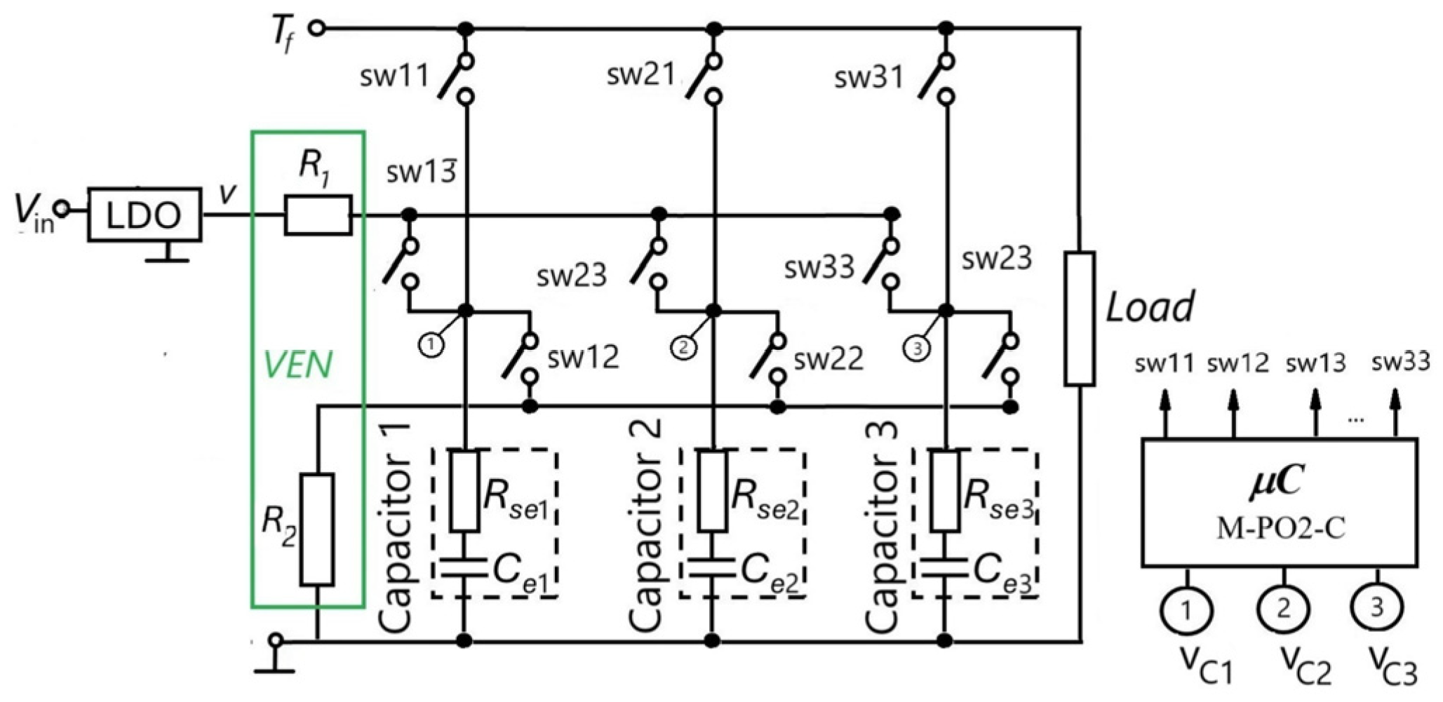
To apply the principle in Figure 2b, we propose the diagram in Figure 3. It can be extended to banks with more than three capacitors. The diagram allows for estimating the equivalent parameters  C e i R s e i i = 1 , 3 ¯  of the parallel-connected capacitor bank, Capacitor 1-Capacitor 2-Capacitor 3, of a buck DC–DC converter. The  T f  terminal is connected to the converter. The stabilized voltage source LDO provides the voltage  v . The microcontroller measures the voltages  v C i  at the terminals ➀, ➁, ➂, implements PO2 and controls the 9 switches sw11, …, sw33. These operations are symbolized by the notation M-PO2-C.
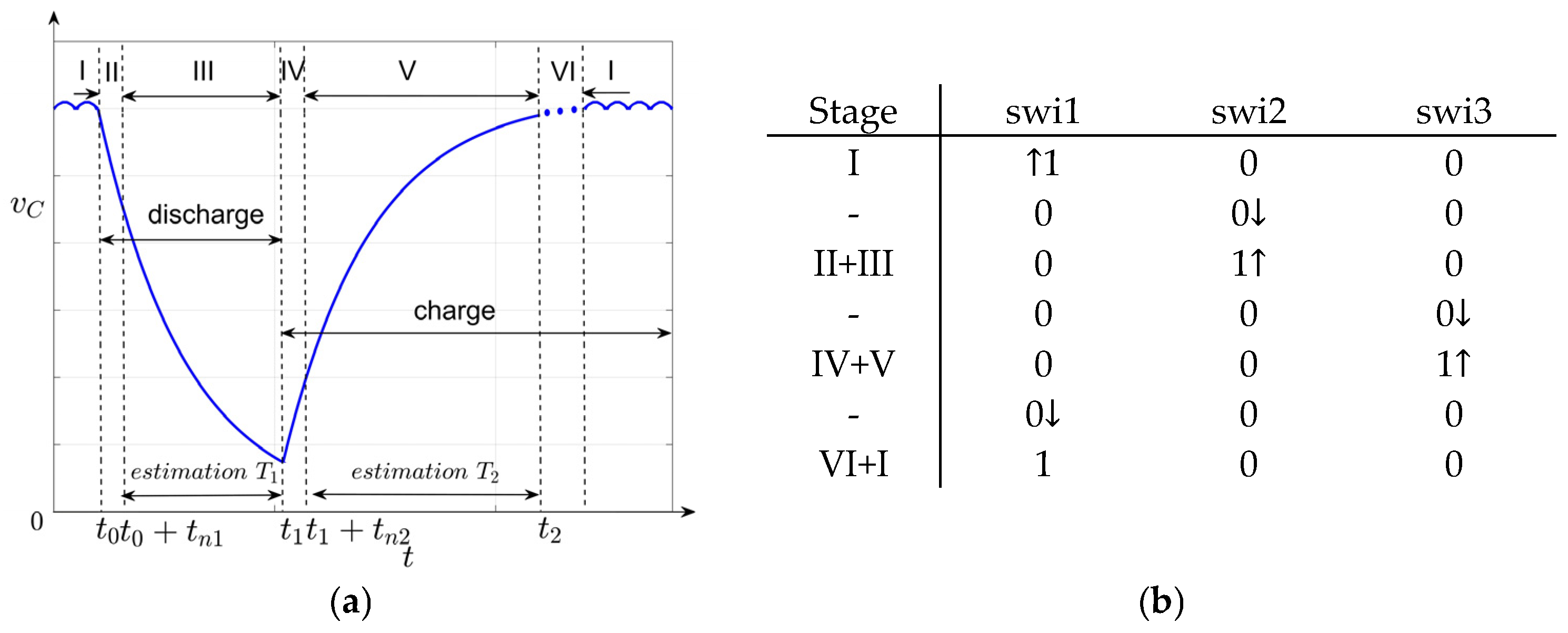
The monitoring of the three capacitors is performed sequentially by estimating the equivalent parameters during an estimation cycle with duration  t c . During the cycle, the parameters of each capacitor are successively evaluated when disconnected from the load, and the output filter is operating with the other two remaining capacitors. The evaluation of the parameters of a capacitor includes a sequence of discharge through R1/charge through R2. With the notations in Figure 2, the duration of an estimation sequence  i ,   i = 1 , 3 ¯  is  t 2 i t 0 i , and the duration of a cycle is  t c = i = 1 3 t 2 i t 0 i + 2 , where ∆ is the time interval between two consecutive sequences.
To reduce estimation errors, the sizing of the resistor pair  ( R 1 , R 2 )  in the VEN composition must comply with the following requirements [30]: (i) the value of the ratios  R s e i / R 2 i = 1 , 3 ¯  should be as close as possible to 1; and (ii)  R 1 R 2 . At the same time, the charging time interval must allow, together with the sampling rate, for obtaining a sufficiently large number of samples of the measured voltages  v C i , i = 1 , 3 ¯  for PO2 to complete the estimation.
In Figure 4a, the stages of an estimation sequence are detailed at the level of the measured voltage  v C t . Stage I corresponds to the normal DC–DC operating mode. In stage II the capacitor is isolated from the DC–DC converter, and its discharge can be triggered resulting in a transient regime during the whole stage. In stage III, the estimation of the time constant  T 1  is performed. The recharging is triggered in stage IV characterized by a similar transient regime followed by stage V where the estimation of the time constant  T 2  is processed and finished at its end. In stage VI, the charging continues up to the output voltage level of the converter making it possible to reconnect the capacitor to the bank for filtering and operating in DC–DC mode. Figure 4b shows the states of the switches in the different stages and the way in which one passes from one stage to another through them. The symbols used for the states, the respective commands are 1—closed, 0—open, respectively, ↑—open, ↓—close.
The diagram in Figure 3 extends the list of the four principal diagrams presented in [30], intended for estimating the equivalent parameters associated with the capacitors of the output filter of a converter. Table 1 presents a characterization of the four diagrams, as well as the one proposed in this paper (last column). The meaning of the Ids is specified in Table 2. The diagrams are indicated by the number of the figures in [30], respectively, by the figure in this article.
Compared to the most complex solution in [29] (fourth column), the main novelty of the proposed solution, highlighted in the table by the positions marked with (*) and (**), respectively, can be summarized as follows: To monitor the parameters of a capacitor, the scheme in [29] uses two discharge/charge sequences, unlike the scheme in Figure 3, which uses a single sequence. By reducing the number of sequences, the duration of estimating the parameters of a capacitor becomes much shorter than in [29]. Both schemes operate continuously, and the greater the number of capacitors in the bank, the greater the reliability of equivalent bank capacitance.

3. DC–DC Buck Converter Based on the Proposed Principle Diagram

3.1. Implementation

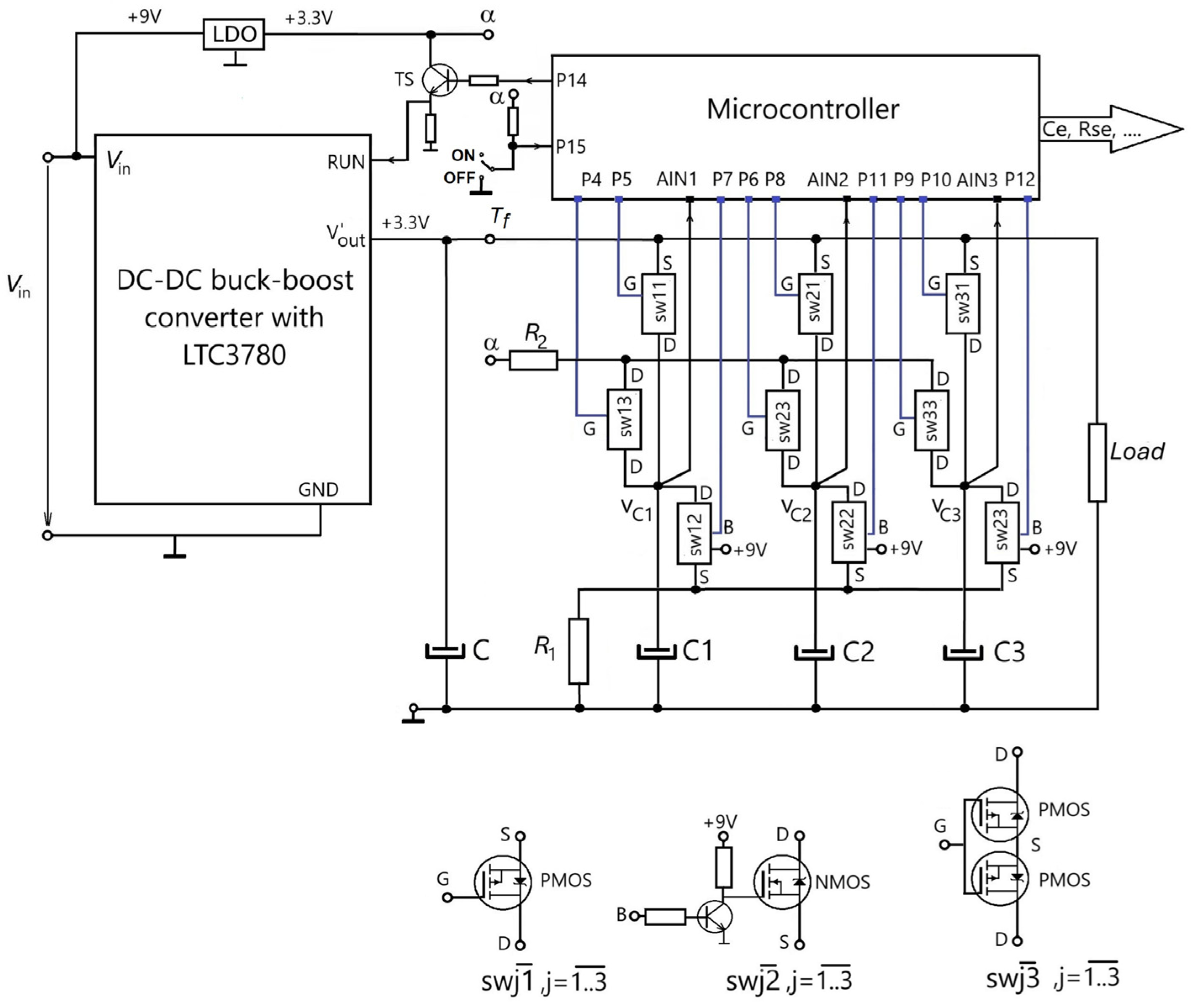
The implementation of the principle diagram in Figure 3 is illustrated by the structure in Figure 5 for a DC–DC buck-boost converter based on the LTC 3780 dedicated integrated circuit working in buck mode [30]. The diagram also includes a microcontroller, a Low Dropout Regulator (LDO), the VEN components (switches sw11, …, sw33 made with MOSFET transistors and resistors R1 and R2), and the TS stage, which ensures that the circuit is always started with the full capacity of the bank. The acquisition of the voltages  v C 1 v C 2  and  v C 3  is performed as in [28], through an application program running with an oversampling period of  2.5   μ s  and an equivalent sampling period  h   =   20   μ s . The microcontroller also ensures the external transmission of the capacitor parameter values for use in estimating the RUL of the capacitors or the converter.
The LTC 3780 integrated circuit allows three operating modes: buck if  V o u t V i n , boost if  V o u t V i n , and buck-boost if  V o u t V i n . In the present case, the evaluation of the capacitors was carried out in buck mode with  V i n = 9   V , respectively,  V o u t = 3.3   V . The output filtering bank capacitors consist of three 330 μF/35 V aluminum electrolytic capacitors  C i , i = 1 , 3 ¯  targeted in the evaluation process, and one 100 nF/40 V ceramic capacitor C. The set of MOSFET transistors ensures the necessary switching during the estimation cycle—T-swi1 allows the disconnection/connection of the evaluated capacitor from the converter, T-swi2 ensures the discharge of the capacitor over R1 = 90 Ω in order to estimate the time constant  T i 1 , and T-swi3 charges the capacitor from the LDO through R2 = 3.3 Ω, in order to estimate the time constant  T i 2 . A Teensy 4.0 development board containing an ARM Cortex-M7 microcontroller running at 600 MHz [31] is used as a control, acquisition, processing, and storage data unit. The structure of the program used to monitor the equivalent parameters of the converter output filter capacitors is presented in Figure 6.
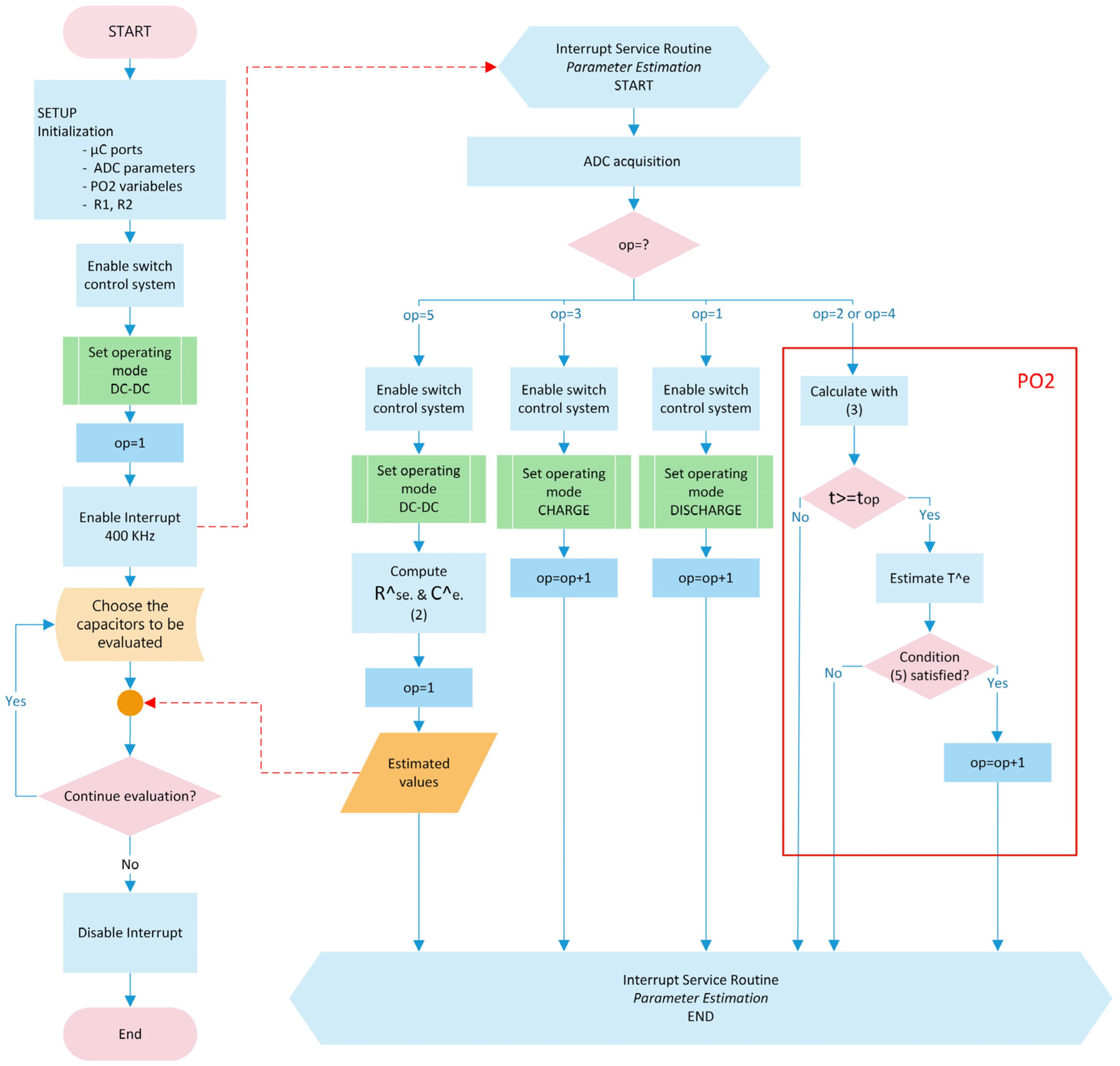
The flowchart is organized in two branches: the main flow and the interruption routine. It describes the algorithm for calculating the estimates of the equivalent parameters  C ^ e i  and  R ^ s e i i = 1 , 3 ¯ . The calculation is carried out using Equation (2), whose application requires a prior estimate of the time constants  T ^ 1 i , i = 1 , 3 ¯  for discharging over resistor  R 1 , and  T ^ 2 i , i = 1 , 3 ¯  for charging through resistor  R 2 . Time constants are estimated using Equation (3). The estimation of a time constant is completed when condition (5) is met. The primary branch of the flowchart starts with setup operations, which involve initializing the microcontroller ports, ADC parameters, and PO2 parameters. This is followed by setting the converter operating mode, initializing the op variable and enabling the interrupt ( 400   k H z ) routine where the estimates of  T ^ 1 i T ^ 2 i  based on algorithm (3) and the calculation of  C ^ e i  și  R ^ s e i  are implemented. Following the completion of all calculations, the op variable is reset, and the interrupts are disabled. The interrupt handling routine implements a sequence of estimating the parameters of a capacitor according to Figure 4. The op variable tracks the stages I, II, …, V, with the values  o p   =   1 o p   =   2 , …,  o p   =   5  being updated at the end of each stage. If the value of  o p    is 1 or 3, the switches of the evaluated capacitor are set according to the charge/discharge routine as specified in Figure 4b. In case of  o p   =   2  or 4 the PO2 block of the routine is triggered. In this sequence, the  t o p  is appropriately set as  t 2  and  t 4 , matching the moments  t 0 + t n 1  and  t 1 + t n 2  in Figure 4. As a result of this sequence, time constants are estimated. The last step of the interruption,  o p   =   5 , sets the switches to normal operation mode and calculates the equivalent parameters  C ^ e i  and  R ^ s e i , based on the time constants. The conditional block in the main branch enables the selection of the number of capacitors to be evaluated. “Choose the capacitors to be evaluated” block allows setting seven configurations for estimation: C1, C2, C3, C1 + C2, …, C1 + C2 + C3.
In case of monitoring cycles for only one or two capacitors, the operator will manage the operations of assigning the values of the variable  o p .
Figure 7 displays the frequency characteristics of the bank capacitors C1, C2, and C3 from Figure 5 obtained with a BK Precision RLC-bridge set for the serial capacitor model. In terms of C(f) and Rs(f) characteristics, some differences can be noticed, while the Z(f) characteristics are almost superimposed.
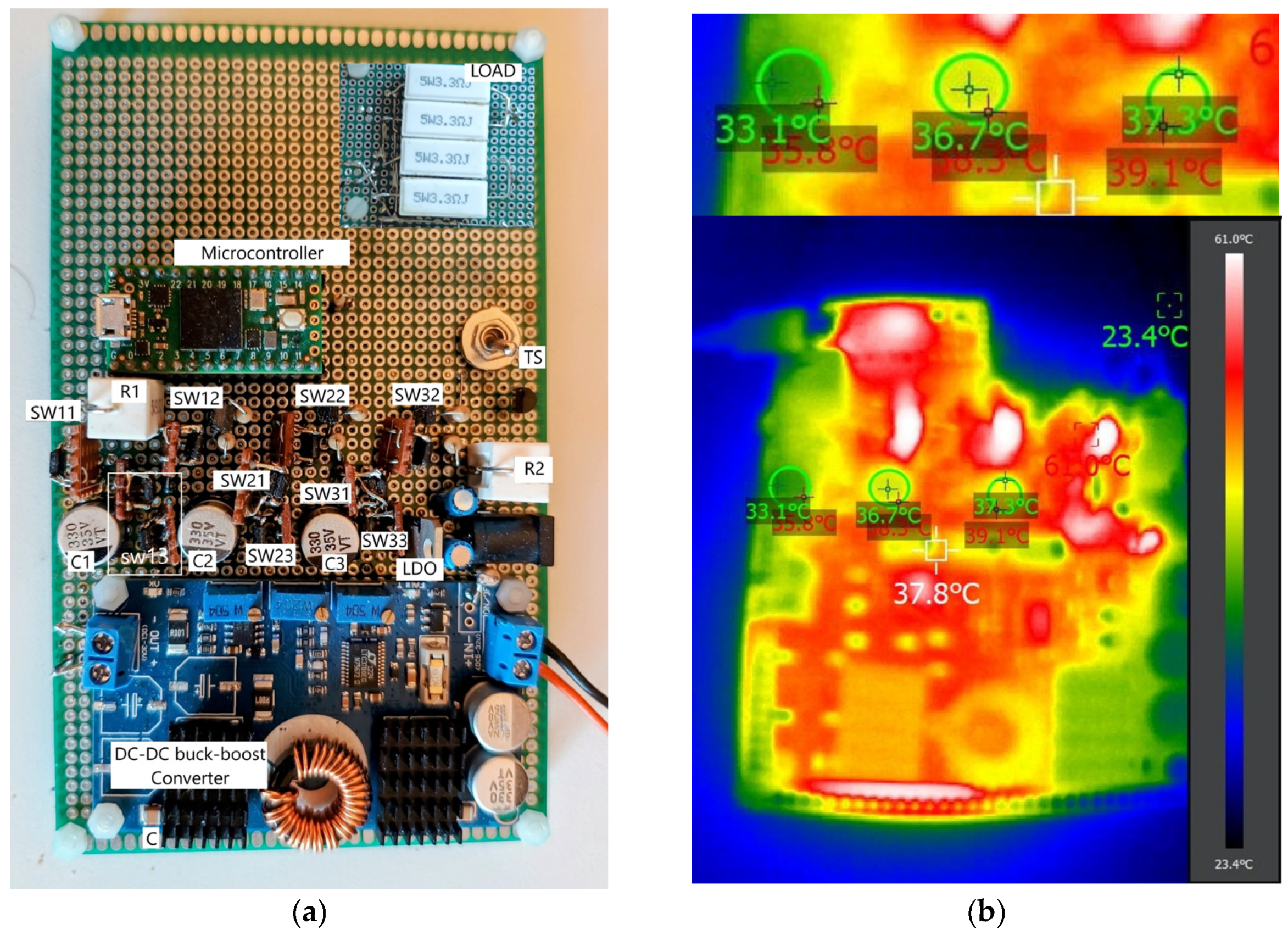
The experimental board corresponding to the diagram in Figure 5 is shown in Figure 8a. Figure 8b presents a thermal map of the board acquired with a thermal imager Hti-Xintai HT19. To determine the temperature variations in specific areas, the device’s IR ImageTools Software v1.0.0.13 was used.

3.2. Experimental Results

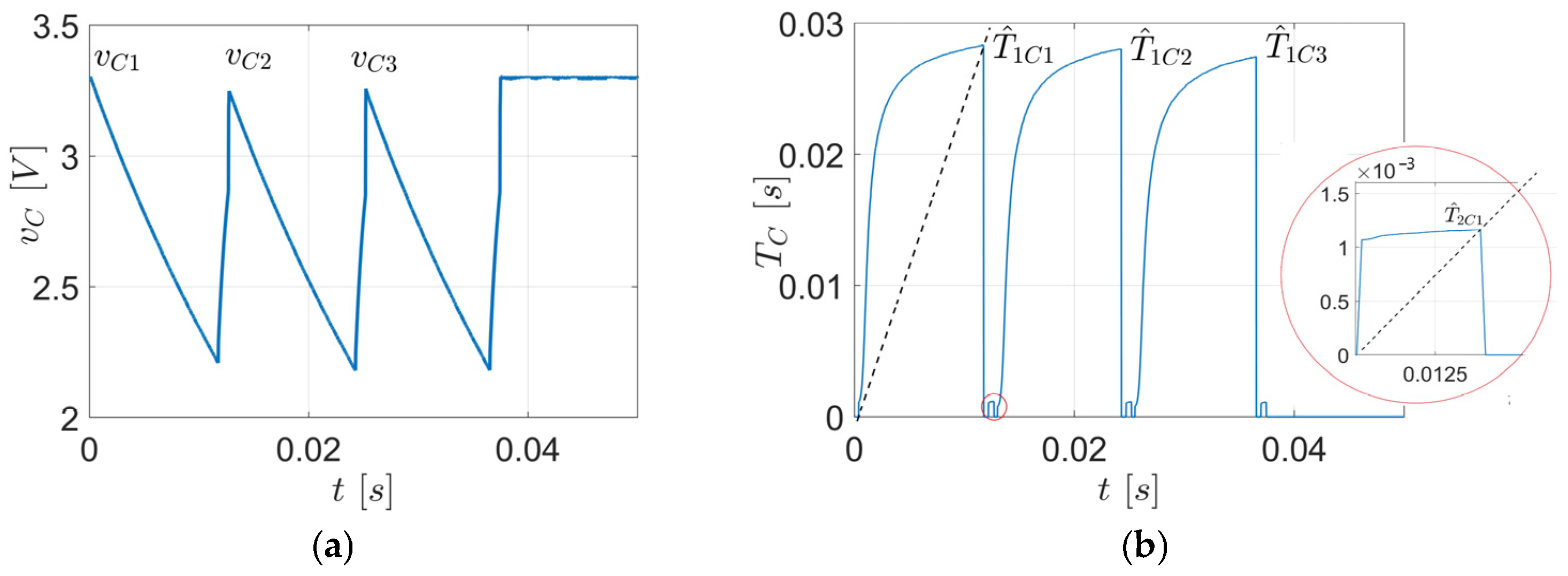
Figure 9a displays an estimation cycle consisting of the three estimation sequences of the capacitor parameters C1, C2, and C3. The cycle duration is  0.037341   s . The capacitors are monitored by voltage  v C  in the sequence C1-C2-C3. The beginnings of the sequences are noted as  v C 1 v C 2  and  v C 3 . Figure 9b details the results provided by PO2 during the cycle. The values of the time constants are obtained when condition (5) is met. Graphically, this moment corresponds to the abscissa of the intersection point between the half-line with slope 2.5, represented by the dashed line, and the curve  T ^ j C i t ,   i = 1 , 3 ¯ ,   j = 1 , 2 ¯  calculated by PO2. It is observed that the extension of the curves calculated for the charging processes,  T ^ 2 C i t ,   i = 1 , 3 ¯ , is much smaller than those corresponding to the discharging processes  T ^ 1 C i t ,   i = 1 , 3 ¯ .
Table 3 includes the following parameters for each discharge/charge sequence in Figure 9a: duration tn1, average duration of the discharge process  t d c h = t 1 ( t 0 + t n 1 ) , duration tn2, average duration of the charge process  t c h = t 2 ( t 1 + t n 2 ) , average intervals of voltage variation  v C  during the discharge/charge processes  v C d c h = v C ( t 0 + t n 1 ) , v C ( t 1 ) , respectively,  v C c h = v C ( t 1 + t n 2 ) , v C ( t 2 ) . The notations are those in Figure 4a. The values  t n 1  and  t n 2  were experimentally determined based on the characteristics of  T ^ 1 k k N  and  T ^ 2 k k N , so that PO2 does not monitor the transient regimes due to the switching in Figure 4b. The time interval ∆ between two consecutive sequences was zero.
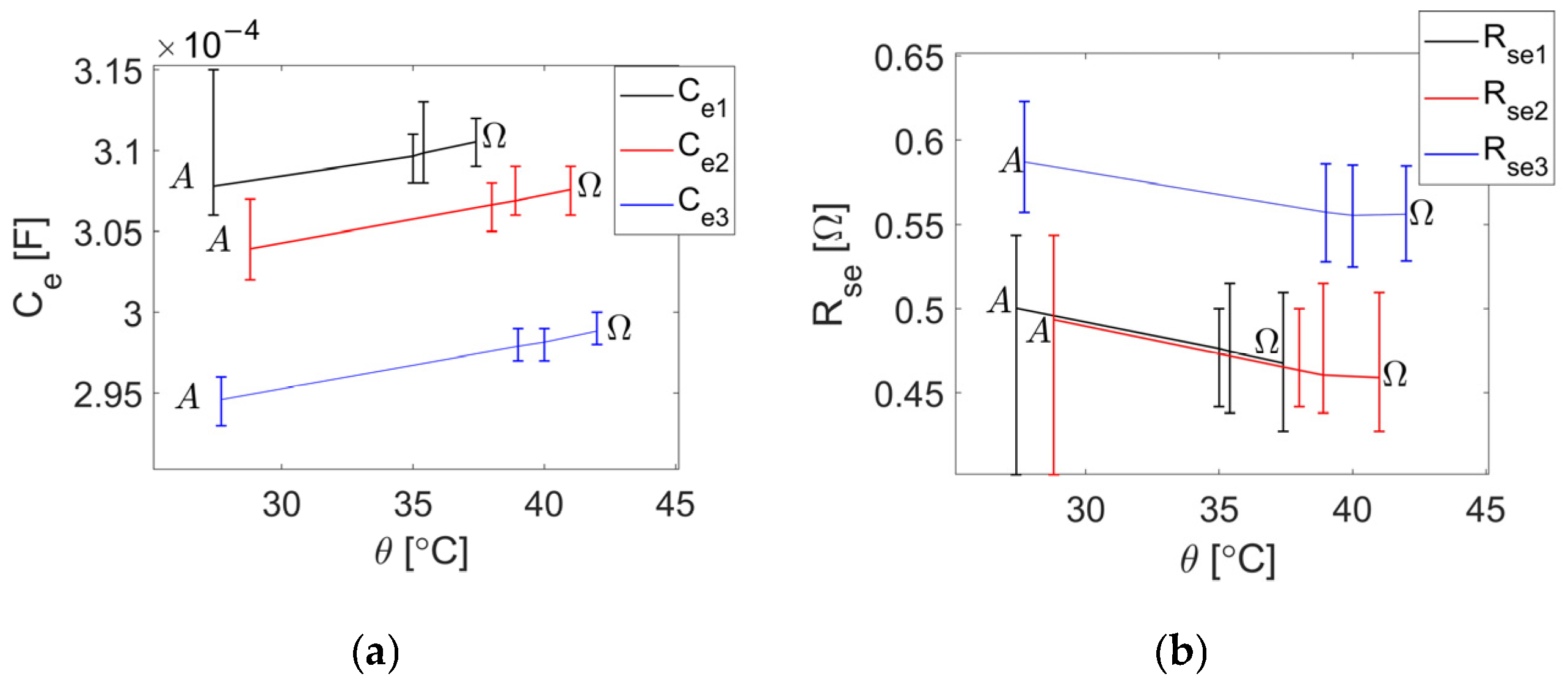
The thermal regime of the converter board varies during operation. After powering up the converter, the temperatures of different locations on the board increase and stabilize at values that depend on the board geometry, the operating regime, and the ambient temperature. Consequently, as Figure 8b suggests, the thermal distribution on the surface of the board and the components is non-uniform. The temperature status of the output filter capacitors is detailed in the inset at the top of the figure. It is observed that the temperatures differ both from one capacitor to another and on the surfaces of the capacitor capsules, depending on the measurement point:  33.1   ° C  and  35.8   ° C  for C1,  36.7   ° C  and  38.3   ° C  for C2,  a n d   37.3   ° C  and  39.1   ° C  for C3. In these circumstances, the values of the equivalent parameters of the capacitors were determined during 20 series of 400 cycles with intervals of approximately 12 min between two series. Table 4 summarizes the beginning and end of the experiment: series (A) and series (Ω). Figure 10 refers to four series: series (A), two intermediate series, and series ( Ω ). The vertical segments correspond to the ranges of the series values, and the connecting lines join the average values calculated for each series. The abscissas of the segments correspond to the temperatures of the capsule upper surface centers. The temperature characteristics  θ C 1 ( t ) θ C 2 ( t ) , and  θ C 3 ( t )  are strictly increasing, without suggesting an exponential variation. The series values of the ( Ω ) practically characterize the last five series of measurements.
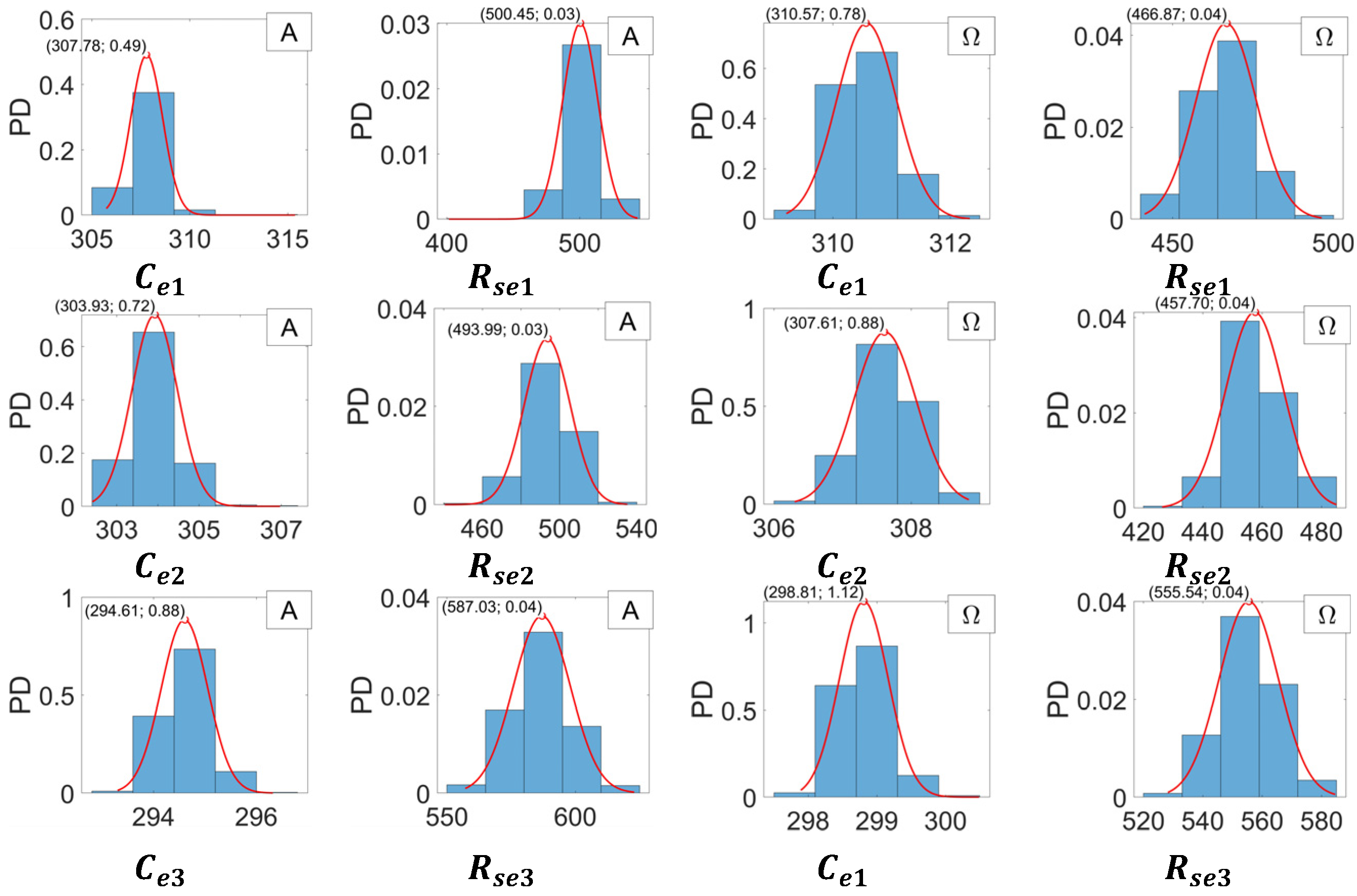
Figure 11 displays the probability distributions corresponding to the estimates made in the series (A) and ( Ω ).
During the estimation of the equivalent parameters of each capacitor in the bank, the capacitor is electrically isolated both from the converter and the load. As a result, the variation in the input voltage and the load value do not change the results mentioned in the article. When the input voltage, the load, and the configuration of the capacitor bank vary, the ripple changes occur. The influence of the change in the capacitance value on the ripple was highlighted in [29] (Figure 14c). Figure 12 illustrates these influences obtained experimentally for three input voltage values,  V i n =   8   V ,   9   V ,   10   V , and three values of  R L o a d   =   6.6   Ω ,   4.95   Ω ,   3.3   Ω . Zones 1, 2, 3, and 4 correspond to the operation of the converter with C1 not connected, C2 not connected, C3 not connected, with all capacitors connected. During the measurement process, the average value of the  V L o a d  voltage decreases by about  2.5   m V . It is also observed that independently of the estimation process: (i) when the load current increases (decrease of  R L o a d ) the average voltage on the load decreases by about  2   m V ; (ii) disconnecting a capacitor has a similar effect to increasing the load; and (iii) the influence of disconnecting a capacitor is related to its capacitance. These last three findings characterize the converter.

4. Discussion

(i)
The experiments performed with the DC–DC converter in Figure 5 confirm the applicability of the principle diagram in Figure 3. Moreover, the principle of estimating the parameters of the output filter capacitors can be applied for banks with more than three capacitors. In this case, scalability issues may arise, for example, regarding the number and compatibility of the microcontroller input/outputs needed for connecting the VEN.
(ii)
The sum of the times in Table 3 indicates that a cycle of estimating the parameters of the three-capacitor bank is performed online and in real time, in less than  37   m s .
(iii)
Within each series of estimates, the temperatures of the three capacitors were different. During the experiments, they increased with effect on the average values of the equivalent parameters (Table 4) by increasing  C e  and decreasing  R s e .
  • Considering that the stabilized equivalent mean values (line 1 of the series (Ω)) are correct, it is found that the values of  C e 1 C e 2  and  C e 3  of the series (A) are lower by approximately 1%, and the values of  R s e 1 R s e 2  and  R s e 3  are higher by approx. 6–7% (last line of Table 4). Apart from  C e 3 , for any segment in Figure 10, the ranges of the estimated values intersect, although the mean values of  C e / R s e  monotonically increase/decrease.
  • The probability distributions in Figure 11, correlated with the data in Table 4, allow us to consider that the accuracy of the estimates is very good: below  1   μ F  in the case of equivalent capacitances and about  11   m Ω  in the case of ESR.
  • The purpose of the configuration illustrated in Figure 3 is to estimate the capacitor parameters during the converter’s current operation. The triggering estimation depends on the management of diagnosis and prognosis. The above observations are crucial for defining these moments. The decision can only be made by the designer and/or converter user. They should also take into consideration the specific constructive elements, the environmental conditions, and the working regime of the converter.
(iv)
In the discharge/charge circuits of a capacitor, both the equivalent resistance of the capacitor and the conduction resistance  r D S o n  of the switch transistor act as resistive elements. Therefore, the  R s e  values in Table 4 correspond to the sum  R s e = R s e + r D S o n , where  R s e  is the corrected value of ESR. The MOSFET transistors were chosen with a minimum control signal in the grid and conduction resistance  r D S o n  as low as possible, i.e.,  r D S o n = 10   m . Their effect on the ESR values in the  Ω  series of Table 4 is illustrated in Table 5. The  R s e  values are reduced by 2.14% for C1, 2.18% for C2 and 1.8% for C3. The mean square deviation in percentage remains practically the same. If the bank capacitors had been of better quality, with a lower ESR, the  r D S o n  weight in the estimation result using the presented method would have been higher.
(v)
A notable fact is the closeness of the frequencies associated with the average values of the equivalent parameters in Table 4 established on the frequency characteristics in Figure 7. They are given in Table 6 for the series of experiments ( Ω ). The fact that the pairs of values ( C e i R s e i ),  i = 1 , 3 ¯  correspond, according to Figure 7, to very close average frequencies ( 58.27   H z 56.785   H z 54.63   H z ), suggests that the presented estimation method associates an equivalent frequency  f e  to the equivalent values of the capacitor parameters. The attribute “equivalent” designates in this case both the association with the equivalent circuit and the association with the capacitor discharge/charge voltage signal spectrum.
(vi)
PO2 can be implemented on the same microcontroller interfaced with the converter integrated circuit, and the diagram in Figure 5 can be partially integrated into a single dedicated circuit [31]. The estimation cycle can be triggered whenever it is relevant during the operation of the converter, and the calculated parameters can be transmitted to the upper level of a maintenance application. It is also important to note that the number of monitored capacitors can be adapted as needed.
(vii)
The experiments were performed with a DC–DC buck-boost converter made with the LTC 3780 integrated circuit operating in buck mode at an output voltage of  3.3   V  and with a resistive load  R L o a d = 6.6   Ω  aimed to validate the method for estimating the parameters of a filter capacitor bank. These values were chosen, on the one hand, from conditions of direct compatibility with the input voltage levels of the microcontroller, and on the other hand, so as not to charge the converter with a large load. To apply the proposed method for higher output voltage levels, both in buck and boost mode, it is necessary to complete the configuration with level shifter stages for adapting the converter voltages to the microcontroller.
(viii)
The estimation of capacitor parameters with the proposed model should be considered as an operation, part of the maintenance strategy chosen by the converter user. For this purpose, the microcontroller transmits to a higher level of maintenance structure the estimated values of C and ESR. The following aspects are useful for adopting a strategy:
  • PO2 estimates the capacitance and ESR values by repeating cycles that may contain 1, 2, or 3 sequences.
  • The estimations can be made continuously on preset time intervals, without interrupting the converter operation. They can highlight the following, in real time: (i) the aging effect when the capacitance decreases and the ESR increases, and (ii) the large variations in the time constants specific to the pre-breakdown regime when the insulation resistance decreases.
  • Through additional operations, after each estimation cycle consisting of three sequences, an equivalent bank capacity can be calculated based on a bank model.
  • The schematic allows, through additional control, performing maintenance operations at the capacitor level, not the capacitor bank. Thus, extracting and replacing a faulty capacitor can be discharged and disconnected without converter shutdown, as in the case of the estimation. This means a higher level of reliability at the system level by avoiding the system shutdown.

5. Conclusions

The article presents a method for determining the equivalent parameters of the capacitors that make up the capacitor bank of the output filter of a DC–DC buck converter. The method provides a usable tool for monitoring the condition of the capacitors. The estimated parameters correspond to the equivalent series R–C circuit of a capacitor. The capacitors of the bank are connected in parallel. The estimation is performed online and in real time using a parameter observer, without interrupting the converter operation. The observer successively processes the signals at the capacitor terminals during a discharge/charge sequence. The absence of auxiliary sensors represents a notable advantage of the method. The experiments using a converter, with  3.3   V  output voltage and a filtering bank consisting of  3   ×   330   μ F / 35   V  aluminum capacitors proved a good precision and a duration for the 6-parameter estimation cycle of approximately  38   m s .
The application of the method in circuits that use capacitor banks, primarily for filtering, involves solving practical problems such as the following: creating the possibility of isolating the capacitors from the circuit during parameter estimation, adapting VEN to the circuit voltages, interfacing with the microcontroller, and calibrating PO2 depending on the dynamics of the discharge/charge processes. All these problems, together with the proposed method, must also be analyzed from the point of view of the reliability and maintenance cost of the more complex structure that results from the implementation of the method.
The main direction for future research is to adapt the method to DC–DC boost–buck converters.

Author Contributions

Conceptualization, T.-L.D., C.B., D.-V.C. and S.N.; methodology, C.B., D.-V.C. and T.-L.D.; software, D.-V.C. and C.B.; validation, T.-L.D., C.B., D.-V.C. and S.N.; formal analysis, T.-L.D.; investigation, C.B. and D.-V.C.; resources, S.N., C.B. and D.-V.C.; data curation, C.B. and D.-V.C.; writing—original draft preparation, T.-L.D.; writing—review and editing, T.-L.D., C.B., D.-V.C. and S.N.; visualization, C.B. and D.-V.C.; supervision, T.-L.D. All authors have read and agreed to the published version of the manuscript.

Funding

This research received no external funding.

Data Availability Statement

The original contributions presented in this study are included in the article. Further inquiries can be directed to the corresponding author.

Conflicts of Interest

The authors declare no conflicts of interest.

Abbreviations

The following abbreviations are used in this manuscript:
ESREquivalent Serial Resistance
LDOLow Dropout Regulators
POParameter Observer
PO2Parameter Observer on Two Edges
RULRemaining useful life
VENVariable Electrical Network

Appendix A

Table A1. Papers related to capacitor bank.
Paper/Year of PublicationTreated IssueComplexity/Prototype/SimulationCapacitors MonitoringObservations
[17]/2014Methods for increasing the reliability of capacitors for DC-link applications in power electronic convertersOverview paper-- Capacitor banks are treated as a whole
- A method for designing capacitor banks to optimize reliability, cost, and size
[18]/2016Description and classification of methods for monitoring the health of capacitors Overview paper-Data and advanced algorithm-based methods category treats power electronic converters as a black box or semi-black box (can be used for capacitor banks)
[14]/2018Health monitoring of each capacitor of a bank using Physics of Failure models updated sequentially with Extended Kalman Filter algorithm- Prototype with experimental results after 400 h of aging
- DSP used for acquisition and data processing
- No individual sensor for each capacitor needed
Estimates capacity and ESR for each capacitor of a bank based on models and electrical inputs measured with sensors for the entire bank-
[19]/2019DC-link capacitors in three-phase pulsewidth modulation ac–dc–ac power convertersA VEN unit is used for each capacitor in the bank.C and ESR of dc-link capacitors are estimated through VEN units during the discharging process.A series capacitor bank consisting of several capacitors is employed to sustain the intermediate circuit voltage.
[12]/2020Health monitoring techniques for capacitors used in power electronics converters- Overview paper
- The monitoring methods mentioned vary in their level of complexity
- Methods for monitoring the parameters of individual capacitors;
- Monitoring the equivalent parameters of the capacitor bank as a whole
Considerations about mixed banks containing multiple types of capacitors.
[20]/2022Design of a Rogowski coil for online monitoring of a single-capacitor in the dc bank.Complex as Rogowski coils sensor are integrated in PCB and offer small signals.- Monitoring each capacitor in DC-link bank
- Practical performance assessment of the circuit
ESR at high-frequency region as a new aging indicator.
[21]/2022Quasi off-line monitoring of the time constant for discharging circuit during converter shutdown - PrototypeMonitoring for DC-link bank capacitorsOptimizing the sampling frequency to reduce noises
[22]/2023Monitor ESR and C of each capacitor in a dc-link capacitor bank with PCB integrated Rogowski coils as sensors.Complex as Rogowski coils and other sensors are integrated in the PCB circuit. - Monitoring individual capacitor in the bank;
- After temperature standardization provides monitoring and prediction for each capacitor
- Theoretical analysis, simulation and laboratory experimental setup using a single-phase inverter.
[23]/2023Monitor capacitor condition in a dc-link of power converters, following active methodology by signal injecting to estimate the ESR and C of a dc-link capacitor.Complex as it implies signal injectionMonitoring of capacitor DC-link bank as a whole- Capacitor parameter estimation method comparison from execution time point of view;
- Theoretical analysis and microgrid laboratory experimental setup
[24]/2025High-gain adaptive observer for estimating floating voltages and monitoring capacitors aging in multicell convertersSimulation for 3-cell converter- Simultaneous estimation of states and parameters in a p-cell converter,
- Does not apply to each capacitor of a bank
- Good balance between estimation accuracy and computational feasibility
- Needs a high-performance current sensor and sufficiently powerful computing software for commercial implementation

References

  1. Bacha, S.; Munteanu, I.; Bratcu, A.I. Power Electronic Converters Modeling and Control; Springer: London, UK, 2014. [Google Scholar] [CrossRef]
  2. Chen, Y.; Zhang, B. Equivalent-Small-Parameter Analysis of DC/DC Switched-Mode Converter; CPSS Power Electronics Series; Springer: Singapore, 2019. [Google Scholar] [CrossRef]
  3. Bhargava, C.; Sharma, P.K.; Senthilkumar, M.; Padmanaban, S.; Ramachandaramurthy, V.K.; Leonowicz, Z.; Blaabjerg, F.; Mitolo, M. Review of Health Prognostics and Condition Monitoring of Electronic Components. IEEE Access 2020, 8, 75163–75183. [Google Scholar] [CrossRef]
  4. Amaral, A.M.R.; Cardoso, A.J.M. Estimating Aluminum Electrolytic Capacitors Condition Using a Low Frequency Transformer Together with a DC Power Supply. In IEEE International Symposium on Industrial Electronics; Institute of Electrical and Electronics Engineers: New York, NY, USA, 2010; pp. 815–820. [Google Scholar] [CrossRef]
  5. Leong, C.; Wong, C.; Lan, C. An Online ESR Estimation Method for Output Capacitor of DC-DC Boost Converter Without Current Sensor. IEEE Trans. Power Electron. 2024, 40, 2196–2209. [Google Scholar] [CrossRef]
  6. Buiatti, G.M.; Amaral, A.M.R.; Cardoso, A.J.M. An Online Technique for Estimating the Parameters of Passive Components in Non-Isolated DC/DC Converters. In Proceedings of the IEEE International Symposium on Industrial Electronics, Vigo, Spain, 4–7 June 2007; pp. 606–610. [Google Scholar] [CrossRef]
  7. Cen, Z. Capacitance Online Estimation Based on Adaptive Model Observer. MATEC Web Conf. 2016, 77, 02006. [Google Scholar] [CrossRef]
  8. TDK. B32672L Film Capacitors Metallized Polypropylene Film Capacitors (MKP); TDK: Tokyo, Japan, 2019. [Google Scholar]
  9. Li, H.; Huang, X.; Li, Z.; Li, H.; Wang, W.; Wang, B.; Zhang, Q.; Lin, F. Modeling of ESR in Metallized Film Capacitors and Its Implication on Pulse Handling Capability. Microelectron. Reliab. 2015, 55, 1046–1053. [Google Scholar] [CrossRef]
  10. Zhao, Z.; Davari, P.; Lu, W.; Wang, H.; Blaabjerg, F. An Overview of Condition Monitoring Techniques for Capacitors in DC-Link Applications. IEEE Trans. Power Electron. 2021, 36, 3692–3716. [Google Scholar] [CrossRef]
  11. Amaral, A.M.R.; Laadjal, K.; Cardoso, A.J.M. Assessment of Aluminum Electrolytic Capacitors Health Status Through Signal-Based Techniques. In Proceedings of the 2024 IEEE 21st International Power Electronics and Motion Control Conference, PEMC, Pilsen, Czech Republic, 30 September–3 October 2024; Institute of Electrical and Electronics Engineers Inc.: New York, NY, USA, 2024. [Google Scholar] [CrossRef]
  12. Dang, H.L.; Kwak, S. Review of Health Monitoring Techniques for Capacitors Used in Power Electronics Converters. Sensors 2020, 20, 3740. [Google Scholar] [CrossRef] [PubMed]
  13. Sundararajan, P.; Sathik, M.H.M.; Sasongko, F.; Tan, C.S.; Pou, J.; Blaabjerg, F.; Gupta, A.K. Condition Monitoring of DC-Link Capacitors Using Goertzel Algorithm for Failure Precursor Parameter and Temperature Estimation. IEEE Trans. Power Electron. 2020, 35, 6386–6396. [Google Scholar] [CrossRef]
  14. Gupta, Y.; Ahmad, M.W.; Narale, S.; Anand, S. Health Estimation of Individual Capacitors in a Bank with Reduced Sensor Requirements. IEEE Trans. Ind. Electron. 2019, 66, 7250–7259. [Google Scholar] [CrossRef]
  15. Chen, M.; Wang, H.; Wang, H.; Blaabjerg, F.; Wang, X.; Pan, D. Reliability Assessment of Hybrid Capacitor Bank Using Electrolytic- and Film-Capacitors in Three-Level Neutral-Point-Clamped Inverters. In Proceedings of the IEEE Applied Power Electronics Conference and Exposition, Anaheim, CA, USA, 17–21 March 2019; pp. 2826–2832. [Google Scholar] [CrossRef]
  16. Narale, S.B.; Kumar, P.N.; Ahmad, M.W.; Verma, A.; Anand, S. Reliability Comparison of Dc Link Capacitor Bank for Different Configurations. In Proceedings of the IEEE International Conference on Industrial Technology, Melbourne, Australia, 13–15 February 2019; pp. 1023–1027. [Google Scholar] [CrossRef]
  17. Wang, H.; Blaabjerg, F. Reliability of Capacitors for DC-Link Applications in Power Electronic Converters—An Overview. IEEE Trans. Ind. Appl. 2014, 50, 3569–3578. [Google Scholar] [CrossRef]
  18. Soliman, H.; Wang, H.; Blaabjerg, F. A Review of the Condition Monitoring of Capacitors in Power Electronic Converters. IEEE Trans. Ind. Appl. 2016, 52, 4976–4989. [Google Scholar] [CrossRef]
  19. Wu, Y.; Du, X. A VEN Condition Monitoring Method of DC-Link Capacitors for Power Converters. IEEE Trans. Ind. Electron. 2019, 66, 1296–1306. [Google Scholar] [CrossRef]
  20. Liu, Y.; Bai, J.; Huang, M.; Zha, X. An Online Monitoring Method for Single Aluminum Electrolytic Capacitor in the DC Bank of Single-Phase Inverter Based on the Rogowski Coil. IEEE Trans. Power Electron. 2022, 37, 12647–12658. [Google Scholar] [CrossRef]
  21. Baumann, T.F.; Papastergiou, K.; Garcia, R.M.; Peftitsis, D. A Quasi-Offline Condition Monitoring Method of DC-Link Capacitor Banks in Accelerator Power Converters. In Proceedings of the 24th European Conference on Power Electronics and Applications (EPE’22 ECCE Europe), Hanover, Germany, 5–9 September 2022; pp. 1–12. [Google Scholar]
  22. Zhu, M.; Liu, Y.; Huang, M.; Li, Z.; Zha, X. A Digital Twin System of Capacitive DC Bank Using Rogowski Coil to Monitor Individual Capacitors. IEEE Trans. Power Electron. 2023, 38, 9251–9260. [Google Scholar] [CrossRef]
  23. Ribeiro, R.L.A.; Sangwongwanich, A.; Alves, D.K.; Blaabjerg, F.; de Oliveira Alves Rocha, T.A. Wavelet-Based Estimation Method for Online Condition Monitoring of Dc-Link Capacitors of Distributed Energy Resources. Int. J. Electr. Power Energy Syst. 2023, 151, 109141. [Google Scholar] [CrossRef]
  24. Nait Slimani, B.; Ghanes, M.; Djennoune, S. High-Gain Adaptive Observer for Floating Voltages Estimation and Capacitor Aging Monitoring in Multicell Converters. Eng. Sci. Technol. Int. J. 2025, 65, 102036. [Google Scholar] [CrossRef]
  25. Cen, Z.; Stewart, P. Condition Parameter Estimation for Photovoltaic Buck Converters Based on Adaptive Model Observers. IEEE Trans. Reliab. 2017, 66, 148–160. [Google Scholar] [CrossRef]
  26. Meng, J.; Chen, E.X.; Ge, S.J. Online E-Cap Condition Monitoring Method Based on State Observer. In Proceedings of the 2018 IEEE International Power Electronics and Application Conference and Exposition, PEAC, Shenzhen, China, 4–7 November 2018. [Google Scholar] [CrossRef]
  27. Gara, H.; Ben Saad, K. Fault Detection for Linear Switched Systems Based on a Bank of Luenberger Observers. In Proceedings of the 2018 International Conference on Advanced Systems and Electric Technologies, IC_ASET, Hammamet, Tunisia, 22–25 March 2018; Institute of Electrical and Electronics Engineers Inc.: New York, NY, USA, 2018; pp. 92–97. [Google Scholar] [CrossRef]
  28. Bărbulescu, C.; Căiman, D.V.; Nanu, S.; Dragomir, T.L. Implementation of Parameter Observer for Capacitors. Sensors 2023, 23, 948. [Google Scholar] [CrossRef] [PubMed]
  29. Căiman, D.V.; Bărbulescu, C.; Nanu, S.; Dragomir, T.L. DC-DC Buck Converters with Quasi-Online Estimation of Filter Capacitor Equivalent Parameters. Appl. Sci. 2024, 14, 10756. [Google Scholar] [CrossRef]
  30. LTC3780 Datasheet and Product Info|Analog Devices. Available online: https://www.analog.com/en/products/ltc3780.html (accessed on 21 July 2025).
  31. PJRC. Teensy 4.0. Available online: https://www.pjrc.com/store/teensy40.html (accessed on 4 August 2025).
Figure 1. Elementary circuits explaining: (a) discharging a capacitor across different resistors; and (b) charging and discharging a capacitor using different resistors.
Electronics 14 03614 g001
Figure 2. (a) Connection of PO2 to the observed MS process; and (b) signal applied to PO2 input during a capacitor discharge/charge sequence.
Electronics 14 03614 g002
Figure 3. Schematic diagram for estimating the parameters of a bank of three capacitors.
Electronics 14 03614 g003
Figure 4. A discharge/charge sequence: (a) variation in the measured voltage  v C ( t )  during a sequence; and (b) switch states during a sequence and switching commands.
Electronics 14 03614 g004
Figure 5. Schematic diagram of a converter with output filtering bank and estimation of capacitor parameters with a PO2.
Electronics 14 03614 g005
Figure 6. Flowchart of estimating capacitors equivalent parameters.
Electronics 14 03614 g006
Figure 7. Frequency characteristics of C1, C2, and C3: (a) Capacitance C; (b) ESR Rs; and (c) Impedance Z.
Electronics 14 03614 g007
Figure 8. Experimental setup: (a) photograph; and (b) thermal map example (emissivity factor = 0.95). Temperature drops in an interval of  θ 23.4   ° C ,   61.0   ° C
Electronics 14 03614 g008
Figure 9. An estimation cycle for equivalent time constants: (a) signal processed by PO2; and (b) curves  T ^ j C i t , i = 1 , 3 ¯ , j = 1 , 2 ¯  used for computing the time constants  T ^ i 1 , T ^ i 2 , i = 1 , 3 ¯ .
Electronics 14 03614 g009
Figure 10. Ranges of the estimated parameters: (a) capacitances; and (b) ESR. Cases (A) and ( Ω ) correspond to lines 2 in Table 4.
Electronics 14 03614 g010
Figure 11. Probability distributions of the estimated values for the equivalent parameters of capacitors in the (A) and ( Ω ) series. The average values are those in Table 4, represented with more decimal places.
Electronics 14 03614 g011
Figure 12. Influence of  V i n  și  R L o a d  on converter output voltage: (a) the signal  V L o a d ( t )  for  R L o a d = 6.6   Ω  și  V i n = 8   V , 9   V , 10   V ; and (b) the signal  V L o a d ( t )  for  V i n = 9   V  and  R L o a d = 6.6   Ω , 4.95   Ω , 3.3   Ω .
Electronics 14 03614 g012
Table 1. Characteristics of some diagrams for estimating the equivalent parameters of filter capacitors in DC–DC buck converters.
IdFigure 7a, [29]Figure 7b, [29]Figure 7c, [29]Figure 7d, [29] Figure 3
1.11123
2.1122 or 42
3. C L o a d
&
C R V E N
C L o a d
&
C R V E N
C R 1 V E N
&
C R 2 V E N
C R 1 V E N
&
C R 2 V E N
C R 1 V E N
&
C R 2 V E N
4.PO2PO2POPOPO2
5.quasi-online
/quasi-online
quasi-online
/quasi-online
quasi-online
/online
1quasi-online+1online
/online
1quasi-online+2online
/online (*)
6.---successivesuccessive
7. 1 / 1 1 / 1 1 i n   2   s t a g e s
or
2 / 1
2 / 2 1 / 1  (**)
(*), (**) New features detailed below.
Table 2. Meaning of the Ids in Table 1.
Id.Meaning
1.Number of capacitors in the output filter.
2.Number of resistors in the VEN.
3.The process to which the capacitor is subjected during the estimation.
4.Type of parameter observer.
5.Participation of the monitored capacitors in the filtering operation during the estimation/continuity of the load connection to the converter during the estimation.
6.How to include the capacitors in the bank in the measurement process.
7.Number of discharges (↘)/charges (↗) supported by the evaluated capacitor during the estimation of the parameters.
Table 3. Numerical data corresponding to estimation cycle in Figure 9.
C1C2C3
t n 1 = 0.00024   s ,   t d c h = 0.01134   s ,   t n 2 = 0.0004   s ,
v C d c h  = [3.266088 V, 2.209389 V]
t n 1 = 0.00022   s ,   t d c h   =   0.01124   s ,   t n 2 = 0.00044   s ,
v C d c h  = [3.216883 V, 2.18035 V]
t n 1 = 0.00018   s ,   t d c h   =   0.011   s ,   t n 2 = 0.00054   s ,
v C d c h  = [3.216076 V, 2.181156 V]
t c h  = 0.00048 s,
v C c h  = [2.628035 V, 2.865994 V]
t c h  = 0.00046 s,
v C c h  = [2.606256 V, 2.845828 V]
t c h  = 0.000461 s,
v C c h  = [2.619162 V, 2.861154 V]
Table 4. The estimated equivalent parameters of PO2 resulting from the series A and from the series  Ω . (1—the average values of the 400 estimates,  C e i ¯ R s e i ¯ ; 2—the intervals in which the values in a series were located; 3—the mean square deviation in absolute values/percentage of the 400 estimates from the average value  σ · · ; 4—the number/percentage of the values in the series [ C e i ¯ σ · · , C e i ¯ + σ · · ] ,   [ R s e i ¯ σ · · ,   R s e i ¯ + σ · · ] . The last two lines of the table show the temperature variation and the deviation of the value in line (*) from the value in line (**), respectively.
C e 1 [F] R s e 1 [Ω] C e 2 [F] R s e 2 [Ω] C e 3 [F] R s e 3 [Ω]
(A)- θ C i θ C 1 = 27.4   ° C θ C 2 = 28.8   ° C θ C 3 = 27.7   ° C
1. (*)0.0003080.5003530.0003040.4935730.0002950.586933
2.[0.000306, 0.000315][0.401475, 0.543484][0.000302, 0.000307][0.440476, 0.535087][0.000293, 0.000296][0.55714, 0.622899]
3.8.13 × 10−7/
0.247%
0.01287/
2.572%
5.54 × 10⁻⁷/
0.169%
0.011034/
2.235%
4.51 × 10⁻⁷/
0.124%
0.010091/
1.719%
4.301/75.25%292/73%275/68.75%276/69%275/75.25%278/73%
(Ω)- θ C i θ C 1 = 37.4   ° C θ C 2 = 41   ° C θ C 3 = 42   ° C
1. (**)0.0003110.4676140.0003080.4589810.0002990.556098
2.[0.000309, 0.000312][0.42724, 0.509411][0.000306, 0.000309][0.4263, 0.513102][0.000298, 0.0003][0.528205, 0.584585]
3.5.18 × 10−7/
0.162%
0.00989/
2.114%
4.64 × 10⁻⁷/
0.148%
0.010116/
2.204%
3.67 × 10⁻⁷/
0.120%
0.009489/
1.706%
4.281/70.25%283/70.75%270/67.5%278/69.5%284/70.25%277/70.75%
Deviations of (*) from (**) θ C 1 = 10   ° C θ C 2 = 12.2   ° C θ C 1 = 14.3   ° C
−0.9646%+7%−1.2987%+7.5366%−1.3377%+5.5448%
Table 5. Corrected values of average values of ESR in line 1, series ( Ω ) of Table 4, taking into account the resistance  r D S o n  of the switch transistors.
R s e 1 [Ω] R s e 1 [Ω] R s e 2 [Ω] R s e 2 [Ω] R s e 3 [Ω] R s e 3 [Ω]
0.4676140.4576140.4589810.4489810.5560980.546098
Table 6. Frequencies extracted from the frequency characteristics of the capacitor bank corresponding to the average values of the equivalent parameters in line 1, series ( Ω ) of Table 4 and Table 5.
C e 1 [F] R s e 1 [Ω] C e 2 [F] R s e 2 [Ω] C e 3 [F] R s e 3 [Ω]
0.00031054 *0.4576140.0003075 *0.4489810.0002988374 *0.546098
53.88 Hz58.27 Hz55.3 Hz58.27 Hz52.49 Hz56.77 Hz
Electronics 14 03614 i001Electronics 14 03614 i001Electronics 14 03614 i001
f e 1 = 56.075   H z f e 2 = 56.785   H z f e 3 = 54.63   H z
(*) These capacitance values have not been rounded to correlate as accurately as possible with the frequency characteristics.
Disclaimer/Publisher’s Note: The statements, opinions and data contained in all publications are solely those of the individual author(s) and contributor(s) and not of MDPI and/or the editor(s). MDPI and/or the editor(s) disclaim responsibility for any injury to people or property resulting from any ideas, methods, instructions or products referred to in the content.