You are currently viewing a new version of our website. To view the old version click .
Electronics
  • Article
  • Open Access

5 September 2025

An E-Band High-Precision Active Phase Shifter Based on Inductive Compensation and Series Peaking Enhancement Techniques

,
,
,
and
1
School of Microelectronics, South China University of Technology, Guangzhou 511442, China
2
School of Artificial Intelligence, Zhuhai City Polytechnic, Zhuhai 519090, China
*
Author to whom correspondence should be addressed.
Co-first Authors.
This article belongs to the Collection Advanced Design Techniques and EDA Methodologies for Analog, RF and MM-Wave Circuit Design

Abstract

This paper presents the design and implementation of a 6-bit high-precision active vector-sum phase shifter (PS) operating in the E-band, fabricated using a 40 nm CMOS process. To generate high-quality in-phase and quadrature (I/Q) signals, a folded transformer-based quadrature generator circuit (QGC) employing inductive compensation is developed. Additionally, the series peaking enhancement technique is applied to improve overall gain and effectively extend the bandwidth. Measurement results demonstrate that the phase shifter achieves a 3 dB bandwidth from 72.3 GHz to 82.3 GHz. Within this range, the measured RMS phase error is merely 1.78–2.55 degrees without calibration, and the RMS gain error is 0.6–0.75 dB. The core area of the proposed phase shifter is 940 μm × 280 μm, and it consumes 57.2 mW of power with a 1.1 V supply.

1. Introduction

With the rapid advancement of industries such as automotive electronics, intelligent transportation, and industrial automation, coupled with the growing demand for high-speed, low-latency, and large-capacity wireless communication, millimeter-wave (mm-wave) wireless communication has emerged in recent years as a frontier in communication technology research. In particular, during the later stages of 5G evolution and in upcoming 6G systems, the mm-wave frequency band—with its abundant spectrum resources—has become widely recognized as a key enabler of ultra-high-data-rate transmission. Among these, high-speed wireless communication standards operating in the E-band (71–76 GHz and 81–86 GHz) have attracted significant attention, with related products and applications advancing rapidly. Within the family of mm-wave communication technologies, beamforming based on phased array systems has been extensively adopted across diverse scenarios due to its advantages in dynamic beam steering, enhanced signal quality, and interference suppression [1,2]. As the core component for implementing beamforming, the phase shifter (PS) plays a critical role, as its performance directly determines the beam accuracy and direction control capabilities of the system [3,4]. Currently, PSs are mainly divided into two categories: passive [5,6,7,8] and active types [9,10,11,12]. Passive structures include switch-type [13], reflective-type [14], and load–transmission-line types. Although these circuits feature relatively simple architectures, they generally suffer from drawbacks such as high insertion loss, large chip area, and limited control flexibility, which restrict their suitability for highly integrated systems. In contrast, active PSs offer clear advantages in terms of phase resolution, tuning speed, insertion loss, and integration density, making them particularly well-suited for mm-wave phased array systems that demand high frequency, high speed, and compact design. With the continued advancement of CMOS processes in the mm-wave frequency band, active PS implementations not only achieve better cost efficiency but also provide the technological foundation for large-scale system integration. Consequently, as a critical building block, the research and application of active PSs in modern mm-wave communication systems have become increasingly important, drawing growing attention from both academia and industry.
With the widespread use of phased array systems in high-frequency communication and radar applications, PS technology is encountering several new technical challenges: (1) PSs experience impedance fluctuations during phase state transitions, which can negatively impact the stability of the overall link gain. (2) Active PSs, due to their higher gain, can compensate for the losses in high-frequency millimeter waves, making them more commonly used in phased array systems than passive phase shifters. However, the quadrature generator circuit (QGC) of active PSs, when operating at high-frequency millimeter waves, is susceptible to parasitic effects that degrade both amplitude and phase performance at the output, ultimately affecting phase shifting accuracy. (3) Active PSs typically incorporate a digital-to-analog converter (DAC) array, which relies on numerous switching devices, potentially influencing both the overall link gain and bandwidth.
To address these challenges, several technical solutions have been proposed. For the issue of impedance fluctuations during PS phase switching, ref. [15] introduced a hybrid structure combining a 5-bit passive phase shifter with a 1-bit active PS. To enhance gain stability across different phase states, the passive PS employs a compensation technique with constant insertion loss, achieved by integrating an NMOS transistor into each module as an attenuator. This stabilizes insertion loss and ensures consistent link gain across phase states, though at the cost of increased area overhead due to the additional passive PS. To mitigate parasitic effects in the QGC, which degrade overall performance, ref. [16] proposed a self-calibration method that leverages on-chip calibration to improve PS accuracy. However, this approach increases both the phase-shifting response time and chip area. Finally, to address bandwidth limitations in the mm-wave frequency range, stagger-tuning technology is commonly employed in amplifiers, trading off some gain and area efficiency to achieve wider bandwidth.
Different from the mentioned designs, this paper proposes a complementary switch-type DAC array to address the impedance fluctuation issue during phase switching. Additionally, series peaking enhancement is employed to further improve the PS’s bandwidth and gain. To mitigate the impact of parasitic effects on the QGC, an inductance-compensated QGC based on a folded transformer structure is proposed, using inductance compensation to alleviate the deteriorating effects of parasitic elements. To verify the effectiveness of the overall concept and technology, this paper uses the TSMC 40 nm CMOS process for design and fabrication, and its validity is verified through testing. The structure of the paper is as follows: Section 2 presents the circuit design, including the compact impedance-compensated QGC and complementary switch-type I/Q path DAC. In addition, the series peaking enhancement technique and driver module are also analyzed in this section. Section 3 provides a comprehensive overview of the test results and performance analysis, including S-parameters, RMS gain error, and RMS phase error, as well as other key performance metrics that are critical to the evaluation of PS’s overall functionality and efficiency. Section 4 provides the conclusion, and also shows performance summary and comparisons to previous mm-wave PSs.

2. Circuit Design of the Proposed PS

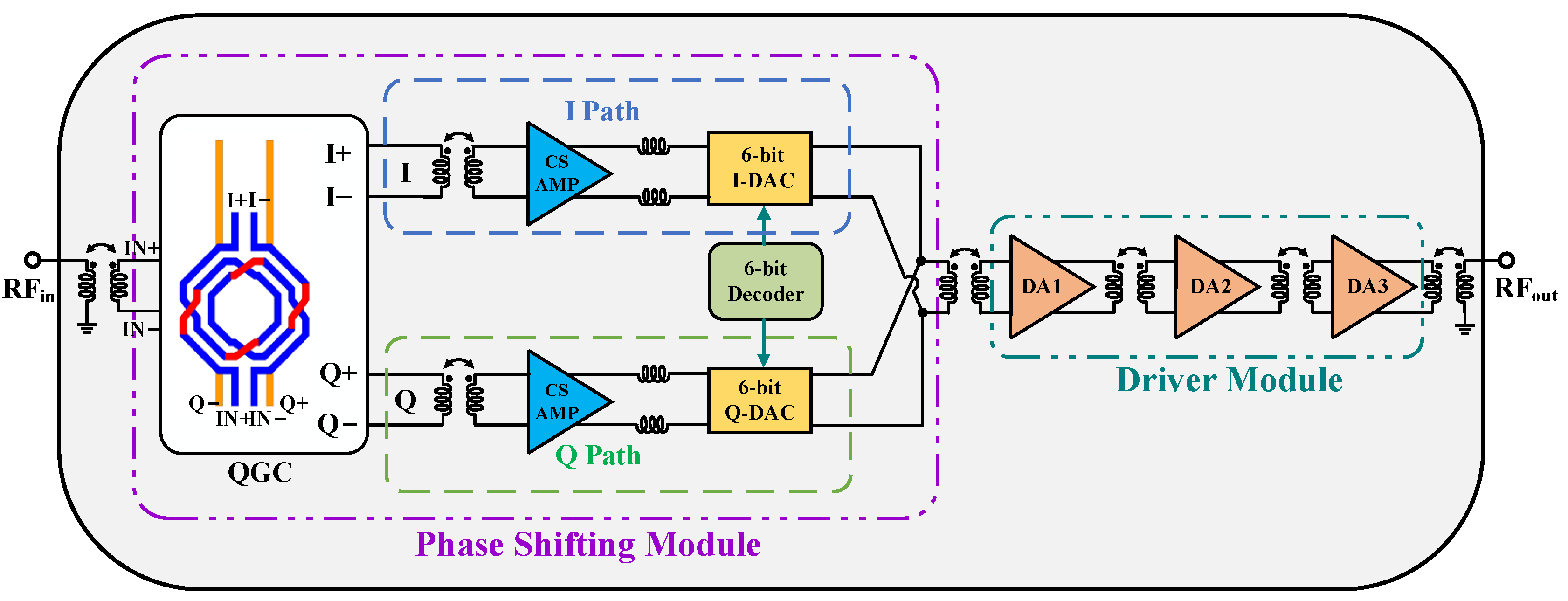
The schematic of the proposed PS is shown in Figure 1. The design integrates a compact impedance-compensated, capacitor-free QGC; a common-source (CS) amplifier; an I/Q DAC array with a 6-bit decoder for phase control; and a three-stage driver module. For measurement purposes, baluns are incorporated at both the input and output ports. The impedance-compensated, capacitor-free QGC is engineered to generate high-quality differential I/Q signals, while a transformer-based interstage matching network is employed between the QGC and the CS amplifier to maximize power transfer. The 6-bit I/Q DACs and decoder are co-designed to enable efficient vector summation, and series-peaking inductors are introduced between the CS amplifier and DACs to extend the overall bandwidth.
Figure 1. Schematic of the proposed PS.

2.1. Compact Impedance-Compensated and Capacitor-Free QGC

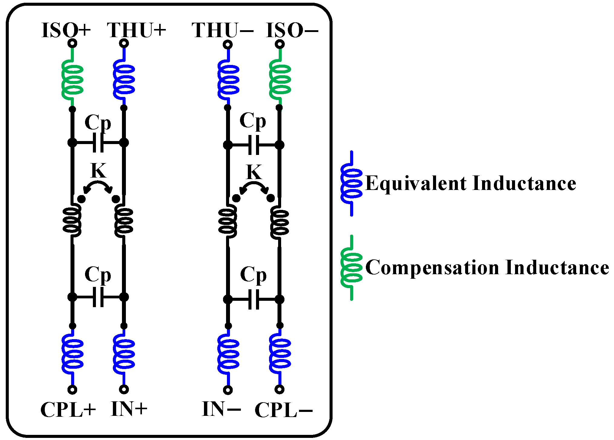
The QGC is employed to generate two equal-amplitude orthogonal signals. Building on the QGC described in [17], this section introduces an inductance-compensated QGC, which features four differential ports: input, coupling, through, and isolation ports. In the actual layout, three of the QGC ports (input, coupling, and through) are connected to external modules via metal traces, which effectively introduce inductance. To ensure optimal amplitude and phase performance, a compensating inductance is added at the isolation port, as depicted in Figure 2.
Figure 2. Schematic diagram of inductively compensated QGC.
The following analysis discusses the impact of the introduced equivalent inductance on the QGC. For an ideal QGC, its S-parameters can be expressed as (1)
S original = 0 0 j 2 1 2 0 0 1 2 j 2 j 2 1 2 0 0 1 2 j 2 0 0
where port 1 represents the input port, port 2 is the isolation port, port 3 is the through port, and port 4 is the coupling port.
From Soriginal, S41 = jS31 and S33 = S44, indicating that the matching conditions for the two output ports (through port and coupling port) are consistent, and the amplitude-phase performance is excellent.
The Z-matrix can be derived using (2) as
Z original = Z 0   ×   ( I +   S original )   ×   ( I S original ) 1
where Z0 = 50 Ω, and I is the 4th-order identity matrix.
When an equivalent inductance L is added to ports 1, 3, and 4, resulting in an equivalent series impedance of jωL, the new Z-matrix is
Z 1 = Z original + j ω L · diag ( 1 , 0 , 1 , 1 )
Next, the Z-matrix is converted into S-parameters, and the new four-port S-parameters are obtained as
S 1 = ( Z 1 Z 0 I )   ×   ( Z 1 +   Z 0 I ) 1 .
Assuming the added inductance is small, i.e., ωL ≪ Z0, then
S 1 = L ω L ω + 2 Z 0 j 2 L Z 0 ω σ 2 σ 6 2 σ 5 2 2 Z 0 2 σ 7 2 2 L Z 0 ω σ 7 2 L 3 ω 3 σ 1 j σ 6 3 σ 4 2 2 Z 0 ( σ 8 + 2 L Z 0 ω j + 2 Z 0 2 ) j σ 7 3 σ 5 σ 4 L ω ( σ 8 + σ 3 + 2 Z 0 2 ) j σ 7 3 2 L Z 0 2 ω σ 7 3 2 2 Z 0 2 σ 2 σ 6 2 2 2 Z 0 σ 1 ( L 2 ω 2 j + 2 L Z 0 ω 2 Z 0 2 j ) σ 6 3 2 L Z 0 2 ω σ 1 σ 6 3 L ω σ 1 ( σ 8 + σ 3 + 6 Z 0 2 ) j σ 6 3
where σ 1 = ( 2 Z 0 L ω j ) 3 , σ 2 = ( L ω + 2 Z 0 j ) 2 , σ 3 = 4 L Z 0 ω j , σ 4 = 4 2 Z 0 2 ( L ω + Z 0 j ) j σ 7 3 , σ 5 = 2 2 Z 0 2 j σ 7 2 , σ 6 = σ 8 + 4 Z 0 2 , σ 7 = 2 Z 0 + L ω j , σ 8 = L 2 ω 2 .
In S1, S41 = jS31 and S33 ≠ S44, indicating that the two output ports cannot simultaneously achieve matching while maintaining reliable amplitude-phase performance. After adding a compensation inductance L to port 2, the new four-port S-parameters, derived through the same process, are shown as
S 2 = σ 1 σ 2 σ 4 σ 3 σ 2 σ 1 σ 3 σ 4 σ 4 σ 3 σ 1 σ 2 σ 3 σ 4 σ 2 σ 1
where
  • σ 1 = L ω ( L 7 ω 7 + 2 L 6 Z 0 ω 6 j 10 L 5 Z 0 2 ω 5 12 L 4 Z 0 3 ω 4 j + 32 L 3 Z 0 4 ω 3 + 32 L 2 Z 0 5 ω 2 j + 16 L Z 0 6 ω + 32 Z 0 7 j ) σ 6   ,
  • σ 2 = 2 L Z 0 2 ω ( σ 5 + 2 L 4 Z 0 ω 4 + 4 L 3 Z 0 2 ω 3 j + 8 L 2 Z 0 3 ω 2 + 24 L Z 0 4 ω j 16 Z 0 5 ) σ 6 ,
  • σ 3 = 4 2 Z 0 3 ( σ 5 3 L 4 Z 0 ω 4 8 L 3 Z 0 2 ω 3 j + 4 L 2 Z 0 3 ω 2 8 L Z 0 4 ω j + 8 Z 0 5 ) σ 6 ,
  • σ 4 = 2 2 Z 0 2 ( L 6 ω 6 j + 2 L 5 Z 0 ω 5 + 6 L 4 Z 0 2 ω 4 j + 16 L Z 0 5 ω + 16 Z 0 6 j ) σ 6 ,
  • σ 5 = L 5 ω 5 j , σ 6 = L 8 ω 8 8 L 6 Z 0 2 ω 6 + 32 L 4 Z 0 4 ω 4 + 64 L 2 Z 0 6 ω 2 + 64 L Z 0 8 .
In S2, S41 = jS31 and S33 = S44, indicating that the two output ports can achieve matching while maintaining excellent amplitude-phase performance.
The above analysis uses an ideal model to illustrate the improvement effect of adding compensation inductance to the QGC. In practical circuit layouts, the equivalent inductance introduced by metal traces at the three ports is not identical, and there is usually the influence of parasitic capacitance. Therefore, the S-parameters will become more complex. To verify the effectiveness of the proposed QGC with compensation inductance, a circuit simulation is performed. The QGCs with and without inductive compensation structures are placed in the phase shifting module for simulation, and their respective RMS phase errors are calculated. The results are shown in Figure 3. The simulation results indicate that after adding inductance at the isolation port of the QGC, the RMS phase error of the PS is improved. At a frequency of 77 GHz, the RMS phase error without inductance is 2 degrees, while with the added inductance, it improves to 1.6 degrees, which is a 20% performance enhancement. The compensation inductor is 41.5 pH at 77 GHz in this design.
Figure 3. RMS phase error of phase shifting module with and without compensation inductance.

2.2. Complementary Switch-Type I/Q Path DAC Design

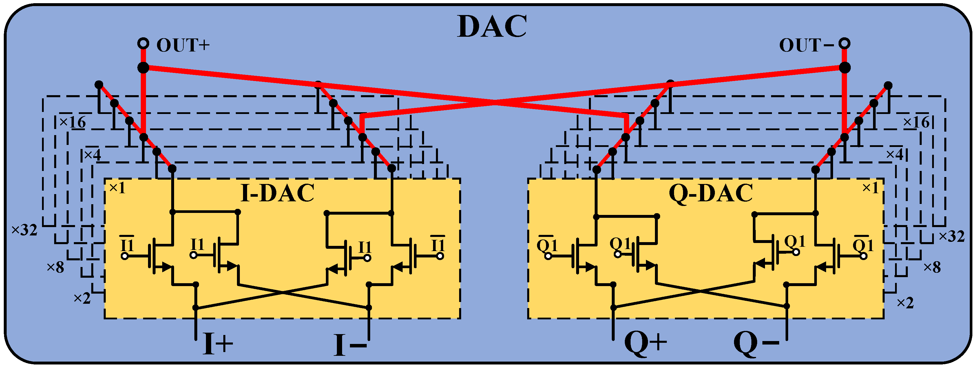
The circuit schematic of the I/Q dual DAC array is shown in Figure 4. I+/I− and Q+/Q− are the differential input ports, and OUT+/OUT− are the differential output ports. The transistors in the DAC are controlled by a 6-bit decoder for their on and off states. To achieve high-precision phase synthesis, the width ratio of the transistors in the same group is set to 1:2:4:8:16:32. The minimum transistor size is 850 nm.
Figure 4. Schematic of complementary switch-type I/Q Path DAC.
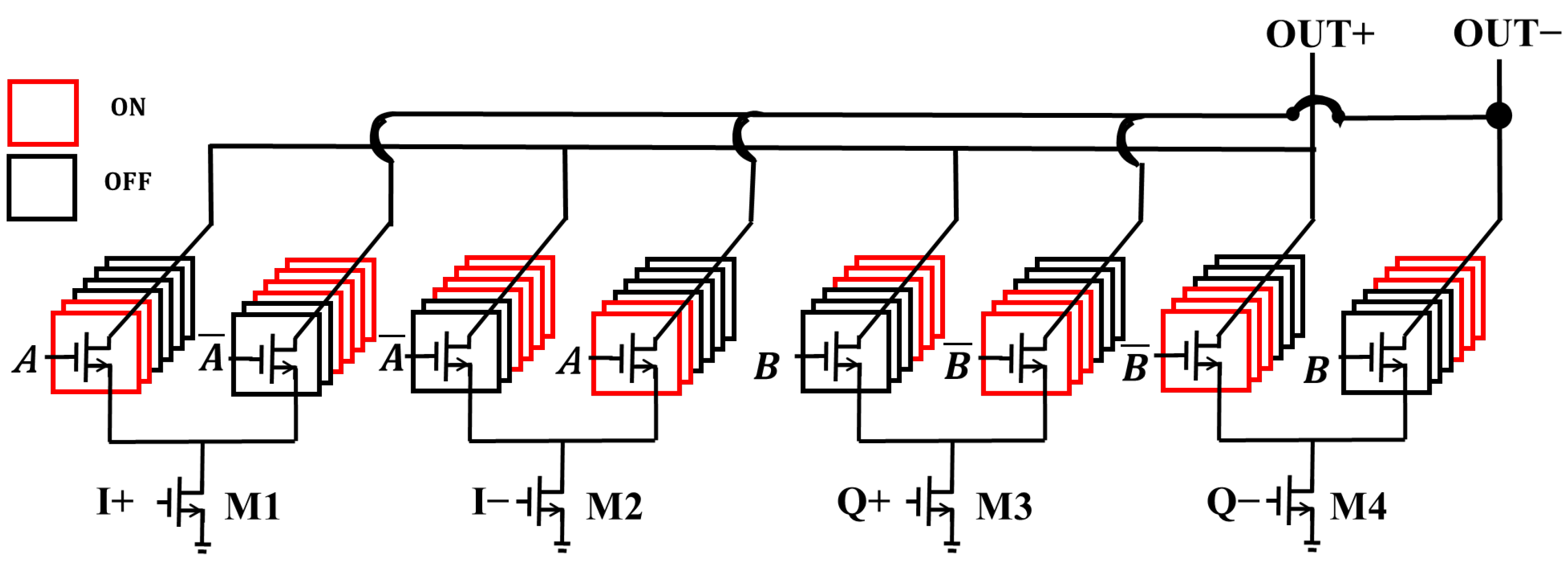
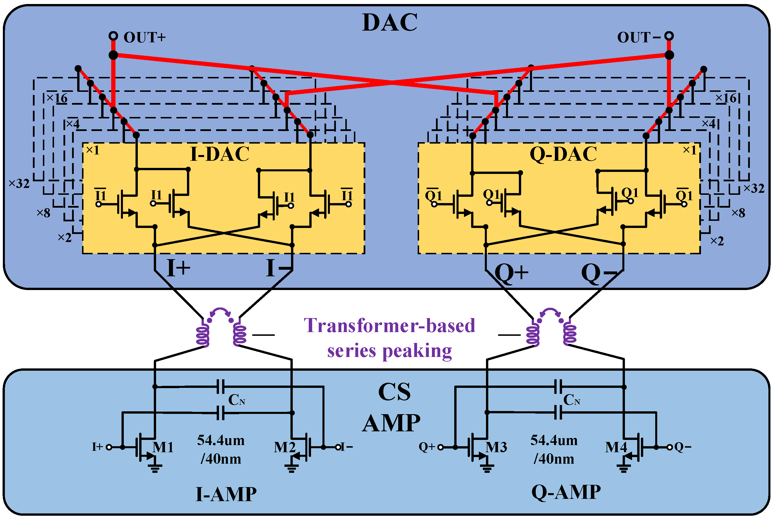
One of the core challenges in PS design is ensuring the stability of the impedance across different phase states; otherwise, it can complicate the design of the matching network. At the same time, impedance instability can alter the signal transmission characteristics, leading to phase errors. To address this issue, the transistors in the DAC array adopt a complementary switch structure [18]. As shown in Figure 5, the I/Q dual DAC array and the driving amplifier below form a cascade structure. A and B are the output control bits of the 6-bit decoder, with values ranging from 000000 to 111111. M1 to M4 are the drive amplifier transistors of the same size. Above the M1 transistor, two sets of transistors are connected. The left set is controlled by A, and the right set is controlled by A ¯ (the inverse of A), forming a complementary switch structure. Regardless of the value of A, there are always six transistors conducting and six transistors off above the M1 transistor, ensuring that the current through M1 remains stable. The principles of M2 to M4 transistors are the same, and the impedance remains unchanged under different phase states.
Figure 5. Cascade structure formed by the DAC array and the driver amplifier.
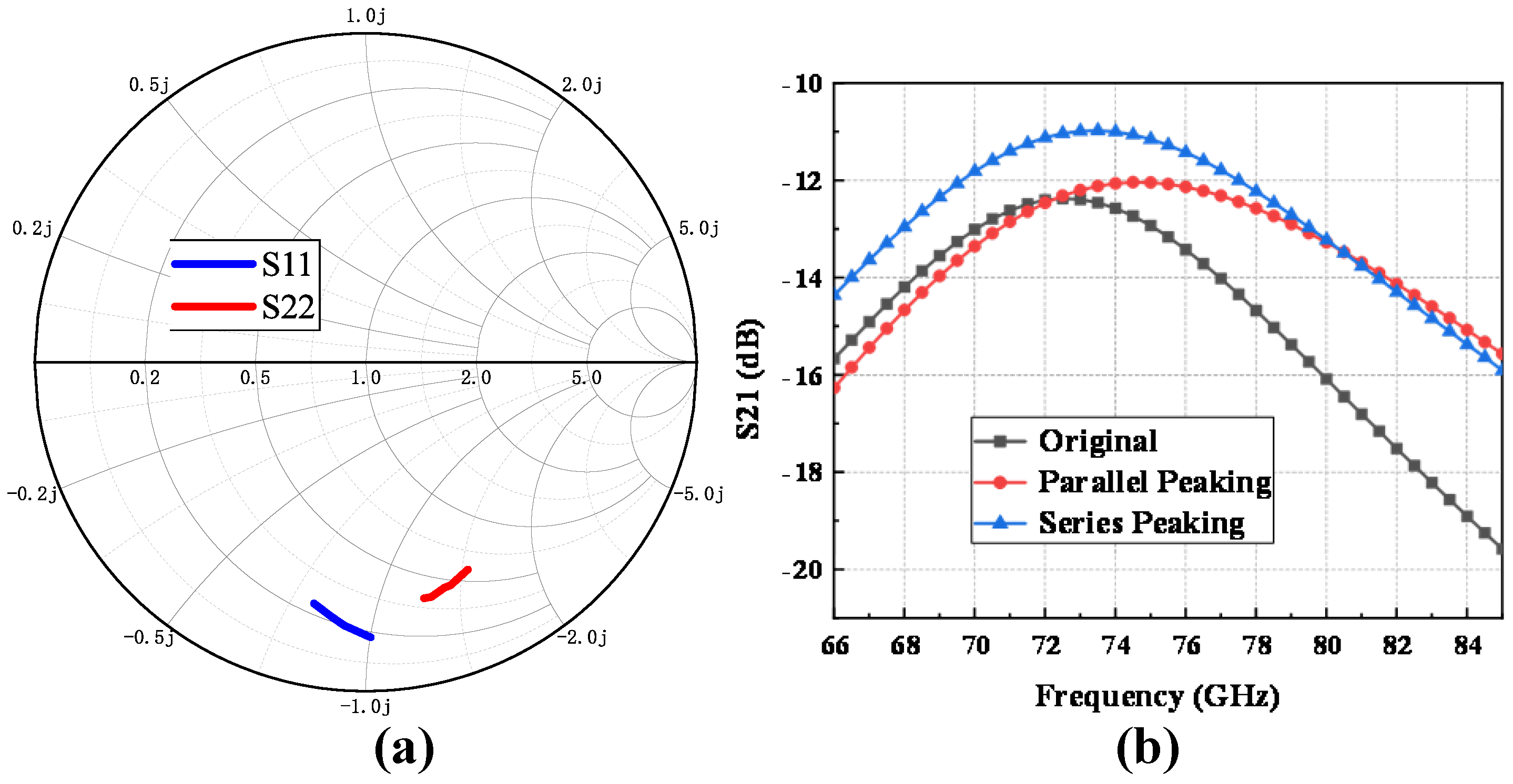
To verify the stable impedance characteristics of the complementary switch structure, a test circuit for the corresponding differential structure was set up. The I+/I− ports serve as the differential input ports, while OUT+/OUT− are the differential output ports. The logical combinations of control signals are used to achieve different phase states. Figure 6a shows the simulation results of S11 and S22 in the range of 73–83 GHz under different phase states. The results indicate that the DAC array using complementary switches maintains stable input and output impedance, which is beneficial for the design of the matching network.
Figure 6. Simulation results of (a) S11 and S22 and (b) S21 with different techniques.

2.3. Series Peaking Enhancement Technique

The schematic of the CS amplifier is shown in Figure 7. To improve stability, two neutralization capacitors are employed. While the complementary DAC structure ensures stable input and output impedance, the increased number of transistors results in a significant rise in equivalent parasitic capacitance. This, in turn, limits the phase shifter’s bandwidth and gain. To mitigate this issue, series peaking inductors are inserted between the CS amplifier and DAC array, creating a resonant circuit with the parasitic capacitance. To optimize the bandwidth, the LC resonant frequency is selected as the center frequency.
Figure 7. Circuit schematic of the CS amplifier, series inductance, and DAC array.
To verify the improvement effect of series/parallel resonance on overall bandwidth and gain, circuit validation is performed using the 77 GHz frequency band as an example. The results are shown in Figure 6b. For the 77 GHz frequency band, the 3 dB bandwidth was 7.6 GHz without inductance. When series or parallel inductance is added, the 3 dB bandwidth increases to 10 GHz and 11.4 GHz, respectively, yielding improvements of 31.5% and 50%. In this design, the series inductance option is chosen, as it not only enhances the bandwidth but also significantly optimizes the PS’s gain. The specific analysis can be concluded as follows.
(1)
Bandwidth Optimization: By adding series inductance, the 3 dB bandwidth of the PS increases from 7.6 GHz to 10 GHz, a 31.5% increase. This improvement alleviates the frequency deviation effects during testing, reducing the risk of the measured frequency deviating from the target frequency band, thereby enhancing the stability of the results.
(2)
Gain Enhancement: The introduction of series inductance significantly improves the peak gain of the PS (an increase of 1.3 dB), thus optimizing the transmitter link gain. This improvement reduces the design complexity of the subsequent power amplifier and enhances the overall link efficiency.

2.4. Driver Module Design

The schematic of the driver module is shown in Figure 8. The driver module consists of three cascaded CS amplifiers, each incorporating neutralization capacitors to ensure stability [19]. Compact transformers are employed to achieve input, interstage, and output matching. The driver module amplifies the output signal of the phase shift module by 16 dB, thereby providing sufficient signal power for the subsequent stage following the phase shifter.
Figure 8. Schematic of the driver module.

2.5. Large-Signal Simulation Results

The simulation results of the RMS phase error, large-signal gain and OP1dB for the proposed PS are shown in Figure 9. Herein, Figure 9a,b present the simulation results at 77 GHz under the condition of maximum S21, while Figure 9c shows the simulated OP1dB across different frequency bands for this state. The large-signal gain reaches 6.25 dB, and the RMS phase error remains below 2° within the normal operating input power range.
Figure 9. Simulation results of (a) RMS phase error, (b) power gain versus input power and (c) OP1dB.

2.6. Process/Temperature Variation and Monte Carlo Analysis

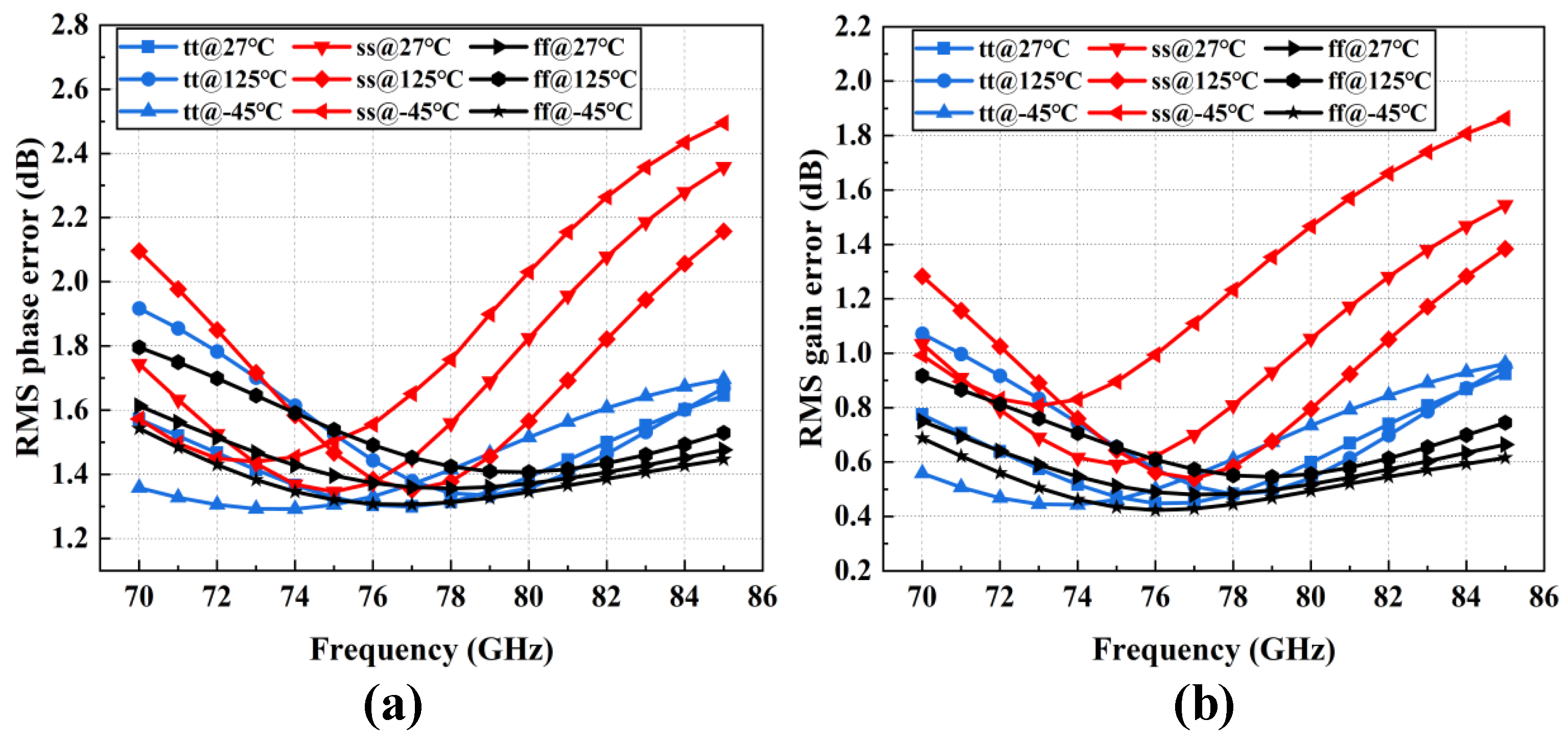
Figure 10a,b present the simulated results of the RMS phase error and RMS gain error of the proposed design under different temperatures and process corners. In every case, the RMS phase error is limited to under 2.5°, with the RMS gain error stayed below 1.9 dB.
Figure 10. The process/temperature variation in (a) RMS phase error and (b) RMS gain error.
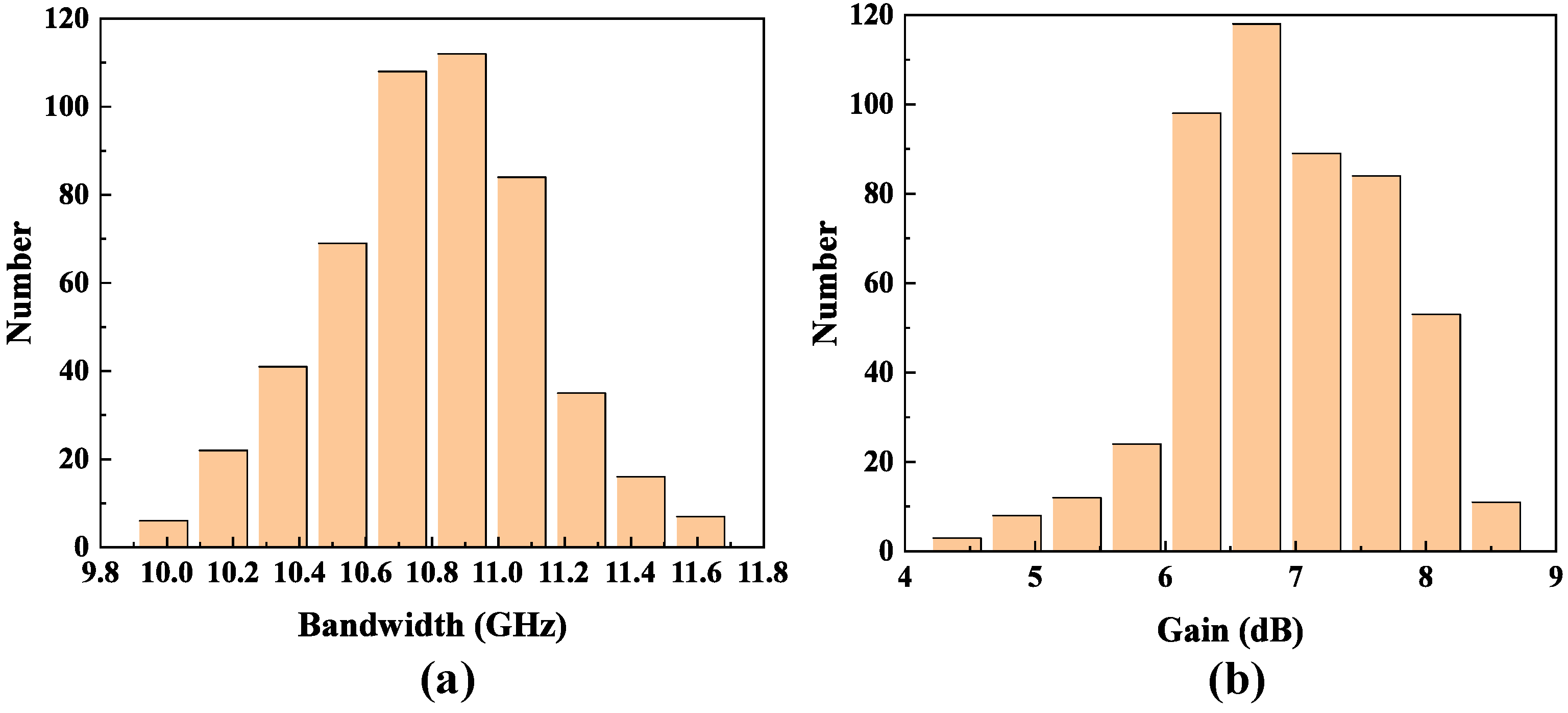
Figure 11a,b illustrate the bandwidth (BW) and gain (Gain) results obtained from 500 sample Monte Carlo simulations. It can be observed that the bandwidth exhibits a relatively concentrated performance range, remaining stable with a mean value close to 10.8 GHz. Regarding gain distribution, a large proportion of samples fall within the range of 6–8 dB, indicating a favorable degree of concentration.
Figure 11. The Monte Carlo simulation results for (a) bandwidth and (b) gain.

3. Measurement Results

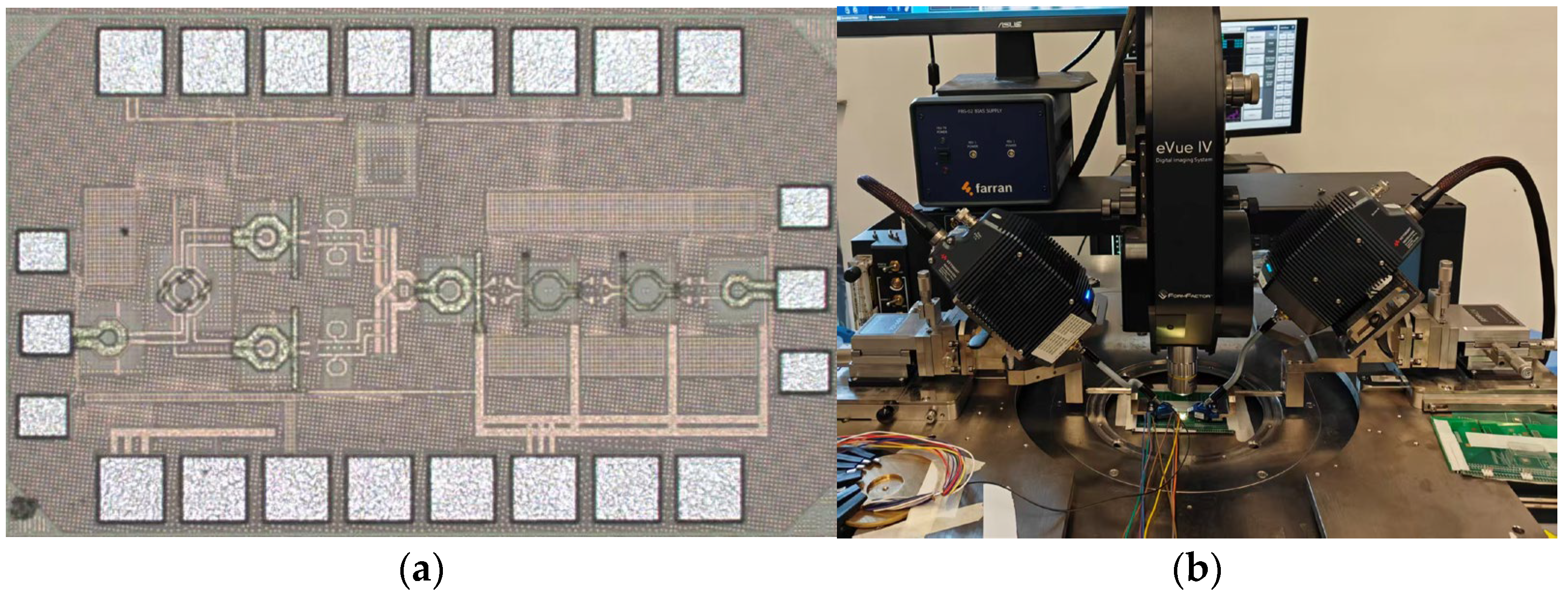
The chip micrograph of the proposed 6-bit PS is shown in Figure 12a. The design is implemented in 40 nm CMOS technology, occupying a core area of 940 µm × 280 µm. At a supply voltage of 1.1 V, the circuit draws a DC current of 52 mA, corresponding to a power consumption of 57.2 mW. Figure 12b presents the test setup for the proposed PS, utilizing a Keysight N5290A PNA Series 110 GHz millimeter-wave network analyzer, sourced from USA. First, solder the chip onto the PCB board and use gold wire bonding to connect the relevant pads to the PCB test board. Signals are transmitted via GSG probe needle contact. Before testing, verify the DC operating condition of the chip using a voltmeter and ammeter. Once confirmed normal, perform relevant calibrations, and finally test its S-parameters and large-signal performance.
Figure 12. (a) Chip photograph of the proposed 6-bit PS. (b) Test setup for the proposed PS.
The measured and simulated results are presented in Figure 13. The PS achieves a 3 dB bandwidth of 72.3 GHz to 82.3 GHz. Within this bandwidth, the measured S21 ranges from 0.5 dB to 3 dB, which is approximately 2 dB lower than the simulated values, while the measured S22 remains below −7.3 dB.
Figure 13. S parameter of the proposed PS.
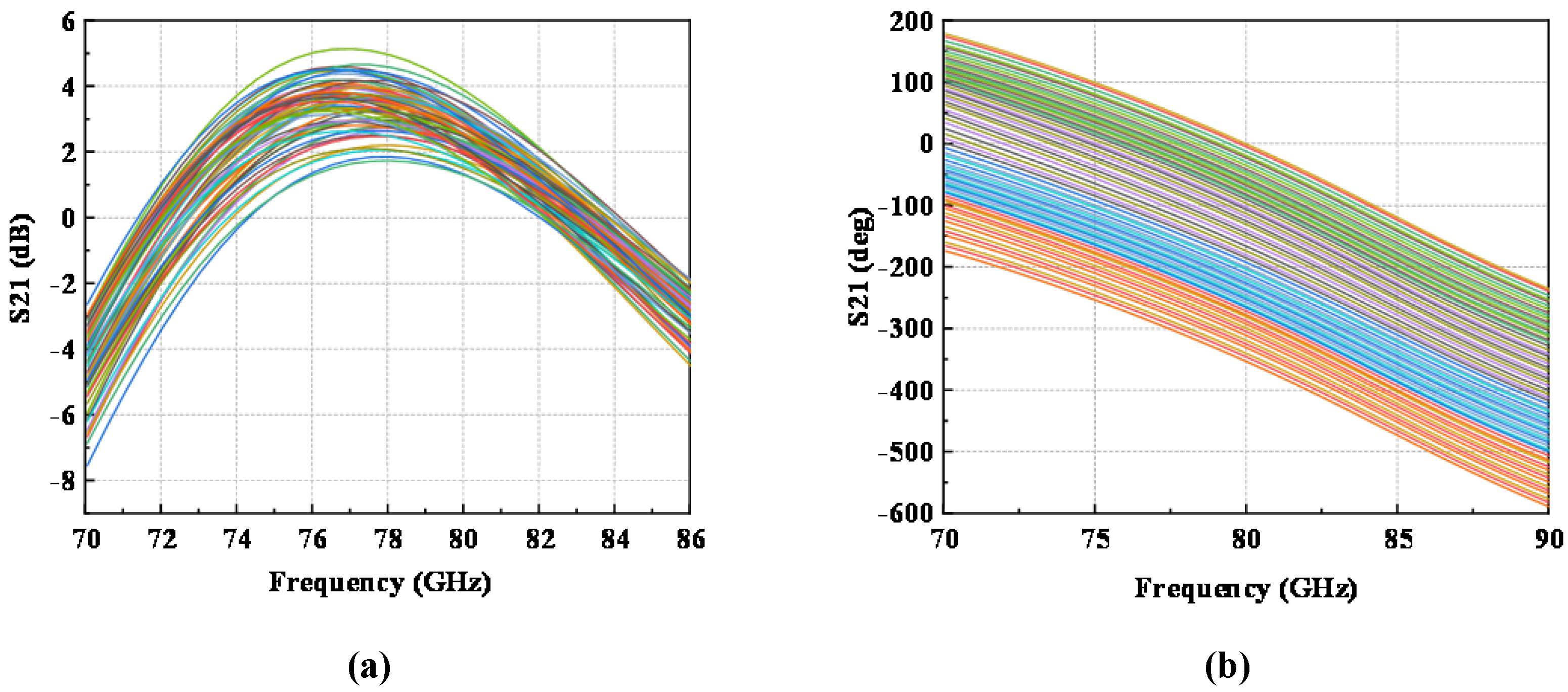
The proposed PS provides a full 360° phase-shifting range with a minimum phase resolution of 5.625°. The measured relative phase-shifting responses for all 64 states are shown in Figure 14. As illustrated in Figure 14a, the variation in S21 at 77 GHz across different phase states is 3.4 dB. Figure 14b presents the phase response of S21 for the 64 states, where minimal overlap between the phase curves is observed, indicating satisfactory phase performance.
Figure 14. The measurement results of S21 for different phase shifting states: (a) amplitude and (b) phase.
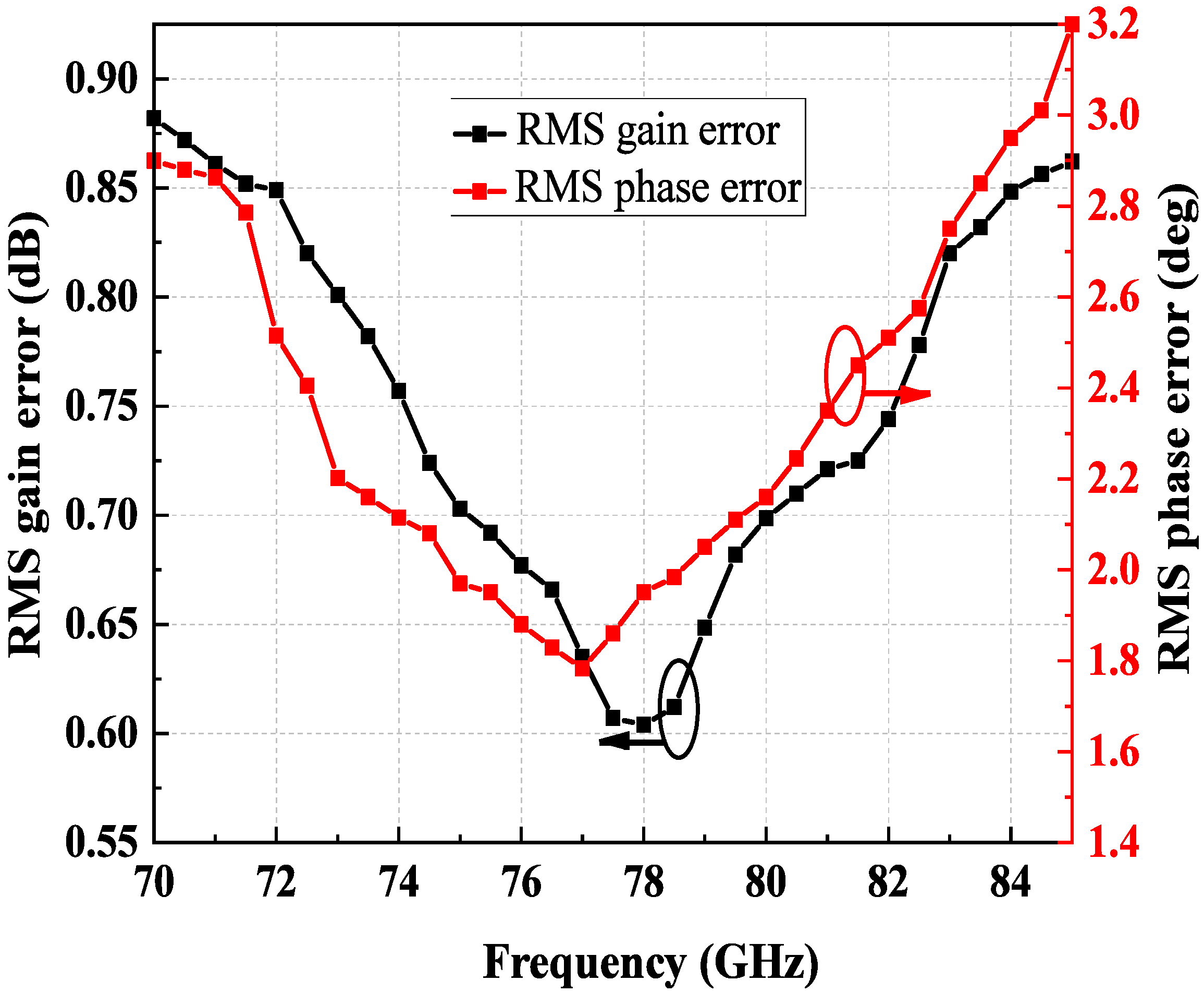
The RMS phase error and RMS gain error are summarized in Figure 15. The RMS phase error remains below 2.55° over the 72.3–82.3 GHz band, while the RMS gain error is less than 0.75 dB. Across the entire frequency range, the RMS phase error does not exceed 2.8°, meeting the 5.625° phase resolution requirement.
Figure 15. The measurement results of RMS phase error and RMS gain error.

4. Conclusions

In this paper, an E-band 6-bit high-precision active PS is proposed. The PS employs a compact capacitor-free QGC with inductive compensation to generate a high-quality quadrature signal for low RMS errors. In addition, the series peaking enhancement technique is applied to improve the operational bandwidth. The core area of the proposed PS is 940 um × 280 um. The proposed PS exhibits a measured peak gain of 5.1 dB at 77 GHz, and 3 dB bandwidth from 72.3 to 82.3 GHz. Within the 3 dB bandwidth, the RMS phase error is as low as 1.78–2.55 deg without calibration, and the RMS gain error is 0.6–0.75 dB. The performance of the PS is summarized and compared with previous mm-wave PSs in Table 1. The proposed PS offers advantages in terms of compact size and high precision, making it well-suited for large-scale phased array systems operating in the E-band.
Table 1. Performance summary and comparison to previous mm-wave PSs.

Author Contributions

Conceptualization, L.J. and B.C.; Methodology, B.C. and S.H.; Validation, L.J., B.C., S.H. and X.Q.; Formal analysis, L.J.; Investigation, X.Q.; Data curation, S.H.; Writing—original draft, L.J. and B.C.; Writing—review & editing, S.H., X.Q. and Y.W.; Visualization, L.J.; Supervision, Y.W.; Project administration, Y.W.; Funding acquisition, Y.W. All authors have read and agreed to the published version of the manuscript.

Funding

This research received no external funding.

Data Availability Statement

The original contributions presented in this study are included in the article. Further inquiries can be directed to the corresponding author(s).

Conflicts of Interest

The authors declare no conflict of interest.

References

  1. Sowlati, T.; Sarkar, S.; Perumana, B.; Chan, W.L.; Afshar, B.; Boers, M.; Shin, D.; Mercer, T.; Chen, W.H.; Toda, A.P.; et al. A 60GHz 144-element phased-array transceiver with 51dBm maximum EIRP and ±60° beam steering for backhaul application. In Proceedings of the 2018 IEEE International Solid-State Circuits Conference—(ISSCC), San Francisco, CA, USA, 11–15 February 2018; pp. 66–68. [Google Scholar] [CrossRef]
  2. Kibaroglu, K.; Sayginer, M.; Rebeiz, G.M. A Low-Cost Scalable 32-Element 28-GHz Phased Array Transceiver for 5G Communication Links Based on a 2 × 2 Beamformer Flip-Chip Unit Cell. IEEE J. Solid-State Circuits 2018, 53, 1260–1274. [Google Scholar] [CrossRef]
  3. Sadhu, B.; Tousi, Y.; Hallin, J.; Sahl, S.; Reynolds, S.K.; Renström, Ö.; Sjögren, K.; Haapalahti, O.; Mazor, N.; Bokinge, B.; et al. A 28-GHz 32-Element TRX Phased-Array IC with Concurrent Dual-Polarized Operation and Orthogonal Phase and Gain Control for 5G Communications. IEEE J. Solid-State Circuits 2017, 52, 3373–3391. [Google Scholar] [CrossRef]
  4. Zhu, W.; Lv, W.; Liao, B.; Zhu, Y.; Dai, Y.; Li, P.; Zhang, L.; Wang, Y. A 21 to 30-GHz Merged Digital-Controlled High Resolution Phase Shifter-Programmable Gain Amplifier with Orthogonal Phase and Gain Control for 5-G Phase Array Application. In Proceedings of the 2019 IEEE Radio Frequency Integrated Circuits Symposium (RFIC), Boston, MA, USA, 2–4 June 2019; pp. 67–70. [Google Scholar] [CrossRef]
  5. Trinh, K.T.; Lin, C.-H.; Kao, H.-L.; Chiu, H.-C.; Karmakar, N.C. 18–20 GHz Compact Passive 4-Bit GaAs MMIC Phase Shifter with Low Insertion Loss. In Proceedings of the 2019 IEEE Asia-Pacific Microwave Conference (APMC), Singapore, 10–13 December 2019; pp. 968–970. [Google Scholar] [CrossRef]
  6. Chen, C.-Y.; Wang, Y.-S.; Lin, Y.-H.; Hsiao, Y.-H.; Wu, Y.-C.; Wang, H. A 36–40 GHz full 360° ultra-low phase error passive phase shifter with a novel phase compensation technique. In Proceedings of the 2017 47th European Microwave Conference (EuMC), Nuremberg, Germany, 10–12 October 2017; pp. 1245–1248. [Google Scholar] [CrossRef]
  7. Tian, Y.; Gu, J.; Xu, H.; Liu, W.; Duan, Z.; Gao, H.; Yan, N. A 26-32GHz 6-bit Bidirectional Passive Phase Shifter with 14dBm IP1dB and 2.6° RMS Phase Error for Phased Array System in 40nm CMOS. In Proceedings of the 2023 IEEE/MTT-S International Microwave Symposium—IMS 2023, San Diego, CA, USA, 11–16 June 2023; pp. 195–198. [Google Scholar] [CrossRef]
  8. Li, X.; Liu, B.; Fu, H.; Ma, K. A 30–36 GHz Passive Hybrid Phase Shifter with a Transformer-Based High-Resolution Reflect-Type Phase Shifting Technique. IEEE Trans. Circuits Syst. II Express Briefs 2021, 68, 2419–2423. [Google Scholar] [CrossRef]
  9. Duan, Z.; Wang, Y.; Lv, W.; Dai, Y.; Lin, F. A 6-bit CMOS Active Phase Shifter for Ku-Band Phased Arrays. IEEE Microw. Wirel. Compon. Lett. 2018, 28, 615–617. [Google Scholar] [CrossRef]
  10. Cetindogan, B.; Ozeren, E.; Ustundag, B.; Kaynak, M.; Gurbuz, Y. A 6 Bit Vector-Sum Phase Shifter with a Decoder Based Control Circuit for X-Band Phased-Arrays. IEEE Microw. Wirel. Compon. Lett. 2016, 26, 64–66. [Google Scholar] [CrossRef]
  11. Wu, T.; Zhao, C.; Liu, H.; Wu, Y.; Yu, Y.; Kang, K. A 51.5–64.5 GHz Active Phase Shifter Using Linear Phase Control Technique with 1.4° Phase resolution in 65-nm CMOS. In Proceedings of the 2019 IEEE Radio Frequency Integrated Circuits Symposium (RFIC), Boston, MA, USA, 2–4 June 2019; pp. 59–62. [Google Scholar] [CrossRef]
  12. Zhang, X.; Deng, B.; Sun, L.; Pan, D.; Cheng, L. A W-Band 0.18-dB RMS Gain and 0.97° Phase Error Active Phase Shifter in 28-nm CMOS. IEEE Microw. Wirel. Technol. Lett. 2024, 34, 923–926. [Google Scholar] [CrossRef]
  13. Huang, D.; Zhang, L.; Li, D.; Zhang, L.; Wang, Y.; Yu, Z. A 60-GHz 360° 5-Bit Phase Shifter with Constant IL Compensation Followed by a Normal Amplifier with ±1 dB Gain Variation and 0.6-dBm OP −1dB. IEEE Trans. Circuits Syst. II Express Briefs 2017, 64, 1437–1441. [Google Scholar] [CrossRef]
  14. Xia, J.; Farouk, M.; Boumaiza, S. Digitally-Assisted 27-33 GHz Reflection-Type Phase Shifter with Enhanced Accuracy and Low IL-Variation. In Proceedings of the 2019 IEEE Radio Frequency Integrated Circuits Symposium (RFIC), Boston, MA, USA, 2–4 June 2019; pp. 63–66. [Google Scholar] [CrossRef]
  15. Huang, D.; Zhang, L.; Zhu, H.; Chen, B.; Tang, Y.; Wang, Y. A 94GHz 2×2 Phased-Array FMCW Imaging Radar Transceiver with 11dBm Output Power and 10.5dB NF in 65nm CMOS. In Proceedings of the 2019 IEEE Radio Frequency Integrated Circuits Symposium (RFIC), Boston, MA, USA, 2–4 June 2019; pp. 47–50. [Google Scholar] [CrossRef]
  16. Zhou, J.; Qian, H.J.; Luo, X. A 9-Bit Vector-Sum Digital Phase Shifter Using High Resolution VGAs and Compensated Quadrature Signal Generator. In Proceedings of the 2019 IEEE MTT-S International Microwave Conference on Hardware and Systems for 5G and Beyond (IMC-5G), Atlanta, GA, USA, 15–16 August 2019; pp. 1–3. [Google Scholar] [CrossRef]
  17. Huang, S.; Wang, Y.; Feng, G. A Compact 53–62 GHz Phase Shifter with Series Peaking Technique in 40-nm CMOS Technology. IEEE Trans. Circuits Syst. II Express Briefs 2024, 71, 4407–4411. [Google Scholar] [CrossRef]
  18. So, C.; Sung, E.-T.; Hong, S. A 60-GHz Variable Gain Phase Shifter Based on Body Floated RF-DAC Structure. IEEE Trans. Circuits Syst. II Express Briefs 2022, 69, 4749–4753. [Google Scholar] [CrossRef]
  19. Que, X.; Jiang, L.; Huang, S.; Wang, Y. A CMOS E-Band Reconfigurable Series Doherty Power Amplifier for 6-/12-dB Back-Off Efficiency Enhancement. IEEE Microw. Wirel. Technol. Letters 2025, 35, 1202–1205. [Google Scholar] [CrossRef]
  20. Pepe, D.; Zito, D. Two mm-Wave Vector Modulator Active Phase Shifters with Novel IQ Generator in 28 nm FDSOI CMOS. IEEE J. Solid-State Circuits 2017, 52, 344–356. [Google Scholar] [CrossRef]
  21. Jang, J.; Kim, B.; Kim, C.-Y.; Hong, S. 79-GHz Digital Attenuator-Based Variable-Gain Vector-Sum Phase Shifter with High Linearity. IEEE Microw. Wirel. Compon. Lett. 2018, 28, 693–695. [Google Scholar] [CrossRef]
  22. Park, G.H.; Byeon, C.W.; Park, C.S. A 60-GHz Low-Power Active Phase Shifter with Impedance-Invariant Vector Modulation in 65-nm CMOS. IEEE Trans. Microw. Theory Tech. 2020, 68, 5395–5407. [Google Scholar] [CrossRef]
  23. Sung, E.-T.; Wang, S.; Hong, S. A 60-GHz Polar Vector Modulator with Lookup Table-Based Calibration. IEEE Microw. Wirel. Compon. Lett. 2021, 31, 572–574. [Google Scholar] [CrossRef]
  24. Quan, X.; Yi, X.; Boon, C.C.; Yang, K.; Li, C.; Liu, B.; Liang, Z.; Zhuang, Y. A 52–57 GHz 6-Bit Phase Shifter with Hybrid of Passive and Active Structures. IEEE Microw. Wirel. Compon. Lett. 2018, 28, 236–238. [Google Scholar] [CrossRef]
Disclaimer/Publisher’s Note: The statements, opinions and data contained in all publications are solely those of the individual author(s) and contributor(s) and not of MDPI and/or the editor(s). MDPI and/or the editor(s) disclaim responsibility for any injury to people or property resulting from any ideas, methods, instructions or products referred to in the content.

Article Metrics

Citations

Article Access Statistics

Multiple requests from the same IP address are counted as one view.