1. Introduction
In the implementation of today’s System-on-Chip (SoC) and Network-on-Chip (NoC) designs, shared communication buses and their arbiters function as essential building blocks. Efficient arbitration for shared communication resources is paramount in these designs, directly impacting system performance metrics like latency and throughput [
1,
2]. Whereas conventional arbitration schemes such as fixed-priority, round-robin, crossbar switches, or static Time Division Multiple Access (TDMA), present various trade-offs concerning simplicity, efficiency, determinism, and cost [
3,
4], dynamic TDMA (dTDMA) offers a compelling balance for equally distributed loads. By dynamically allocating time slots based on real-time demand, dTDMA can achieve a more efficient bus utilization and responsiveness compared to other static schemes, without the overhead of static approaches or crossbars switches, making it suitable for systems with variable traffic patterns [
5].
A significant body of dTDMA research exists within the wireless communications domain [
6,
7]. However, architectural assumptions due to the different channel requirements (wireless vs. wired), design constraints (e.g., signal integrity, power, area, and latency), and implementation platforms (e.g., CMOS logic versus FPGAs/DSPs) for on-chip digital buses differ fundamentally from those in wireless environments, rendering direct adoption of wireless dTDMA solutions inappropriate for SoCs. According to our research on the state of the art for the last decade, there are no other published circuit-level implementations of digital dTDMA architected for general-purpose synchronous digital buses, except for the one presented by Nicopoulos et al. in [
8].
This paper addresses an architectural enhancement of the dTDMA arbitration scheme by presenting a novel, area and power-efficient solution, based on a Selectable Sequence Counter (SSC) tailored for on-chip digital bus systems. The proposed design is evaluated against the available digital dTDMA circuit implementation in [
8], and the findings demonstrate significant improvements in resource efficiency and scalability. Note that dTDMA functionality is preserved with our arbiter architecture with respect to the reference solution, and therefore tradeoffs with respect to other buses implementation hold, as discussed in [
8]. The key contributions of this paper are:
A novel arbiter circuit architecture: we present a detailed, circuit-level implementation of a dTDMA arbiter based on a Selectable Sequence Counter (SSC), a design not previously published for on-chip buses.
Linear scalability of the proposed arbiter architecture: the design demonstrates nearly linear growth in area and power as the number of connected devices increases, a significant improvement over the quadratic scaling shown by the reference architecture.
Validation and evaluation against the reference architecture available in the literature: We provide post-place-and-route simulation results for area and power on a 65 nm CMOS process, showing substantial resource savings compared to the only relevant implementation available in the literature.
The remainder of this paper is organized as follows.
Section 2 reviews existing alternatives for dTDMA bus implementations and further justifies the use of [
8] as the most recent work of reference.
Section 3 details the proposed SSC-based dTDMA system.
Section 4 presents the evaluation methodology and results.
Section 5 gathers the main findings of this work.
2. Alternatives for the Implementation of dTDMA Buses
Several approaches to dTDMA for intra-chip communication buses have been explored in the literature. These can be broadly categorized by their arbitration mechanisms, such as centralized arbiters employing scheduling algorithms [
9] or distributed schemes where masters participate in slot allocation, for instance, using feedback shift registers [
5]. Such dynamic allocation is particularly noted in hybrid buses used in NoC architectures, where dTDMA can serve as an efficient link implementation, for example, in 3D NoCs [
10].
Several optimizations and variations have also been proposed in the past. For 3D integrated circuits, specialized TDMA-based solutions like asynchronous TDMA (A-TDMA) and resonant synchronous TDMA (RS-TDMA) have been reported to manage clock distribution and enhance bandwidth [
11]. Pipelined bus structures have been suggested as alternatives or complements to dTDMA in multi-layer SoCs and for inter-layer communication in 3D NoCs to reduce arbitration complexity [
5,
12]. Furthermore, low-power dTDMA implementations, often incorporating techniques like clock gating, are crucial for energy-constrained SoCs [
5].
Recent advances in on-chip interconnects also include sophisticated budget-based arbitration mechanisms for protocols such as AXI, aiming to provide fairness and predictability, such as AXI-REALM, which uses periodic time windows and transfer fragmentation [
13]. These developments highlight ongoing efforts to manage shared on-chip resources effectively.
Yet, a survey of recent literature did not produce any detailed, replicable circuit-level implementations of general-purpose dTDMA arbiters for standard on-chip digital buses, nor were references to prior implementations found, except for minor variations to the one presented in [
8]. Though there are existing studies that present algorithmic analyses, high-level performance models, or target specialized applications (e.g., specific 3D inter-layer links), no one presented a novel digital circuit design for general bus arbitration.
Consequently, the circuit-level dTDMA arbiter implementation given in [
8] keeps being the most significant and recent reference available for benchmarking. This architecture is representative of a standard shift-register-based approach and is thoroughly documented, allowing for a direct and insightful comparison of hardware metrics. Its selection as a reference framework for high-performance computing research further validates its use as a benchmark for evaluating the practical viability of new dTDMA arbiter designs like the one presented in this paper.
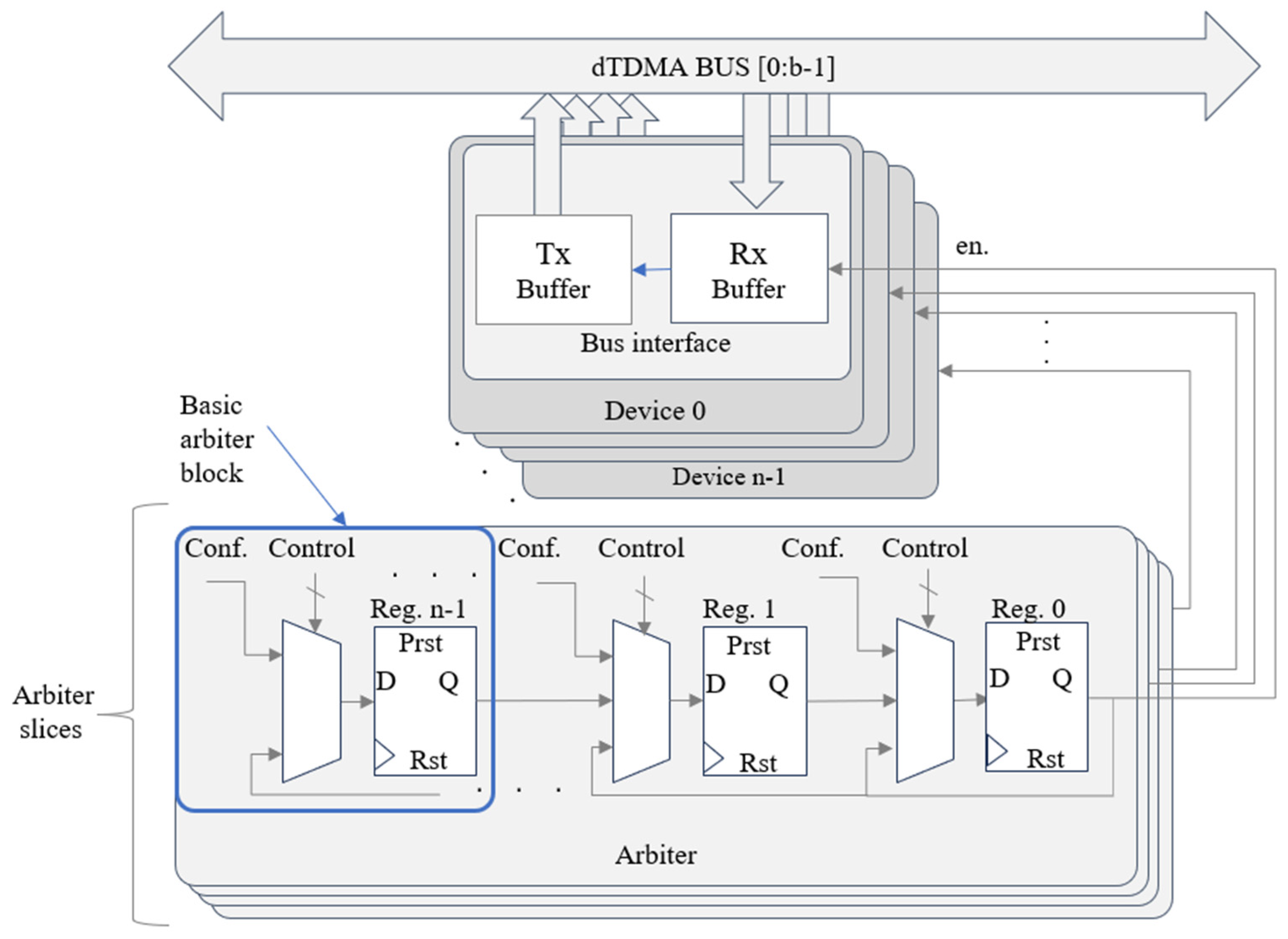
Figure 1 depicts the high-level representation of the architecture proposed in [
8].
As illustrated in
Figure 1, expanding the bus to support an additional device requires two modifications to the arbitration logic. First, a new basic arbiter block, identical to the one delineated by the blue box, must be integrated into each existing arbiter slice. Second, a new arbiter slice must be instantiated for the newly added device. The architecture then requires one arbiter slice for each device connected to the bus, and each slice must contain a basic arbiter block for every device. Consequently, for a system with n devices, the arbitration hardware comprises n slices, each containing n basic blocks. This relationship dictates that the area complexity of the arbitration logic scales quadratically with the number of devices, resulting in an overall complexity of O(n
2).
3. Proposed Implementation
The proposed dTDMA system is centered around a novel SSC arbiter. Conceptually, the arbiter operates in a two-stage process for each arbitration cycle:
Request gathering: the arbiter identifies all devices that have data to send by reading the Pending_n signals.
Sequence generation: the arbiter then dynamically builds a custom, in-order counting sequence that includes only the IDs of the requesting devices. This allows the bus to grant access sequentially just to the active requesters, skipping over any idle devices and maximizing bandwidth. The following sections detail the circuit-level implementation of this strategy.
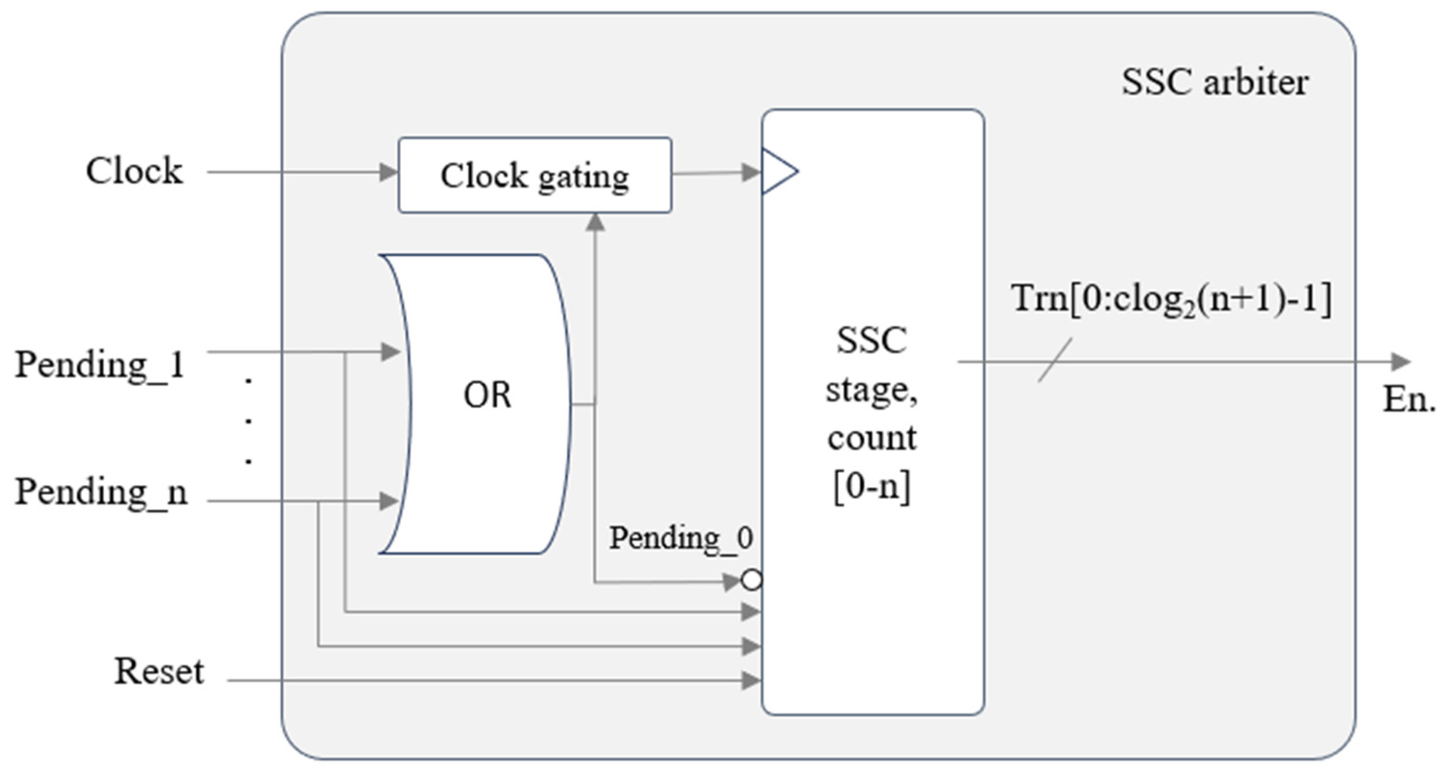
The proposed bus implementation, based on an SSC arbiter, is presented in
Figure 2. Each device connected to the bus features an independent interface consisting of the following signals.
Tr_n: a binary vector output from the arbiter indicating the ID of the device currently granted access to transmit data.
Data_in_n: a bidirectional data bus through which all devices communicate. If device n is granted access (i.e., Tr_n points to n) and has data to transmit, it uses this interface to send information.
Pending_i: a signal vector where each bit corresponds to a device. A device asserts its respective bit to indicate that it has pending data to transmit.
Full_n/Full: internally used signals indicating that a device’s FIFO is full, in which case data transmission is paused until space becomes available.
The SSC arbiter implementation uses clock gating logic that disables counting when no devices request data transmission. Note this is a functional requirement and in this scope the clock gating is not only intended for power consumption reduction. This logic is shown in
Figure 3. Devices assert the corresponding bit in the
Pending_n vector to indicate the presence of data in their output FIFOs.
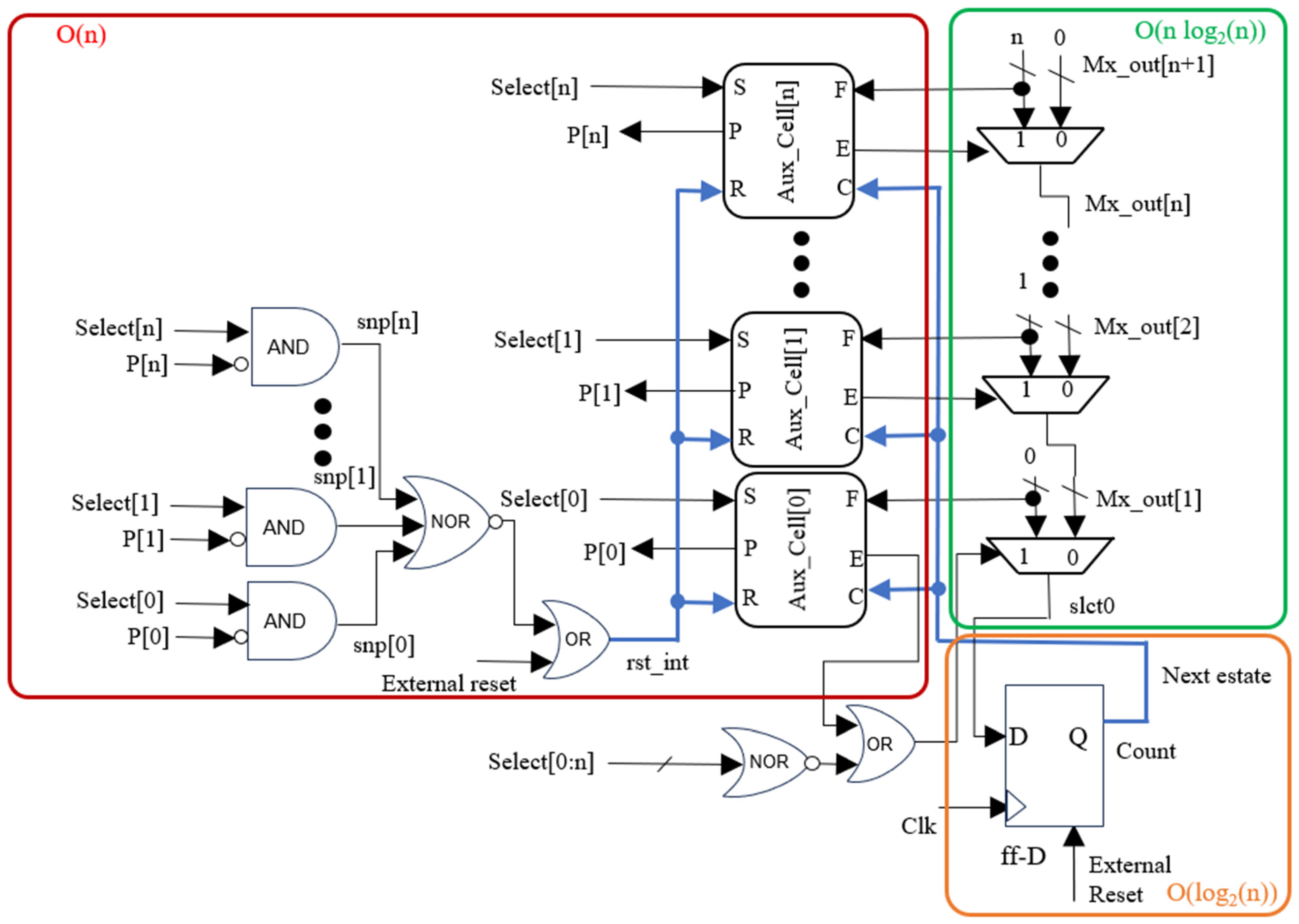
The core component of the proposed dTDMA arbiter, is the SSC stage shown in
Figure 4. This block operates as a binary, configurable, in-order counter ranging from 0 to n. From an external perspective, it differs from a traditional counter due to the inclusion of additional selection inputs, labeled
select in
Figure 4, which correspond to values from 0 to n. When asserted, these inputs define the custom sequence the counter will follow. If no selection inputs are active, the counter output (labeled
count in the figure) remains at zero. The count output provides the
Trn[0:clog2(n + 1) − 1] after being decoded, where c log is the ceiling of log
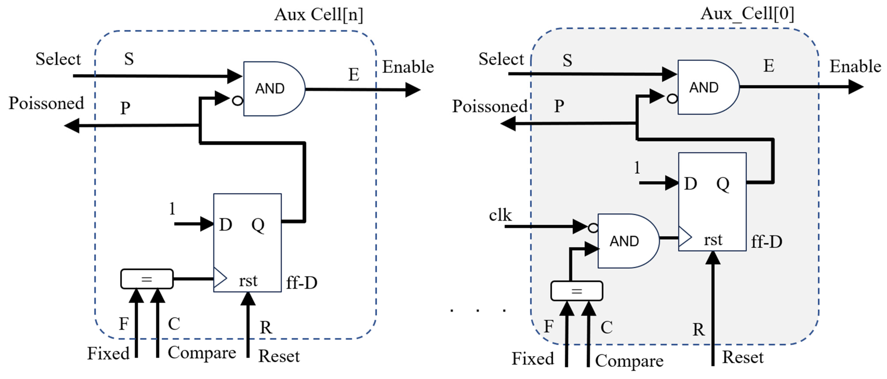
2 function. The internal structure of the auxiliary cells (
Aux_cell) used in the SSC is shown in
Figure 5. There are n + 1 auxiliary cells in the design, one for each possible value in the counting sequence plus the rest state.
Each auxiliary cell is responsible for tracking whether its corresponding value has been requested for inclusion in the sequence and whether it has already been counted. Each cell contains at least three inputs and two outputs, described as follows.
Input select (S): indicates that the associated value should be included in the sequence.
Input reset (R): resets the cell state, signaling the start of a new sequence.
Input fixed (F[0:clog2(n + 1) − 1]): a compiled-time constant that uniquely identifies the value tracked by this auxiliary cell. For example, if this value is 2, the cell tracks the inclusion of item 2.
Input compare (C[0:clog2(n + 1) − 1]): provides feedback with the current value in the sequence.
Output poisoned (P): indicates that the item has already been counted in the current sequence.
Output enable (E): signals that the item is both requested and not yet included in the sequence.
Each time the current count matches the fixed input F of an auxiliary cell (i.e., the cell’s ID), the internal flip-flop is set, indicating the item has been counted. Consequently, the enable output is de-asserted, and the next item in the sequence can be captured on the next positive clock edge. Once all selected items have been processed, all auxiliary cells are reset to initiate a new sequence.
This reset is triggered by the
rst_int signal, as depicted in
Figure 4. If no items are selected, the counter output remains at zero. This design assumes that the reset and selection signals are synchronized with the positive edge of the clock, allowing one clock cycle for the combinational logic to determine the next state.
A special case exists for item zero. Since the default state of the counter is zero, both during and after reset, the auxiliary cell for item zero (
Aux_Cell[0] in
Figure 5) includes an additional clock input. This ensures that when item zero is part of the selected sequence, it remains valid for one full cycle following reset.
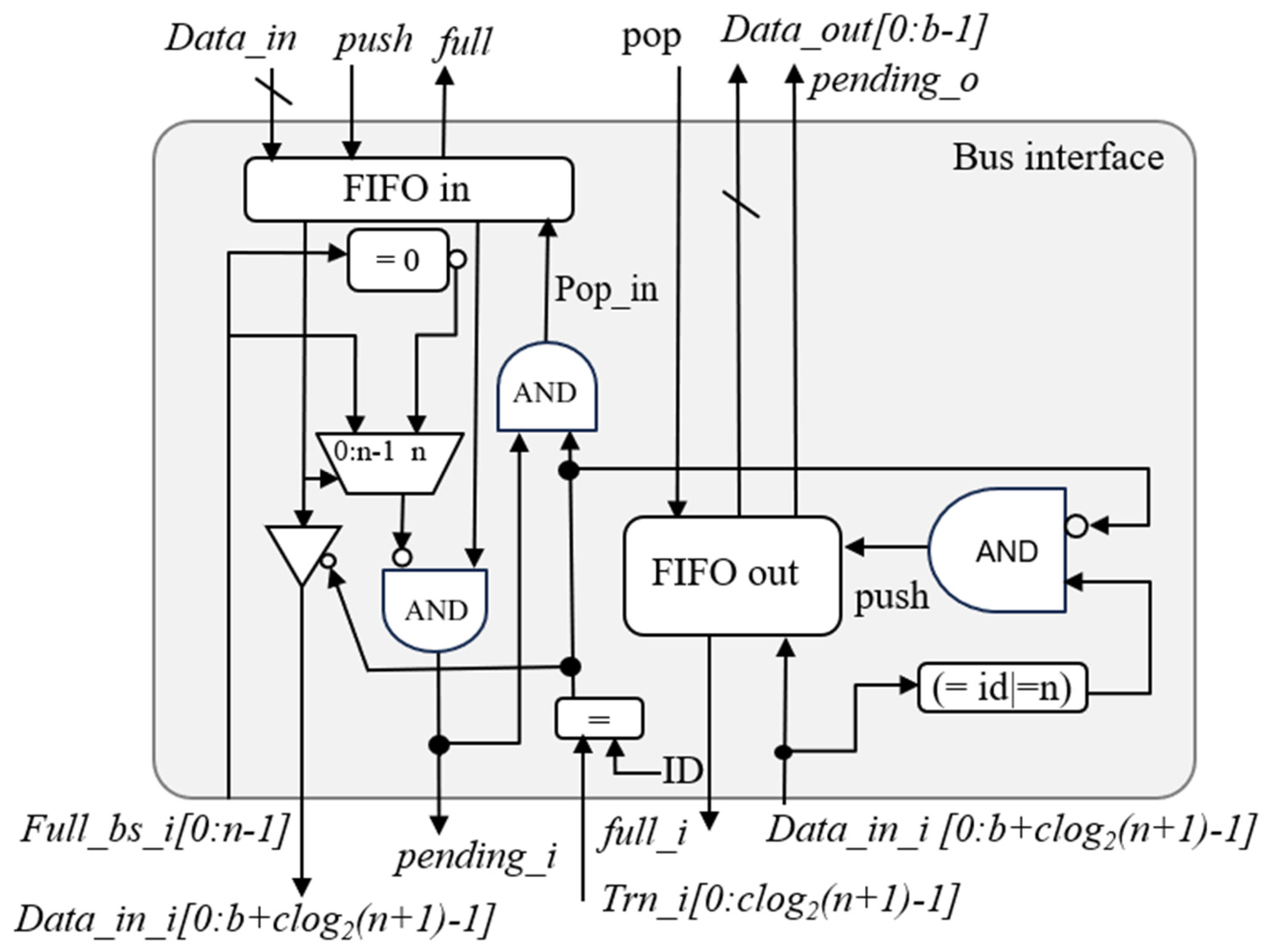
Each bus interface can be implemented using two standard FIFO structures, additional logic gates, and tri-state buffers, as illustrated in
Figure 6 with a simplified diagram.
To illustrate the SSC’s operation, consider a simplified 4-device system (n = 4). Assume devices 0, 2, and 3 request access, so the Pending vector is 4′b11010.
- 3.
Initialization: the Select[1], Select[3], and Select[4] inputs to their respective auxiliary cells are asserted. All poisoned outputs are low.
- 4.
First Timeslot (Device 0): the multiplexer logic (
Figure 4) identifies the lowest-indexed active cell, which is
Aux_Cell[1]. The counter output (Count) becomes ‘1’, granting access to Device 0.
- 5.
“Poisoning” Device 0: once the counter output matches the cell’s ID, Aux_Cell[1] sets its internal flip-flop. This causes flip-flop poisoned output to go high and its enable signal to go low. The device is now excluded from the sequence for the rest of this cycle.
- 6.
Second Timeslot (Device 2): on the next clock edge, the multiplexer logic scans for the next active, non-poisoned cell. It bypasses Aux_Cell[2] (which is not selected) and finds Aux_Cell[3]. The counter output becomes ‘3’, granting access to Device 2.
- 7.
Third Timeslot (Device 3): The process is repeated. Aux_Cell[3] is poisoned. The logic finds the next active requester, Aux_Cell[4], and the counter output becomes ‘4’.
- 8.
Sequence Reset: after Device 3 has been served, the logic detects that all selected items have been processed, triggering the internal reset (rst_int). The poisoned flip-flops in all cells are cleared, and the arbiter is ready for a new set of pending requests.
As detailed in
Figure 4, the design comprises three components with distinct area scaling characteristics. The hardware delineated by the red box exhibits linear growth (O(n)), as each additional device requires one
aux_cell and a small number of discrete gates. The component in the green box has a complexity of O(nlog
2n); this is because each new device adds a multiplexer, and the area of an n-to-1 multiplexer scales logarithmically. Finally, the counter in the orange box scales logarithmically (O(log
2 n)) with the number of devices.
In practice, the number of devices sharing a bus is typically small (i.e., n < 10) to prevent excessive division of the communication bandwidth. Within this constraint, the linear component (red box) is the dominant contributor to the total area of the design. Although the architecture contains elements with different growth rates, the contributions from the O(nlog2 n) (green) and O(log2n) (orange) components are not rival the linear term for a small device count. Therefore, the total area of the design is projected to scale in a practically linear fashion for typical configurations.
4. Evaluation of the Proposed dTDMA Implementation
The evaluation of the proposed dTDMA bus implementation was conducted using Synopsys EDA tools on a 65 nm CMOS commercial process.
To ensure a direct and unbiased comparison, both the newly introduced dTDMA architecture and the reference implementation, detailed in [
8] and adopted in several other works [
5,
9,
10], were synthesized using the same standard cell libraries. The data flit width was consistently set to 64-bit for all experiments. Logic synthesis was carried out using Synopsys Fusion Compiler [
14]. The reported area and power values were derived from post-place-and-route simulations. This considers the physical layout of the circuit, including the placement of components and the routing of interconnections, which significantly impacts the final area and power characteristics. To isolate the performance of the core bus logic, the area contribution of input/output (I/O) pads was excluded from the measurements.
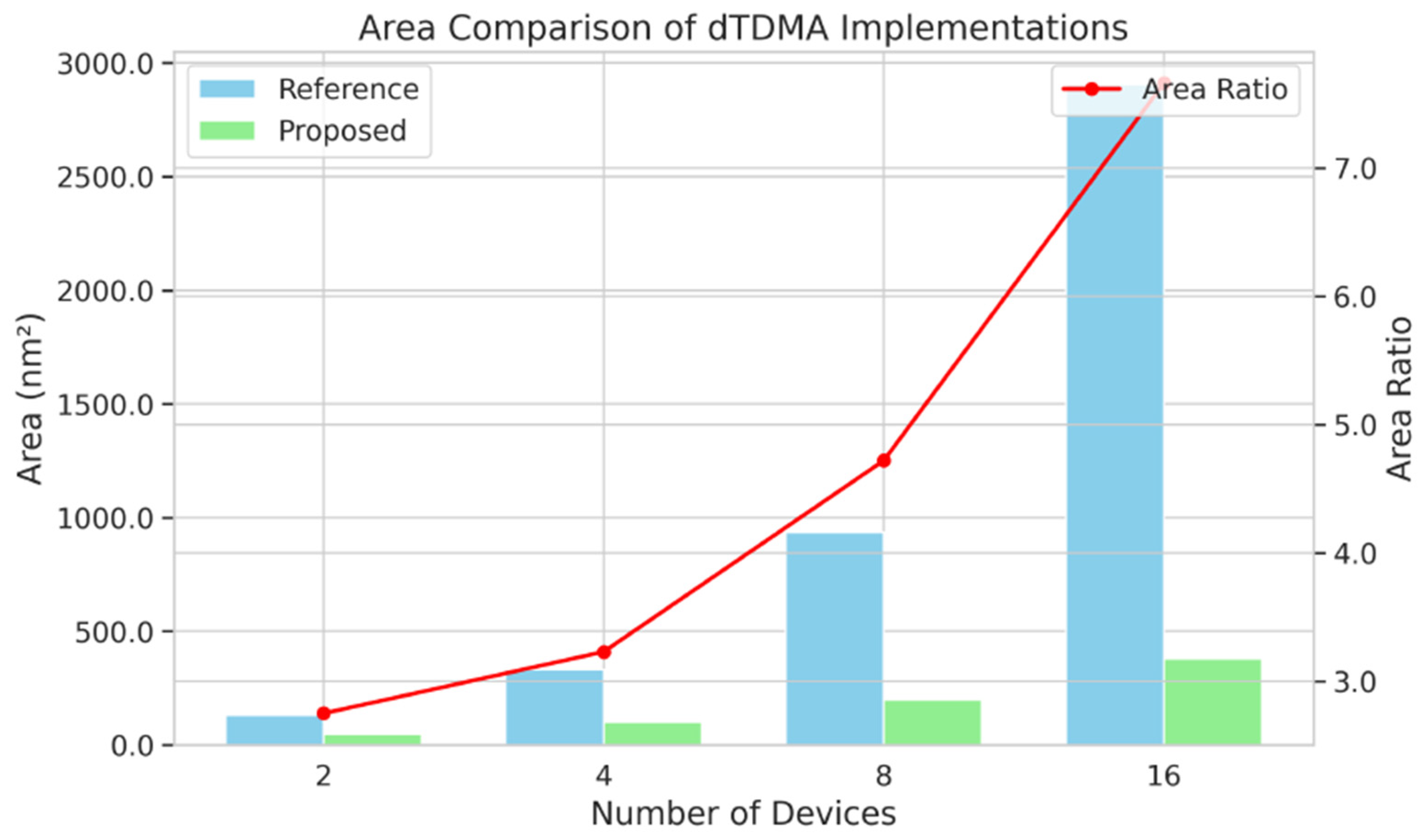
To assess the scalability of both dTDMA implementations, synthesis was performed for varying numbers of connected devices: 2, 4, 8, and 16. In this study, each connected device is implemented with FIFOs that emulate data traffic through the bus. This parametric analysis allows for an understanding of how the area requirements of each architecture evolve as the complexity of the system increases. The quantitative results of this area comparison are summarized in
Table 1 and visually represented in the bar chart of
Figure 7, providing both tabular and graphical insights into the area efficiency of the proposed design versus the reference implementation.
To evaluate power consumption under realistic operational scenarios, a SystemVerilog Universal Verification Methodology (UVM) [
15] environment was developed. This testbench was specifically designed to mimic typical data communication patterns within SoC. It generated randomized transactions, involving the transfer of random data packets between randomly selected devices connected to the bus. This dynamic traffic generation enabled the capture of detailed waveform data, tracking the signal transitions of all nodes within the design over a simulated period.
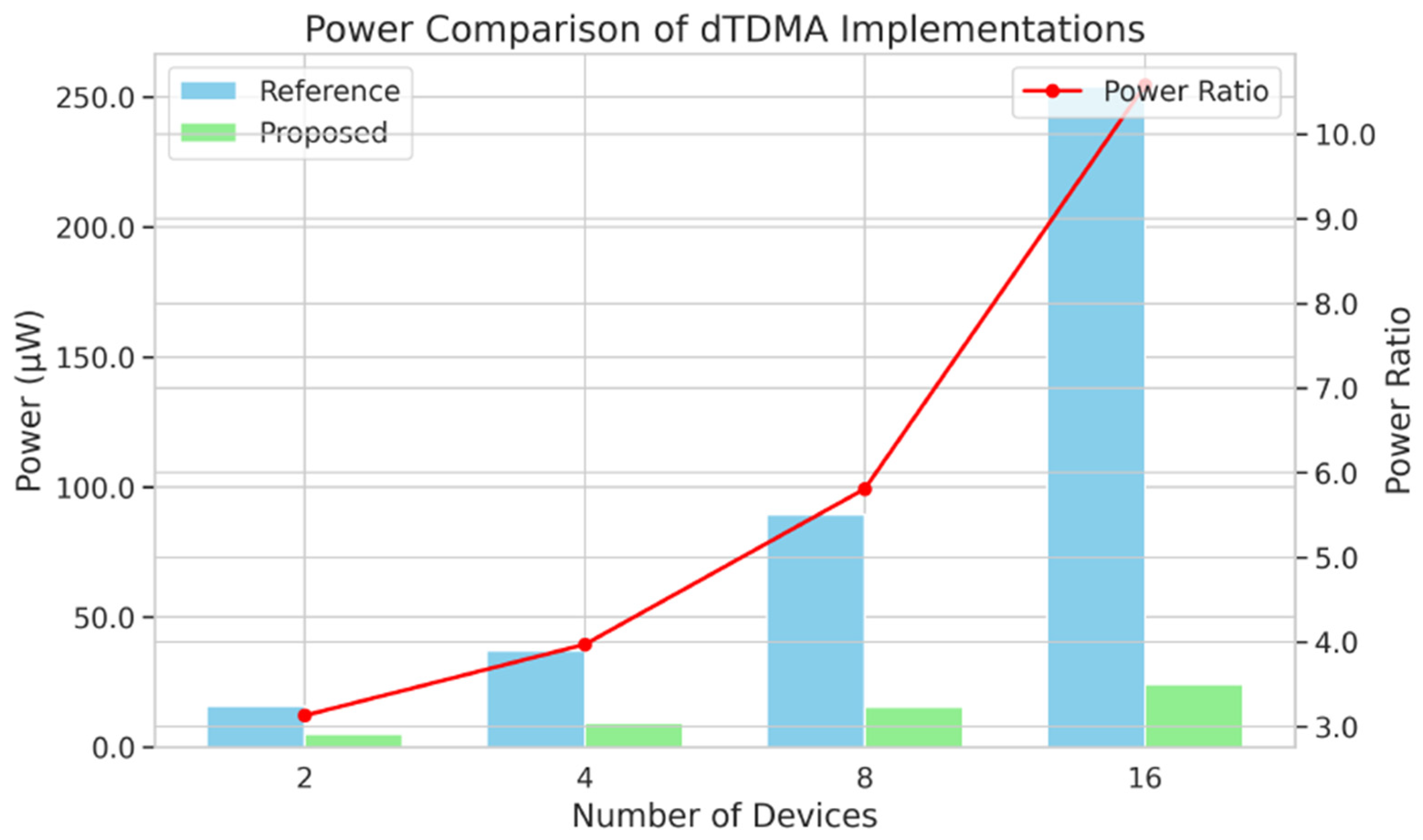
The captured waveform data was subsequently processed to generate a Switching Activity Interchange Format (SAIF) file. The SAIF file contains statistical information about the switching frequency of each node in the circuit, providing a realistic profile of the design’s dynamic behavior. This SAIF file was then imported back into Synopsys Fusion Compiler during the power analysis phase. By applying these activity factors, the power estimation closely reflects the actual power dissipated during typical operation. To ensure a fair and consistent comparison, the exact same UVM-based verification testbench and the resulting SAIF files were used for power analysis of both the proposed and the reference dTDMA implementations for each system configuration (2, 4, 8, and 16 devices, each with a 64-bit flit width). The multiple power reports generated for each configuration were then compiled and are presented in
Table 2 and visualized in
Figure 8, allowing for a direct comparison of the power efficiency of the two approaches across different system sizes. The analysis of the results demonstrates a significant advantage of the proposed design in terms of both area and power. The reference design exhibits a non-linear, close to quadratic, increase in area with the number of devices, which is attributed to its underlying architectural scaling where both the horizontal and vertical dimensions of the bus expand with each added device. In contrast, the proposed solution demonstrates a much more favorable nearly linear growth in area, leading to a considerably smaller physical footprint, especially as the number of connected devices becomes larger. This difference in area scaling has profound implications for the scalability of the system, with the reference design becoming increasingly area-inefficient for larger-scale integrations.
A similar trend is observed in power consumption metrics. The reference design consistently consumes substantially more power than the proposed solution, often approaching or exceedingly twice the power dissipation. This higher power consumption is strongly correlated with the larger area occupied by the reference design. A larger physical area typically implies longer interconnects, which contribute to increased parasitic capacitance. Furthermore, a greater number of active components within a larger area leads to higher switching activity and increased leakage currents. The compound effect of these factors results in significantly elevated power consumption observed in reference architecture compared to the more compact proposed implementation.
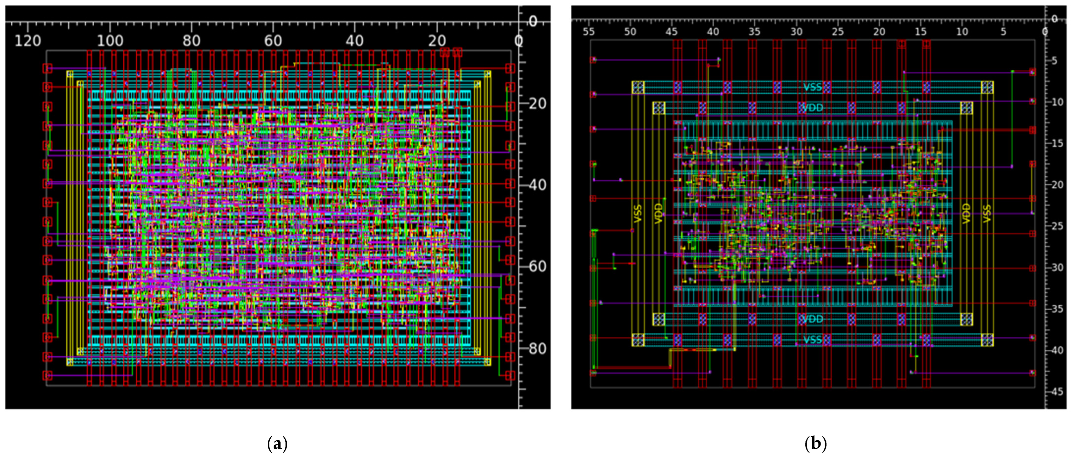
Figure 9 shows the comparative layout view for the reference solution vs. the proposed solution for 16 devices connected, with a roughly 5 times less footprint area requirement when considering full cell size with power rails and ring pads.
5. Conclusions
This paper has presented a novel and efficient balanced dTDMA bus architecture, based on a new SSC arbitration circuit. Through the evaluation and comparison against a conventional dTDMA implementation from the literature, using a 65 nm CMOS process, the proposed design has shown significant advantages across key performance metrics.
Post-place-and-route simulation results reveal that the presented arbiter consistently achieves lower area consumption and power dissipation compared to the only available baseline architecture in the literature. Notably, the area of the proposed design scales nearly linearly as a function of the number of connected devices, instead of quadratically, as the reference design. This leads to substantial area savings, particularly in larger systems. Similarly, power analysis based on realistic switching activity indicates that the proposed implementation consumes significantly less power, with the power ratio between the reference and proposed designs increasing with the number of devices. These findings underscore the effectiveness and resource efficiency of the proposed dTDMA bus architecture, making it a competitive alternative for the design of high-performance and energy-aware on-chip communication systems in future SoCs and NoCs. The modularity of the proposed SSC-based arbiter also suggests potential benefits in terms of design complexity and ease of integration. Future work could explore the latency characteristics of the proposed design under various traffic patterns and investigate its adaptability to different NoC topologies and QoS requirements.
