Communication

Experimental Evaluation of Coupled-Line Tunable Inductors with Switchable Mutual Coupling

1
Department of Intelligent Semiconductors, Soongsil University, 369, Sangdo-ro, Dongjak-gu, Seoul 06978, Republic of Korea
2
Department of Electric Engineering, Soongsil University, 369, Sangdo-ro, Dongjak-gu, Seoul 06978, Republic of Korea
*
Author to whom correspondence should be addressed.
Electronics 2025, 14(16), 3228; https://doi.org/10.3390/electronics14163228
Submission received: 12 July 2025 / Revised: 12 August 2025 / Accepted: 13 August 2025 / Published: 14 August 2025

Abstract

This paper investigates and characterizes a tunable inductor structure based on coupled-line configurations, referred to as a coupled-line tunable inductor (CLTI). By integrating switches along the coupled-line paths, the mutual inductance can be selectively enabled or disabled, providing a means for active inductance modulation. Spiral inductors with one-turn and two-turn cores were used in conjunction with inner-coupled-line placements to explore different coupling configurations. The test structures were implemented using printed circuit board (PCB) technology, and their performance was analyzed through electromagnetic simulations and vector network analyzer (VNA) measurements. The results confirm that switch-controlled coupled lines enable effective inductance tuning, with a measurable reduction in inductance when the coupled-line path is activated. In the switch-OFF state, only minimal performance degradation was observed due to parasitic effects. These findings provide useful insights into the practical behavior of coupled-line tunable inductors and suggest their applicability in RF circuits and adaptive analog systems, particularly where integration and compact tunability are desired.

1. Introduction

In recent years, the rapid advancement of wireless communication technologies has fueled growing demands for ultra-high-speed data transmission across a wide range of applications, including autonomous vehicles, virtual reality (VR), and 5G/6G mobile networks [1,2,3,4,5,6]. In response, significant attention has been directed toward circuit components that support dual-band operation and frequency agility, enabling flexible use of spectral resources while maintaining precise electrical characteristics [5,6,7,8,9,10,11]. These evolving requirements underscore the necessity for tunable circuit elements that can adapt to increasingly diverse communication environments and complex system specifications.
Among the various tunable components, resistive and capacitive elements have been extensively studied and utilized. As illustrated in Figure 1, tunable resistors typically employ MOSFETs operating in the triode region or BJTs in the saturation region to modulate on-resistance, serving essential roles in circuits such as variable-gain amplifiers [12,13,14]. Varactors, which adjust capacitance by controlling the depletion width of a reverse-biased PN junction, are commonly used in voltage-controlled oscillators and resonant circuits [15,16,17]. These components have proven effective in supporting key functions such as frequency tuning, gain control, and mode switching in high-frequency integrated circuits (ICs).
In comparison, the development of tunable inductors has progressed at a relatively slower pace, despite their critical importance in RF and microwave circuits [18]. Inductors contribute not only to passive energy storage but also to core RF functionalities, including impedance matching, bandpass filtering, and oscillator design. Since the inductance value directly influences key circuit metrics such as resonance frequency, quality factor (Q), and bandwidth, the ability to dynamically tune inductance is desirable for enhanced design flexibility and performance optimization [19,20]. However, achieving tunability in inductors—while maintaining low loss, compact size, and manufacturability—remains a challenging task [11].
Existing approaches to inductance tunability have explored microelectromechanical systems (MEMSs), semiconductor-based electromagnetic coupling, and reconfigurable resonant structures [21,22]. While MEMS-based techniques offer high Q performance, they often suffer from fabrication complexity and reliability concerns. Semiconductor-based magnetic coupling schemes facilitate integration but may incur increased signal loss and nonlinearity. Reconfigurable circuit topologies allow inductance adjustment through switching or structural changes but typically involve design trade-offs in size and circuit complexity.
Given these considerations, continued investigation into alternative inductor tuning mechanisms is warranted. Among the various candidates, coupled-line-based techniques offer a promising direction due to their potential for compact integration and controllable mutual inductance. In particular, the coupled-line tunable inductor examined in this work offers the advantage of enabling inductance variability without significantly increasing the footprint of a conventional spiral inductor. In this context, this study presents the design and implementation of a coupled-line-based tunable inductor fabricated using printed circuit board (PCB) technology. Through electromagnetic simulations and experimental evaluation, the practical feasibility of this structure is assessed in terms of inductance variability and quality factors. These findings may offer useful insights into tunable inductor design and its role in the development of adaptive, high-performance RF and analog ICs.

2. Review of Existing Tunable Inductor Technologies

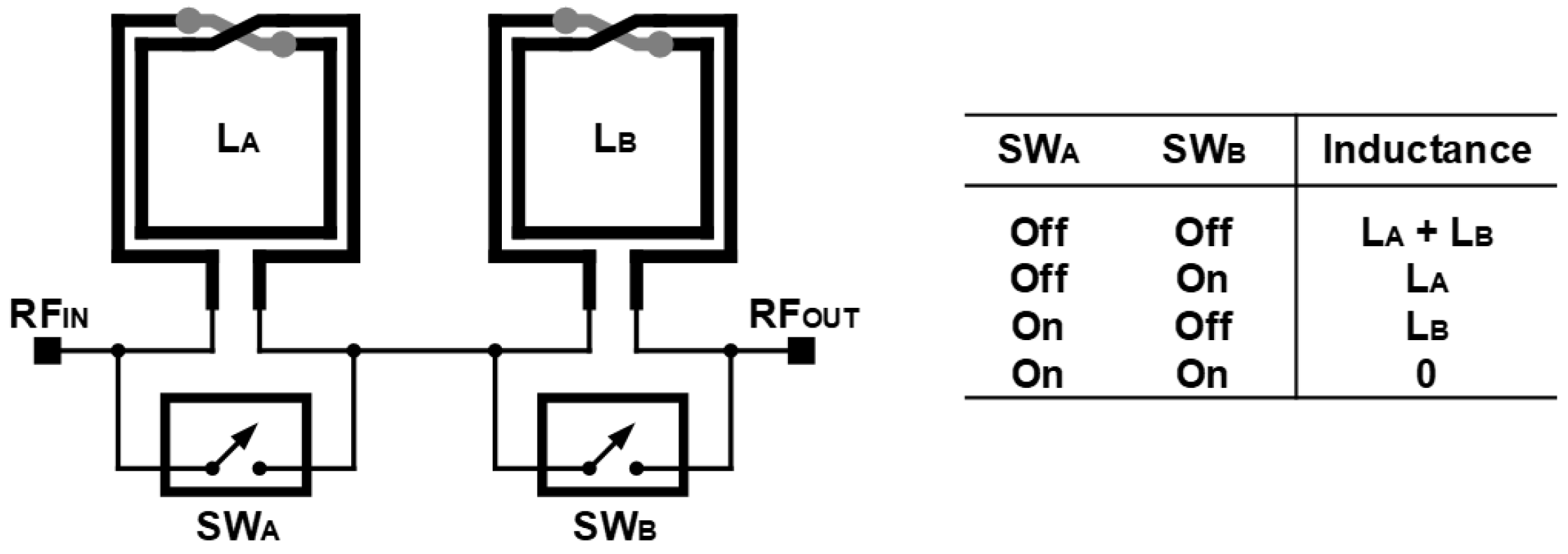
Various approaches to tunable inductors have been investigated to address the need for frequency-agile circuit components in RF and microwave systems. One commonly reported architecture is illustrated in Figure 2, where two inductors, LA and LB, are connected in series, and each inductor is shunted by a switch (SWA, SWB). The effective inductance between the RF input and output ports can be adjusted among 0, LA, LB, or LA + LB, depending on the switching configuration.
This architecture enables discrete, digitally selectable inductance values, which can be advantageous for applications requiring programmable frequency responses. However, several limitations have been identified in practical implementations. First, the use of multiple discrete inductors can result in significant area overhead. Since inductors are inherently bulky components, their integration within compact RF integrated circuit (RFIC) layouts poses challenges for miniaturization and system-level integration.
Second, the performance of tunable inductors is influenced by the characteristics of the switching elements, which are typically implemented using transistor-based devices. As depicted in Figure 3, when a switch is turned on, the associated on-resistance introduces insertion loss, degrading the signal integrity. While increasing the transistor size can reduce this on-resistance, it concurrently increases the parasitic capacitance in the OFF state.
This parasitic capacitance, shown in Figure 4, can form a parallel resonant path with the inductor, even when the switch is OFF, thereby affecting the overall frequency response. In particular, the presence of this unintended resonance can lead to distortion near the parasitic resonance frequency. As the parasitic capacitance increases, the resonant frequency shifts downward, further narrowing the usable frequency range and complicating circuit design.
In summary, while conventional tunable inductor topologies provide functional benefits such as digitally controlled inductance tuning, they are often constrained by trade-offs involving layout area, signal degradation due to switching losses, and resonance-induced distortions caused by parasitic elements. These observations suggest that further exploration of alternative tunable inductor configurations may be beneficial, particularly those that can offer compact implementation, low-loss operation, and minimal parasitic interference.

3. Review of Coupled-Line Tunable Inductor Structures

This section reviews tunable inductor structures based on coupled-line configurations, starting with a discussion of the fundamental operating principles of conventional inductor designs and followed by an examination of implementations involving coupled lines.

3.1. Operating Principle of the Coupled-Line Tunable Inductor

Figure 5a illustrates a conventional line inductor structure. In this case, when a current iL passes through the inductor, no mutual inductive interaction occurs between adjacent metal transmission lines. Thus, the total inductance LL,1 is determined solely by the self-inductance LS of the conductor. In contrast, Figure 5b shows a configuration in which mutual inductance is induced by magnetic coupling between adjacent metal lines. In this case, it is assumed that the two line inductors from Figure 5a, each having a self-inductance LS, are ideally placed adjacent to each other. When current iL flows, an equal and co-directional current is induced in a nearby conductor, generating a positive mutual inductance LM. As a result, the total inductance becomes LL,2 = 2LS + 2LM, exceeding the value of the non-coupled structure. Such configurations often use spiral inductors to realize co-directional current flow.
Based on this concept, Figure 6 presents a configuration intended to reduce inductance through magnetic coupling. In Figure 6a, a coupled line is located adjacent to a conventional line inductor, while being electrically open in the DC sense. Under ideal lossless conditions, an induced current iCL with equal magnitude but opposite direction to iL flows in the coupled line, producing negative mutual inductance—LM,CL. This reduces the total inductance to LT,1 = LL,1 − LM,CL.
Figure 6b extends this principle to spiral inductors, placing a coupled line near the inductor structure. This configuration operates under similar principles, allowing the total inductance to be tuned to LT,2 = LL,2 − LM,CL. These observations suggest that the presence and coupling of a coupled line can influence the inductance value, implying potential utility for inductance tuning. In practice, the mutual inductance LM,CL differs between Figure 6a and b due to their structural and coupling differences.

3.2. Examination of Coupled-Line Tunable Inductor Designs

Considering the effect of coupled lines on total inductance, various designs have incorporated switches within the coupled-line loop to control the induced current iCL, thereby enabling dynamic adjustment of mutual inductance. Figure 7 illustrates this approach.
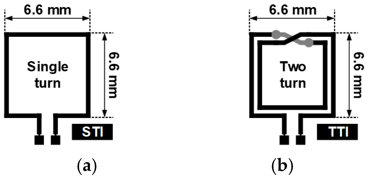
When the switch (SW) is OFF, the current path for iCL is interrupted, preventing the formation of mutual inductance, and the total inductance remains at LL. When the switch is ON, an opposite-direction current iCL is induced by iL in the coupled line, generating negative mutual inductance—LM,CL—and reducing the total inductance to LT = LL − LM,CL. This switching mechanism offers a means for inductance modulation. Spiral inductors with varying turn counts have been utilized as cores in such designs. Figure 8 shows single-turn and two-turn spiral inductor cores with dimensions of 6.6 × 6.6 mm2.
Figure 9 presents coupled-line tunable inductors with two different core configurations. In Figure 9a, a single-turn spiral inductor is implemented with an inner-coupled-line configuration (IC-STI), where the coupled lines are placed inside the core and controlled by a switch to dynamically modulate the mutual inductance. Figure 9b shows a two-turn spiral inductor with an inner-coupled-line configuration (IC-TTI).
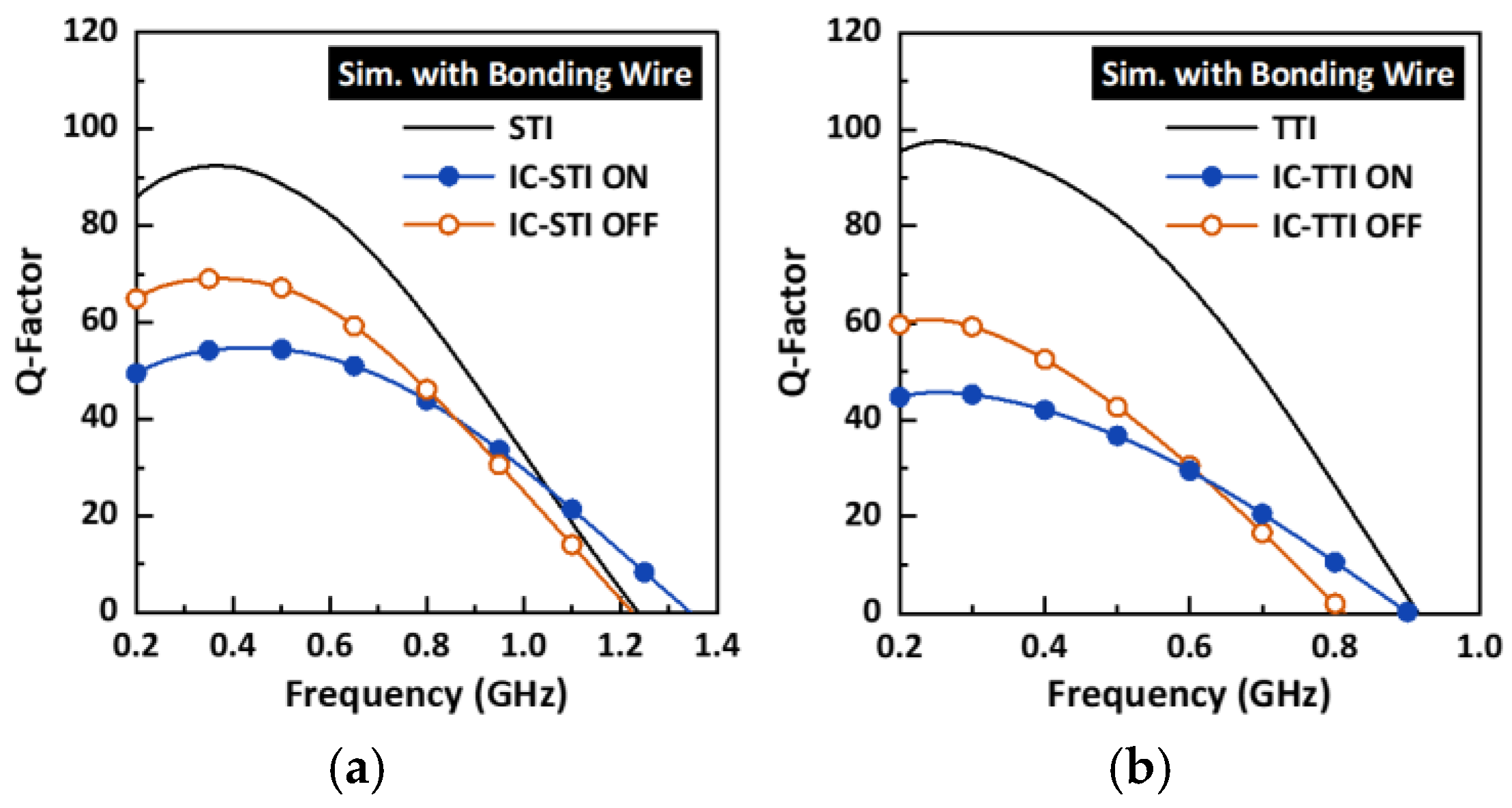
The metal trace widths of both the spiral inductors and coupled lines in these designs are set to 0.5 mm with conductor spacing of 0.1 mm, as shown in Figure 9. Electromagnetic (EM) simulations were performed for the two core configurations presented in Figure 9, namely the IC-STI and the IC-TTI. The simulation results are summarized in Figure 10 and Figure 11. In the ON state of the switch, it was assumed that the two terminals of the switch were connected by an ideal bonding wire.
Figure 10 presents the simulated inductance variation as a function of frequency. For both IC-STI and IC-TTI, turning the switch ON enables the formation of a counter-directional induced current through the coupled lines, which generates negative mutual inductance and consequently reduces the effective inductance.
Figure 11 illustrates the corresponding Q-factor characteristics. In both structures, the reduction in inductance under the ON state results in an upward shift in the self-resonant frequency (SRF). However, the Q-factor gradually decreases with increasing frequency, and its value in the ON state is generally lower than that in the OFF state. This degradation is attributed to additional loss mechanisms and parasitic effects introduced by the coupled-line path.
These simulation results demonstrate that the proposed structures provide tunability not only in inductance magnitude but also in frequency response characteristics, indicating their potential applicability to reconfigurable RF systems.
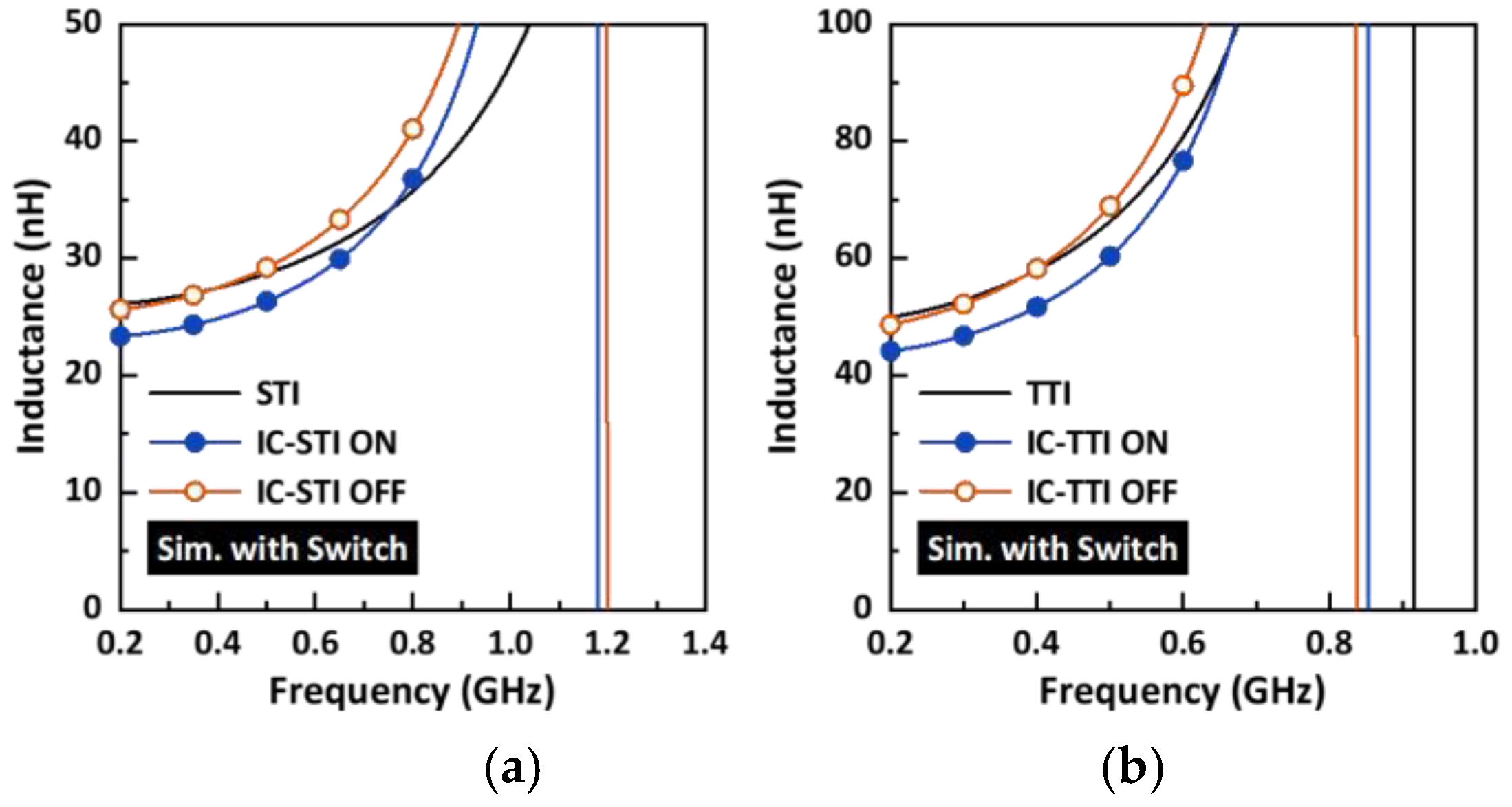
Figure 12 and Figure 13 show the EM simulation results for the IC-STI and IC-TTI structures when the switch is modeled using the PSemi PE4259-63 device (San Diego, CA, USA) to more closely emulate real-world operation.
In the ON state, the modeled switch provides an electrical connection across the coupled line, enabling mutual coupling and resulting in a reduction in the total inductance, as shown in Figure 12. This inductance reduction is accompanied by a corresponding upward shift in the SRF. A quantitative comparison indicates that, at 0.4 GHz, the inductance of the IC-STI decreases by approximately 9.6% when the switch is in the ON compared to the OFF state, while the IC-TTI shows a reduction of about 11.3% under the same condition.
Similarly, the Q-factor characteristics in Figure 13 show a reduction of approximately 52.1% for the IC-STI and 62.3% for the IC-TTI at 0.4 GHz when switching from OFF to ON. Although the ON state generally yields lower Q-factors, both configurations retain significant tunability and offer flexible frequency-response characteristics suitable for reconfigurable RF applications.

4. Design Results of Coupled-Line Tunable Inductors

The inductor core structures and coupled-line tunable inductors shown in Figure 9 were fabricated as prototypes using a PCB process. Two switching implementations were evaluated: using bonding wires to control the coupled-line switching, and using the PSemi PE4259-63 switch device to more closely emulate practical circuit conditions. Although these prototypes were implemented on a PCB for the experimental verification of the coupled-line inductor concept, the underlying design principles were considered applicable to IC environments as well.
Figure 14 and Figure 15 present photographs of the fabricated prototypes. The bonding wire implementation in Figure 14 includes an STI, an IC-STI, a TTI, and an IC-TTI.
The PSemi PE4259-63 implementation in Figure 15 uses the same inductor cores, with the switches connected to the coupled lines via backside metal traces on the PCB. The fabricated prototypes were implemented on an FR4 PCB substrate. In this implementation, conductive traces could be formed on both the top and bottom surfaces of the dielectric layer. The PCB used in this work had a thickness of 1.0 mm and a relative permittivity (εr) of 4.6. The conductive traces on the PCB were realized using copper.
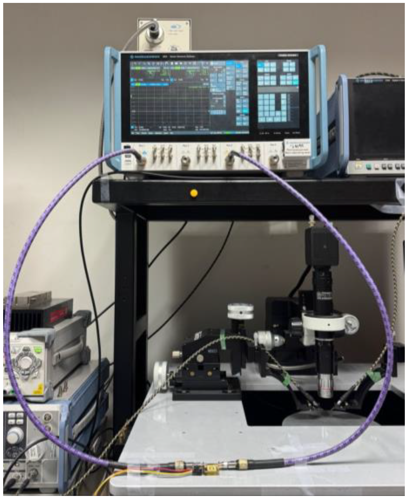
Figure 16 illustrates the measurement setup for the fabricated prototypes. The prototypes were connected to the vector network analyzer (VNA) using RF cables from its two ports to perform the measurements.

4.1. Measurement Results with Bonding Wire Switch Implementation

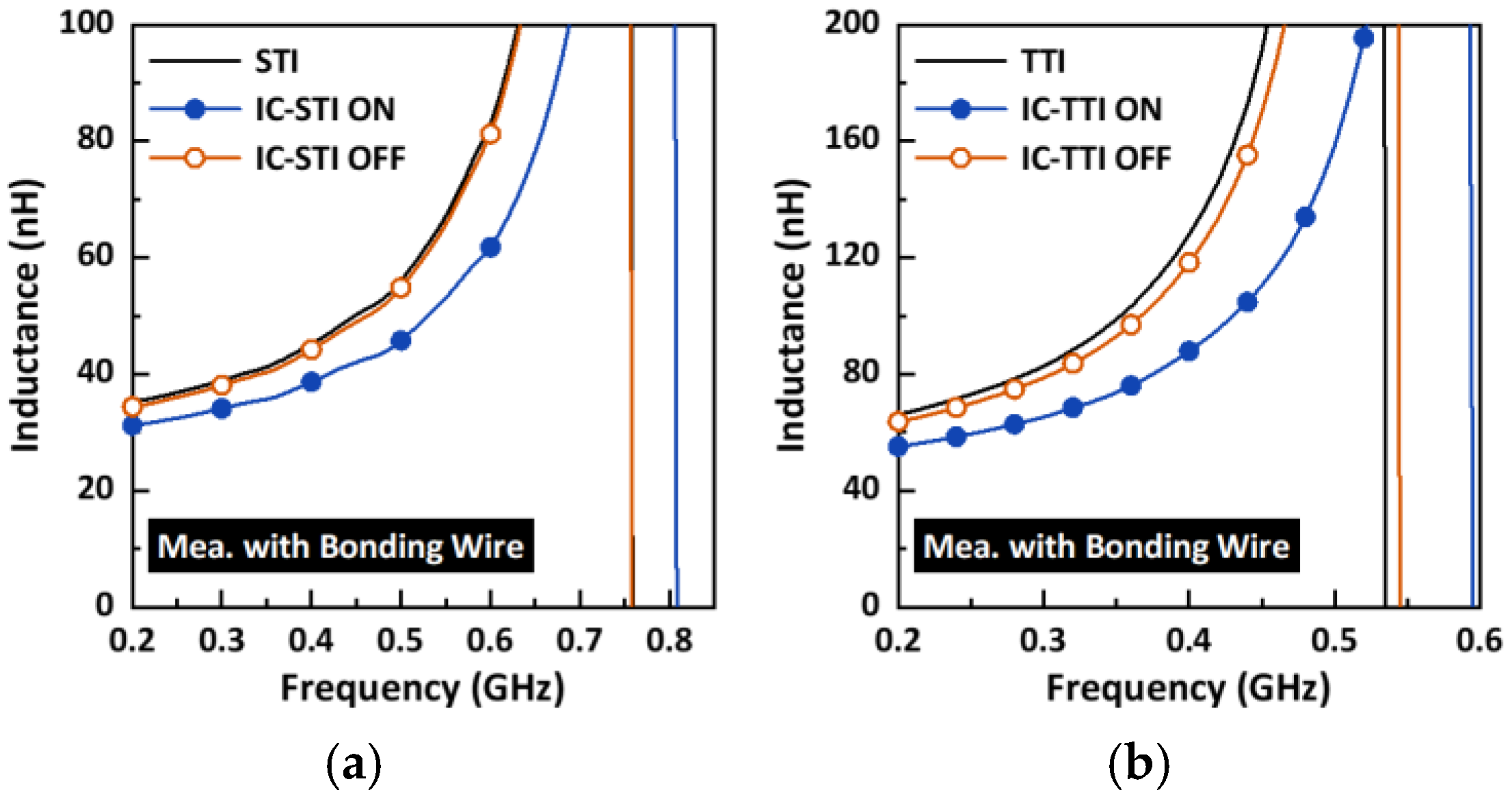
The measured frequency-dependent inductance characteristics for the IC-STI and IC-TTI with bonding wire switches are shown in Figure 17. In the OFF state, the coupled lines are electrically open, preventing current flow and minimizing electromagnetic interaction with the primary inductor. As a result, the inductance values closely match those of the corresponding reference inductors, confirming that the coupled-line structures do not introduce significant parasitic effects without a conduction path.
In the ON state, the coupled lines form a closed-loop current path, enabling mutual magnetic coupling. This induces a counteracting magnetic field that partially cancels the original field, thereby reducing the net inductance and shifting the SRF upward. For both IC-STI and IC-TTI, this inductance reduction trend is consistent with the EM simulation results presented in Figure 10 and Figure 11.
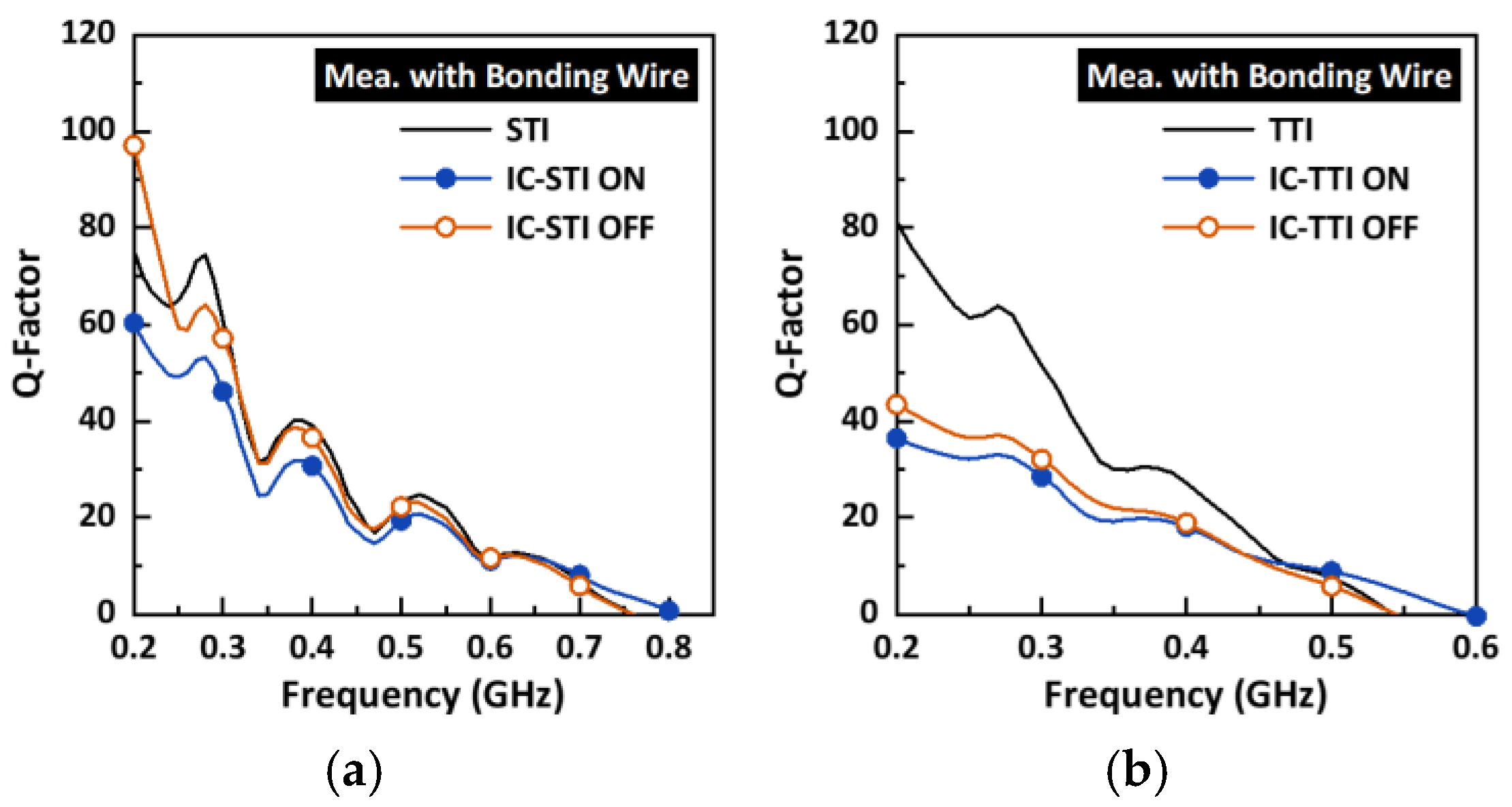
The Q-factor measurements in Figure 18 show a modest reduction in the ON state; however, both configurations retain substantial tuning capability and maintain adaptable frequency responses.

4.2. Measurement Results with Commercial Switch Implementation

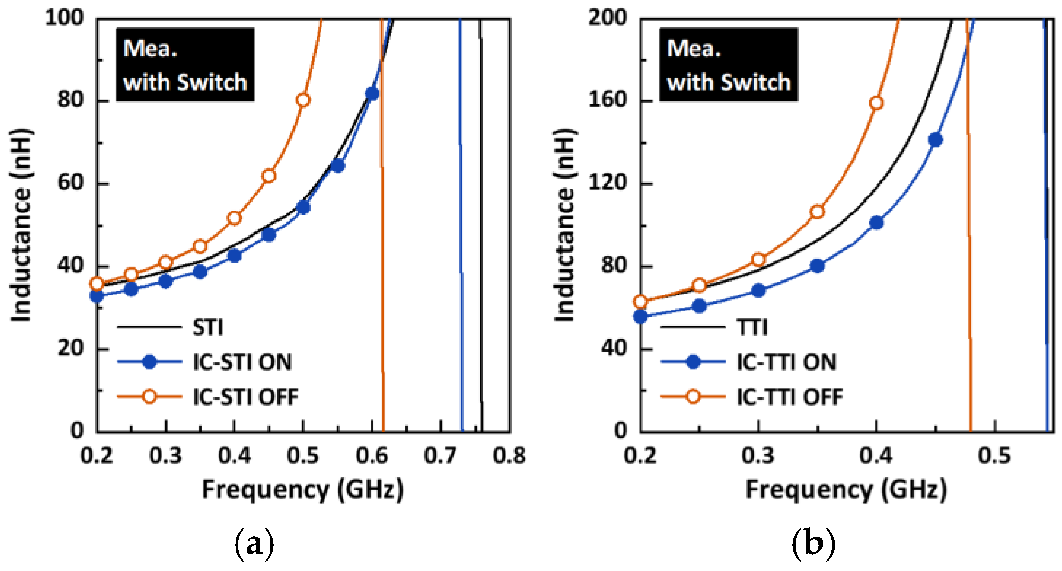
Figure 19 and Figure 20 present the measured results for the IC-STI and IC-TTI with the PSemi PE4259-63 switch device.
The measurement trends are consistent with the bonding wire implementation, confirming the robustness of the proposed concept under more realistic switching conditions. Quantitatively, at 0.4 GHz, the inductance of the IC-STI decreases by approximately 17.6% when the switch is in the ON compared to the OFF state, while the IC-TTI exhibits a reduction of about 36.4% under the same condition, as shown in Figure 19.
Correspondingly, the Q-factor decreases by approximately 19.3% for the IC-STI and 18.2% for the IC-TTI in Figure 20. Despite the slight Q-factor degradation, both structures preserve significant inductance tunability and flexibility in their frequency responses.

5. Conclusions

This study examined the concept of a coupled-line tunable inductor and investigated its characteristics through the design and fabrication of prototype structures. Unlike conventional spiral inductors that provide fixed inductance, the architecture involving switchable coupled lines offered a means to control mutual inductance and thus enabled the modulation of the total inductance. Several configurations based on single-turn and two-turn spiral inductor cores with inner-coupled-line arrangements were fabricated using printed circuit board (PCB) technology, implementing two switching methods: bonding wires and the PSemi PE4259-63 device to emulate practical conditions. These prototypes were analyzed through electromagnetic (EM) simulations and measured with a vector network analyzer (VNA). The experimental results indicate that the inductance can be modulated according to the ON/OFF state of the switch located on the coupled line. Specifically, when the switch is ON, negative mutual inductance is introduced, resulting in a reduction in the total inductance by up to 17.6% for the IC-STI and 36.4% for the IC-TTI at 0.4 GHz, with corresponding Q-factor reductions of 19.3% and 18.2%, respectively. When the switch is OFF, only minor performance degradation is observed, likely due to parasitic effects associated with the coupled line, which appear to be negligible in most cases. The coupled-line tunable inductor concept discussed herein exhibits a relatively simple structure and shows potential for integration in various applications.

Author Contributions

Conceptualization, Y.K.; methodology, Y.K. and J.L.; investigation, Y.K. and S.K.; supervision, C.P.; writing—original draft, Y.K.; review and editing, C.P. All authors have read and agreed to the published version of the manuscript.

Funding

This work was supported in part by the National Research Foundation of Korea (NRF) through the Korea government (MSIT) under Grant NRF-2021R1A2C1013666 and in part by the Institute of Information & communications Technology Planning & Evaluation (IITP) grant funded by the Korea government (MSIT) under Grant RS-2024-00395702.

Data Availability Statement

All the material conducted in this study is mentioned in the article.

Conflicts of Interest

The authors declare no conflicts of interest.

References

  1. Lim, J.; Jeong, G.; Hong, S. A Self-Body-Biasing Network of Vector Sum Phase Shifter for Reduction of Output Capacitance Variation and Supply Current Variation. IEEE Access 2024, 12, 114460–114464. [Google Scholar] [CrossRef]
  2. Jiang, W.; Zhou, Q.; He, J.; Habibi, M.A.; Melnyk, S.; El-Absi, M.; Han, B.; Di Renzo, M.; Schotten, H.D.; Luo, F.-L.; et al. Terahertz Communications and Sensing for 6G and Beyond: A Comprehensive Review. IEEE Commun. Surv. Tutor. 2024, 26, 2326–2381. [Google Scholar] [CrossRef]
  3. Qiu, J.; Pang, J.; Liu, B.; Luo, X.; Wang, Y.; Zhang, Y.; Shirane, A.; Okada, K. A CMOS 24–30-GHz Low-Phase-Variation Variable Gain Amplifier Design for 5G New Radio. IEEE Solid-State Circuits Lett. 2022, 5, 146–149. [Google Scholar] [CrossRef]
  4. Pang, J.; Li, Z.; Kubozoe, R.; Luo, X.; Wu, R.; Wang, Y.; You, D.; Fadila, A.A.; Saengchan, R.; Nakamura, T.; et al. A 28-GHz CMOS Phased-Array Beamformer Utilizing Neutralized Bi-Directional Technique Supporting Dual-Polarized MIMO for 5G NR. IEEE J. Solid-State Circuits 2020, 55, 2371–2386. [Google Scholar] [CrossRef]
  5. Ding, K.; Leenaerts, D.M.W.; Gao, H. A 28/38 GHz Dual-Band Power Amplifier for 5G Communication. IEEE Trans. Microw. Theory Tech. 2022, 70, 4177–4186. [Google Scholar] [CrossRef]
  6. Lee, J.; Paek, J.-S.; Hong, S. Millimeter-Wave Frequency Reconfigurable Dual-Band CMOS Power Amplifier for 5G Communication Radios. IEEE Trans. Microw. Theory Tech. 2022, 70, 801–812. [Google Scholar] [CrossRef]
  7. Bae, B.; Kim, E.; Kim, S.; Han, J. Dual-Band CMOS Low-Noise Amplifier Employing Transformer-Based Band-Switchable Load for 5G NR FR2 Applications. IEEE Microw. Wirel. Technol. Lett. 2023, 33, 319–322. [Google Scholar] [CrossRef]
  8. Lee, J.; Jin, H.; Lee, G.; Sung, E.-T.; Hong, S. A 28/37-GHz Frequency-Reconfigurable Dual-Band 1-Channel Front-End IC for 5G Communication Radios. IEEE Trans. Microw. Theory Tech. 2025, 73, 1882–1895. [Google Scholar] [CrossRef]
  9. Zhang, J.; Chen, J.; Xu, T.; Qin, P.; Yi, X.; Wu, L.; Zhu, H.; Che, W.; Xue, Q. A Compact Dual-mode CMOS Power Amplifier Covering both Sub-6GHz and mm-Wave Bands for 5G NR. In Proceedings of the 2024 IEEE Radio Frequency Integrated Circuits Symposium (RFIC), Washington, DC, USA, 16–18 June 2024; pp. 139–142. [Google Scholar] [CrossRef]
  10. Wen, J.; Wang, R.; Wang, X.; Sun, W.; Sun, L. Multi-Band Millimeter-Wave Circuits for Spectrum Aggregation in B5G Era: A Tutorial. IEEE Trans. Circuits Syst. II Express Briefs 2024, 71, 1656–1662. [Google Scholar] [CrossRef]
  11. Park, P.; Kim, C.S.; Park, M.Y.; Kim, S.D.; Yu, H.K. Variable Inductance Multilayer Inductor with MOSFET Switch Control. IEEE Electron Device Lett. 2004, 25, 144–146. [Google Scholar] [CrossRef]
  12. Lee, S.; Park, J.; Hong, S. A Ka-Band Phase-Compensated Variable-Gain CMOS Low-Noise Amplifier. IEEE Microw. Wirel. Compon. Lett. 2019, 29, 131–133. [Google Scholar] [CrossRef]
  13. Min, D.; Park, C. Ka-Band CMOS Variable-Gain Amplifier Using Capacitive Compensation Technique to Suppress Phase Error. IEEE Trans. Circuits Syst. II Express Briefs 2025, 72, 118–122. [Google Scholar] [CrossRef]
  14. Liu, H.; Boon, C.C.; He, X.; Zhu, X.; Yi, X.; Kong, L.; Heimlich, M.C. A Wideband Analog-Controlled Variable-Gain Amplifier with dB-Linear Characteristic for High-Frequency Applications. IEEE Trans. Microw. Theory Tech. 2016, 64, 533–540. [Google Scholar] [CrossRef]
  15. Fang, M.; Yoshimasu, T. An Ultra-Low-Power Octave-Tuning VCO IC with a Single Analog Voltage-Controlled Novel Varactor. IEEE Trans. Circuits Syst. I Regul. Pap. 2022, 69, 4751–4760. [Google Scholar] [CrossRef]
  16. Lu, K.-C.; Wang, F.-K.; Horng, T.-S. Ultralow Phase Noise and Wideband CMOS VCO Using Symmetrical Body-Bias PMOS Varactors. IEEE Microw. Wirel. Compon. Lett. 2013, 23, 90–92. [Google Scholar] [CrossRef]
  17. Kitagawa, S.; Suzuki, S.; Asada, M. 650-GHz Resonant-Tunneling-Diode VCO with Wide Tuning Range Using Varactor Diode. IEEE Electron Device Lett. 2014, 35, 1215–1217. [Google Scholar] [CrossRef]
  18. Hikmat, O.F.; Mohamed Ali, M.S. RF MEMS Inductors and Their Applications—A Review. J. Microelectromech. Syst. 2017, 26, 17–44. [Google Scholar] [CrossRef]
  19. Park, C. Experimental Investigation of Differential Line Inductor for RF Circuits with Differential Structure. J. Inf. Commun. Converg. Eng. 2011, 9, 11–15. [Google Scholar] [CrossRef]
  20. Guo, L.; Yu, M.; Chen, Z.; He, H.; Zhang, Y. High Q Multilayer Spiral Inductor on Silicon Chip for 5–6 GHz. IEEE Electron Device Lett. 2002, 23, 470–472. [Google Scholar] [CrossRef]
  21. Rais-Zadeh, M.; Kohl, P.A.; Ayazi, F. MEMS Switched Tunable Inductors. J. Microelectromech. Syst. 2008, 17, 78–84. [Google Scholar] [CrossRef]
  22. Feng, J.; Lu, L.; Chen, X.; Sun, Y.; Wu, X.; Fan, X.; Li, L. A 60-GHz Variable-Gain Power Amplifier with a Switchable Inductor for TDD Systems. IEEE Microw. Wirel. Technol. Lett. 2024, 34, 512–515. [Google Scholar] [CrossRef]
Figure 1. Tunable passive components and their typical implementation methods: (a) variable resistor and (b) varactor.
Electronics 14 03228 g001
Figure 2. An example of a conventional inductance tuning method using multiple inductors and switches, and its inductance variation according to the switching states.
Electronics 14 03228 g002
Figure 3. Parasitic components depending on the switch state: (a) switch ON state and (b) switch OFF state.
Electronics 14 03228 g003
Figure 4. Equivalent circuits of an inductor–switch parallel structure depending on the switch state: (a) switch ON state and (b) switch OFF state.
Electronics 14 03228 g004
Figure 5. Conceptual diagrams of conventional inductance generation methods: (a) line inductor without mutual inductance and (b) two line inductors with mutual inductance caused by interaction between adjacent metal lines.
Electronics 14 03228 g005
Figure 6. Conceptual diagrams of inductance variation in conventional methods with closely coupled metal lines: (a) line inductor with mutual inductance and (b) two line inductors with mutual inductance caused by interaction between adjacent metal lines.
Electronics 14 03228 g006
Figure 7. Coupled-line tunable inductor with ON–OFF functionality using switch: (a) conceptual circuit diagram and (b) inductance variation according to the switch ON/OFF states.
Electronics 14 03228 g007
Figure 8. Inductor cores for implementing coupled-line tunable inductors: (a) single-turn spiral inductor and (b) two-turn spiral inductor.
Electronics 14 03228 g008
Figure 9. Coupled-line tunable inductors with different core configurations: (a) inner-coupled single-turn inductor (IC-STI) and (b) inner-coupled two-turn inductor (IC-TTI).
Electronics 14 03228 g009
Figure 10. Simulated inductance characteristics of (a) IC-STI and (b) IC-TTI, with the switch implemented using an ideal bonding wire.
Electronics 14 03228 g010
Figure 11. Simulated Q-factor characteristics of (a) IC-STI and (b) IC-TTI, with the switch implemented using an ideal bonding wire.
Electronics 14 03228 g011
Figure 12. Simulated inductance of coupled-line tunable inductors using (a) IC-STI and (b) IC-TTI cores, with the switch modeled after the PSemi PE4259-63 device.
Electronics 14 03228 g012
Figure 13. Simulated Q-factor of coupled-line tunable inductors using (a) IC-STI and (b) IC-TTI cores, with the switch modeled after the PSemi PE4259-63 device.
Electronics 14 03228 g013
Figure 14. PCB prototypes with bonding wire switches: (a) STI, (b) IC-STI, (c) TTI, and (d) IC-TTI.
Electronics 14 03228 g014
Figure 15. PCB prototypes with PSemi PE4259-63 switch device connected to coupled lines via backside metal traces: (a) top side of IC-STI, (b) bottom side of IC-STI, (c) top side of IC-TTI, and (d) bottom side of IC-TTI.
Electronics 14 03228 g015
Figure 16. Measurement setup using a VNA with two ports connected to the prototypes via RF cables.
Electronics 14 03228 g016
Figure 17. Measured inductance characteristics of (a) IC-STI and (b) IC-TTI with bonding wire switch.
Electronics 14 03228 g017
Figure 18. Measured Q-factor characteristics of (a) IC-STI and (b) IC-TTI with bonding wire switch.
Electronics 14 03228 g018
Figure 19. Measured inductance characteristics of (a) IC-STI and (b) IC-TTI with PSemi PE4259-63 switch device.
Electronics 14 03228 g019
Figure 20. Measured Q-factor characteristics of (a) IC-STI and (b) IC-TTI with PSemi PE4259-63 switch device.
Electronics 14 03228 g020
Disclaimer/Publisher’s Note: The statements, opinions and data contained in all publications are solely those of the individual author(s) and contributor(s) and not of MDPI and/or the editor(s). MDPI and/or the editor(s) disclaim responsibility for any injury to people or property resulting from any ideas, methods, instructions or products referred to in the content.