Article

Suppression of Cohesive Cracking Mode Based on Anisotropic Porosity in Sintered Silver Die Attach Encapsulated by Epoxy Molding Compounds

ROHM Co., Ltd., Kyoto 615-8585, Japan
*
Author to whom correspondence should be addressed.
Electronics 2025, 14(16), 3227; https://doi.org/10.3390/electronics14163227
Submission received: 30 June 2025 / Revised: 12 August 2025 / Accepted: 13 August 2025 / Published: 14 August 2025

Abstract

This paper investigates the suppression of the cohesive cracking mode (CCM) in the sintered silver (s-Ag) die layer by intentionally introducing anisotropic porosity through two press sintering methods. Full press (FP) and local press (LP) bonding represent the s-Ag formed by pressing the die-attached assemblies (DAAs) on either the entire top surface or only on the silicon carbide (SiC) top surface, respectively. The fabricated DAAs were encapsulated with epoxy molding compounds. Degradation was evaluated using a nine-point bending test (NBT) under cyclic force between 0 and 270 N with a triangle waveform for 3 min per cycle at 150 °C. Scanning tomography images after 500 NBT cycles showed that the LP reduced the inner degradation ratio by up to 21.1% compared to the FP. Cross-sectional scanning electron microscopy revealed that the FP progressed cracking in the s-Ag die layer, whereas the LP showed no evidence of cracking. A finite element analysis revealed that in the FP, the accumulated plastic strain (APS) was concentrated in the s-Ag layer within the inner SiC chip. In contrast, the APS of the LP was preferentially concentrated outside the SiC chip. This preferential localization of damage outside the chip presents a promising approach for enhancing the reliability of packaging products.

1. Introduction

Packaging (PKG) for power electronics involves bonding multiple materials together. Typically, semiconductor dies are bonded to directly bonded copper substrates or active metal brazing substrates. These die-attached assemblies (DAAs) are then encapsulated using epoxy molding compounds (EMCs) [1]. Recently, power conversion systems have required PKG with a higher power density [2]. Power devices based on so-called-wide bandgap (WBG) materials are considered to be the key to meeting this goal [3,4]. However, WBG materials also introduce new technological challenges. A high power density inherently reduces the available pathways for heat dissipation in power conversion systems, necessitating the use of high thermal conductivity materials. To meet this requirement, sintered metal bonding techniques, such as sintered silver (s-Ag), have been explored as promising solutions because of s-Ag’s relatively higher thermal conductivity than conventional soldering materials [5,6]. However, the porosity in s-Ag limits its industrial application because it leads to low thermal conductivity. Therefore, pressurized s-Ag has gained attention as an effective die attach material because applying pressure during sintering significantly reduces porosity [7,8,9,10]. Additionally, meeting the AQG324 qualification standards has become essential for evaluating PKG reliability [11]. The thermal shock test (TST), which subjects samples to alternating high and low ambient temperatures for specific durations, is widely used to assess PKG reliability. It has been widely adopted to assess the reliability of PKG. Due to the different coefficients of the thermal expansion (CTE) among the various components, the TST induces thermal and mechanical stress, often leading to failure [12]. Two primary failure modes are often observed during the TST: a cohesive cracking mode (CCM) in the die layer [13,14,15] and an interface delamination mode (IDM) at the metal/metal or EMC/metal [16,17]. To simplify the TST assessment, we developed a nine-point bending cyclic test (NBT), which can provide the similar out-of-plane deformation observed during the TST by applying a force variation at a specific temperature [18]. We previously demonstrated that the NBT at 150 °C reproduced the s-Ag CCM observed in the TST conducted over a temperature range from 40 °C to 150 °C. The advantage of the NBT lies in its isothermal environment and precise control of the mechanical motion, making it well-suited for identifying the root cause of the CCM.
Cracking that develops horizontally beneath the semiconductor chips is a critical failure mode because it significantly increases the thermal resistance of the PKG (Rth). Rth is defined as the temperature difference between the highest temperature at the chip and the ambient temperature, divided by the power loss at the chip [19,20,21]. The Rth increase ratio (rth) is defined as the relative increase in the Rth after reliability tests, calculated by dividing the change in Rth by the initial Rth. This increase is primarily caused by degradation within the chip, which hinders the thermal pathway from the chip to the lower-side material. In general, the lifetime of a product is defined as the point at which rth reaches 20% [11]. As an inspection methodology for the existence of cracking, scanning acoustic tomography (SAT) has been commonly used for nondestructive inspections. A high acoustic reflection intensity in the die layer corresponds to the existence of air inside, signifying degradation due to horizontal cracking. There is a positive correlation between the product lifetime and the degradation area ratio in the die layer as measured by SAT; when the degradation exceeds 20%, the product is considered to have reached its lifetime limit [22,23]. Therefore, a key design objective is to suppress the cracking area in the die layer during the reliability tests. Among the CCM and IDM, the CCM is more manageable from a design perspective. This is because the CCM progresses slowly and steadily over time, whereas the IDM tends to propagate dynamically and unpredictably [24]. The following section will focus on reviewing the design strategies for mitigating the CCM.
The level of damage in the CCM of the s-Ag layer was assessed by the accumulated plastic strain (APS) per cycle, which was calculated by a finite element analysis (FEA), considering the experimental conditions [25,26,27,28]. The APS of the s-Ag especially increases at high temperatures, when the temperatures exceed the point at which the tensile mechanical property of s-Ag changes from elastic to plastic, which usually occurs at approximately 100 °C [29,30,31]. This transition temperature is indexed as “HT” in this section. From this viewpoint, lowering the maximum temperature is favorable for suppressing the CCM [32,33]; however, this is not practical. If high maximum temperatures are required, die material modification in the DAA is the primary approach. Three aspects for increasing the lifetime in the s-Ag die layer during the TST are introduced.
The first approach involves modifying the porosity and elemental composition of the s-Ag layer. To increase the plasticity range at high temperatures exceeding HT, a less porous structure is preferred. This can be effectively achieved by increasing the applied pressure during the hot sintering process [34,35,36,37,38,39]. As a result, less porous s-Ag positively decreases die degradation by increasing the durability of the APS during the TST [31,32]. Additionally, adding another element, such as a diamond, boron nitride, or copper oxide, to s-Ag positively enhances the material strength at exceeding HT by restricting the Ag grain motion during TSTs [39,40,41,42,43]. However, this strengthening phenomenon simultaneously sacrifices the s-Ag plasticity at high temperatures, which has still not been demonstrated in the lifetime enhancement in the TST [39,42].
The second approach concerns the thickness of the s-Ag layer. Among the various PKG materials, the CTE gap between the semiconductor and substrate is typically the highest. Increasing the thickness of the s-Ag die layer reduces the APS per cycle during the TST, as shown by the FEA [43,44]. For instance, the degradation in a 100 µm thick s-Ag layer after 1000 TST cycles was reduced to one-third of that in a 50 µm thick layer under the same TST conditions [32]. Furthermore, increasing the die layer and the filet height of the s-Ag also contributes to reducing the concentration of the APS, which is located at the corner of the chip edge, as previously discussed in solder DAAs [45,46].
The third approach focuses on controlling the stress gradient within the s-Ag layer. As previously noted, the durability of s-Ag is highly sensitive to its porosity distribution. When the porosity is inhomogeneous in the s-Ag layer, the cracking behavior during the TST can change. For the horizontal porosity distribution of the s-Ag die layer, DAAs with active metal brazing substrates and soft copper unintentionally resulted in a hill valley surface configuration. These irregularities led to the formation of multiple diagonal cracks in the s-Ag layer after 2400 TST cycles [47]. The expectation is that the total horizontal crack length will be suppressed by replacing a generation of diagonal cracks; however, this crack change has not yet been demonstrated to improve the lifetime of the TST. For the vertical porosity distribution of the s-Ag die layer, Zhao et al. [48] found that pore segregation is found beneath the SiC chip after thermal storage at 350 °C for 800 h. They took a more deliberate approach by creating a vertical pore gradient, stacking two s-Ag layers with different sintering temperatures and applying stress profiles. This pore gradient in the die layer effectively reduces the thermomechanical stress, as confirmed by the FEA simulations. The degradation ratio after the TST in this gradient s-Ag layer was 5% lower than that in DAAs with homogeneous porosity [49]. However, this method increases the risk that the Rth increases due to the worsening of the thermal conductivity of the larger porosity in the s-Ag layer [7,8,9,10]. If the porosity level remains within the die layer but maintains the microstructure, it is possible to achieve reliable PKG with a low Rth.
In this study, we attempted to suppress the CCM by intentionally creating anisotropic porosity in the s-Ag layer in the horizontal direction via two pressings. Both pressings maintain a small porosity of s-Ag within the die layer. The outer side of the chip’s s-Ag porosity is regulated by the applied pressure. The remainder of this paper is organized as follows. Section 2 describes the assessment flow of the PKG reliability and clarifies how we intentionally created the anisotropic porosity in the s-Ag layer. Section 3 presents the degradation results of the PKG after the NBT as a function of NBT cycles. The degradation portion after the NBT was inspected by SAT. The failure mode was investigated by backscattering electron (BSE) images of the cross-sectional scanning electron microscopy (SEM). In Section 4, the FEA was used to discuss the APS distribution and failure mode correlations. Finally, Section 5 presents the conclusion.

2. Materials and Methods

Figure 1 shows the experimental schematic view of this study. First, a commercial Ag paste was screen-printed on the metal substrate. The 64Ti (Ti 90%, Al 6%, and V 4% in weight) with Ag sputtering was adopted for the metal substrates. The 64Ti prevents plastic deformation during NBT to maintain test controllability. Ag sputtering improves the adhesivity with the s-Ag die layer. A 0.2 mm thick stainless steel metal plate with a 9 mm squared hole was used as the stencil mask.
The printed Ag was then dried at 140 °C for 90 min in air. After drying, a 4.8 mm square SiC chip with a thickness of 0.35 mm was mounted on the center of the dried Ag layer. The external uniaxial press was then applied by uniaxial motion while supplying heat. As shown in the top left schematic view of Figure 1, the press region was adjusted by changing the carbon sheet size. “FP” and “LP” refer to the s-Ag die layer formed by pressing the entire top surface of a DAA or the SiC chip of a DAA, respectively. In this study, the carbon sheet size of FP and LP was 20 + 0.2 mm and 4.8 + 0.2 mm square, respectively. The carbon sheets are manually placed at the center of the DAAs. The applied force for FP and LP was regulated to 24 kN and 1.38 kN to provide the 60 MPa pressure on the pressed area. The thickness of the s-Ag layer at the pressed area was set to 50 μm. SEM bird-view images show the porous structure of the s-Ag layer between the FP and LP, which is located outside the SiC chip. For the FP, outside s-Ag, almost all surfaces appear smooth in the overall image, except for the area surrounding the SiC chip edge. Since the applied stress direction is uniaxial, in the edge portion surrounding the SiC chip it was difficult to supply enough pressure. To prevent this occurrence, cold isostatic press sintering is a promising approach for applying hydrostatic pressure with a sufficient press at the edge region [50]. For a more detailed view of the pressed area, the crystal is aggregated to form a bulk sputtered Ag as-deposited surface [51]. Note that a tiny nanoporous material was found at the grain boundary.
For the LP, the difference from the FP is twofold. As observed from the overall SEM image, a groove with approximately 20 μm width is found surrounding the SiC chip. When the SiC chip was locally pressed, it sank to actively create space between the SiC chip and outer s-Ag layer. The outside overall s-Ag layer in the LP is more rugged than the surface in the FP outside the s-Ag layer. The enlarged SEM view shows that the s-Ag has a microsized porous structure, resulting from insufficient sintering under no pressure. The average grain diameter of non-pressed s-Ag was approximately 1.8 μm, which was approximately three times larger than that of the pressed s-Ag observed outside the s-Ag layer in FP, due to insufficient sintering. Consequently, FP and LP successfully created a porous structure distinction on the outside of the SiC chip in the DAAs. Although it is not presented in this paper, the porous control method has scalability because the porous state can be attained by only changing the cushion size in the uniaxial press tester, which is manufactured by companies like Boschman Technologies [52] and Webber GmbH [53].
After fabricating the DAA, the EMC powder was thermo-compressed in the molding machine. Then, as illustrated in step 3 of Figure 1, a UV laser was used to process the DAA so that the EMC and s-Ag die layer were the same size. This encapsulated DAA is the evaluated PKG in this study. The PKG was set between eight support pins and one push pin, which was the same configuration as in our previous studies [18]. The NBT was conducted under a cyclic force between 0 and 270 N with a triangle waveform for 3 min per cycle at 150 °C. The stress level of NBT corresponds to the stress level during TST, changing the temperature from 40 °C to 150 °C [31]. The detailed experimental conditions for each step, including the machine and material information, are presented in Table 1.
SAT was used to evaluate the degradation area of the PKG after 100, 300, and 500 cycles of NBT. BSE images of cross-sectional SEM after NBT were used to assess the failure mode trajectory from initial, 100, and 500 cycles of NBT in the FP and LP PKG. FEA based on the PKG in FP and LP was used to examine the differences in the failure mode between the FP and LP PKG.

3. Results

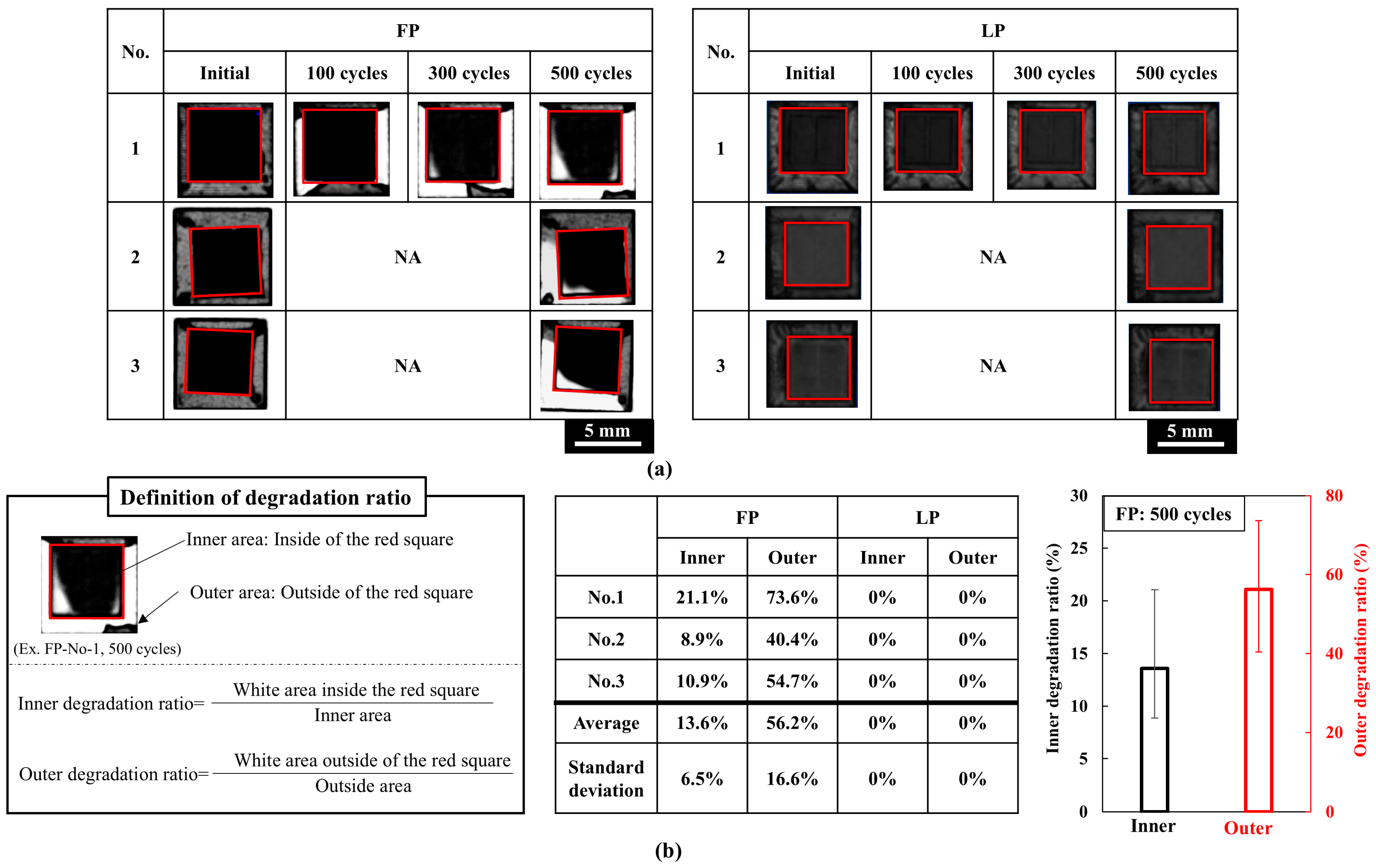
Figure 2a shows the SAT images for the NBT initially and at 100, 300, and 500 cycles of the FP and LP. The number of samples for the NBT was set to three. The SAT images in one sample indexed as No. 1 were examined initially and at 100, 300, and 500 cycles to confirm the degradation progress during the NBT. The SAT images in two samples indexed as No. 2 and 3 were examined initially and at 500 cycles to confirm the divergence of results after 500 cycles of the NBT. All images were taken from the bottom side using an ultrasonic probe at 25 MHz. The color difference represents the difference in the reflective acoustic intensity. The lighter color represents the degradation area, which corresponds to the high reflective intensity caused by the air inside. In contrast, the darker color represents no such air, meaning that no degradation occurred in this area. The red frame represents the die area, which corresponds to the SiC chip area. For FP-No. 1, degradation mainly occurred after 100 cycles of the NBT on both sides of the areas located outside the die area. This degradation area spread to the bottom outside area after 300 cycles. Notably, the degradation can also be found at the bottom left corner within the die area. After 500 cycles, the degradation occurred not only in the outer area but also in the inner die area. The other samples of FP-No. 2 and 3 also showed degradation, as observed in the 500 cycles of FP-No. 1. In contrast, LP-No. 1 always shows a darker color in the images from the initial start to 500 cycles of the NBT. LP-No. 2 and 3 also showed no degradation after 500 cycles of the NBT.
Figure 2b shows the numerical analysis results of the degradation ratio in the inner and outer regions of the SiC chip die area based on the 500-cycle SAT images of the NBT in the FP and LP in Figure 2a. The definition of the degradation ratio is provided in the “Definition of degradation ratio” box in Figure 2b. According to the numerical analysis results in the table, as shown in the middle of Figure 3b, the inner and outer degradation average values at the FP were 13.6% and 54.7%, respectively. In contrast, the LP shows 0% in those values. That is, the FP shows degradation not only on the inner but also on the outer side during the NBT. The standard variation value of the degradation ratio in the FP was 6.5% for the inner region and 16.6% for the outer region. In addition, we showed the bar graph on the right side of Figure 3b to illustrate the full range of the FP data after 500 cycles of the NBT, from the minimum to the maximum value. According to the bar graph results, the inner degradation ratio for the FP after 500 cycles is 13.6 4.7 + 7.5 %. This implies that the LP degradation suppression effect from the FP inner degradation ratio achieves up to 21.1%. This improvement is particularly noteworthy, as it represents a significant enhancement over the previously reported 5% reduction achieved using vertical inhomogeneous porosity distribution techniques [49]. Additionally, the outer degradation ratio in the FP is 56.2 15.8 + 17.4 %.
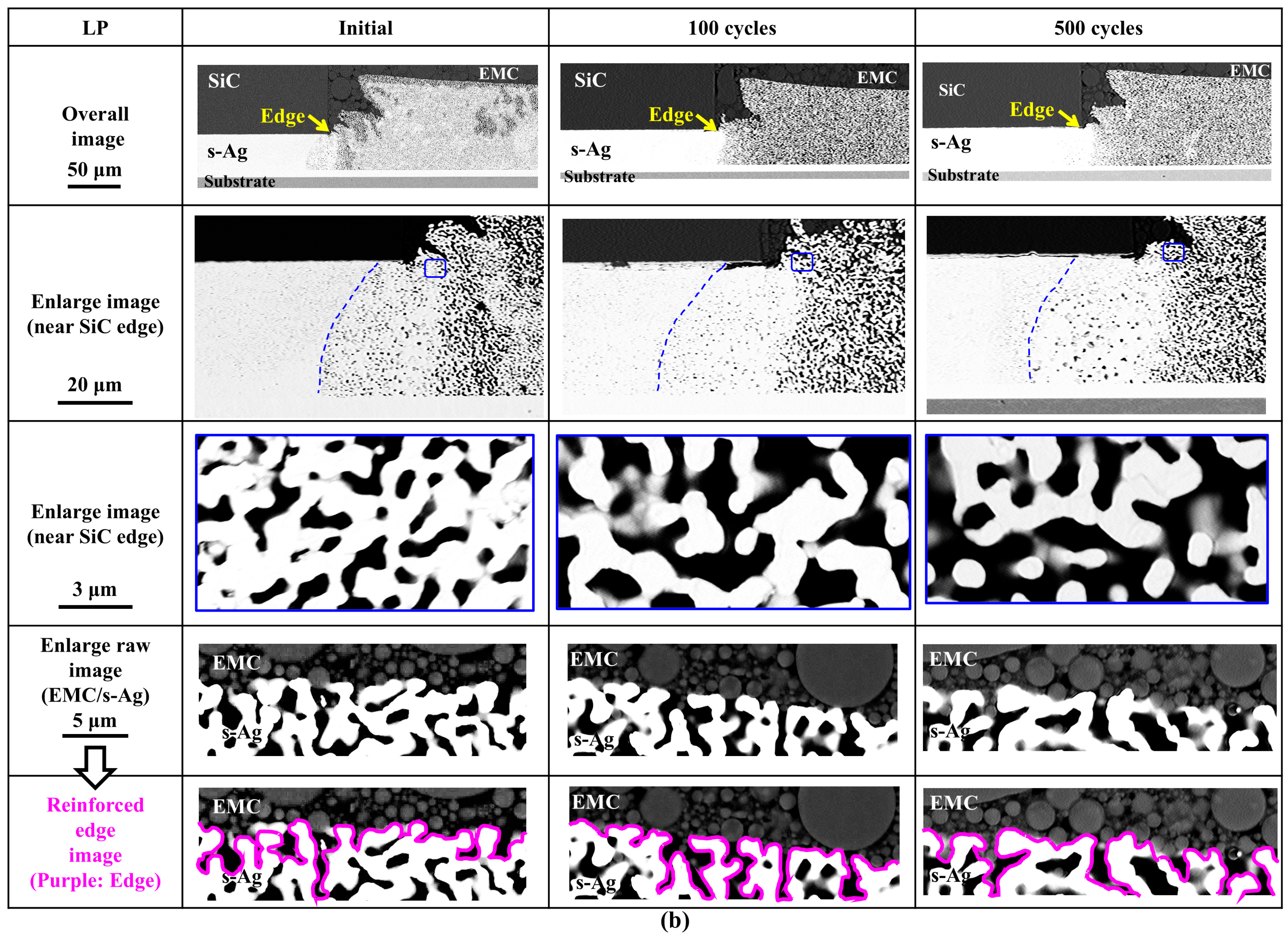
To determine the reason for the degradation difference between the FP and LP during the NBT, a cross-sectional BSE SEM analysis was performed as a function of the NBT cycle. Figure 3a,b show the cross-sectional BSE SEM observation results at the initial stage, 100, and 500 cycles of the NBT for the FP and LP, respectively. Five types of images were captured to elucidate the state of the DAAs in each condition. The top line shows an overall image to understand the shape of the s-Ag layer in the PKG. The second line shows an enlarged image near the SiC edge to illustrate the cracking behavior. The third line shows a local image in the blue square area, as depicted in the second line, to illustrate the s-Ag pore microstructure morphology. The fourth line shows the enlarged image of the EMC/s-Ag to examine the bonding state. The fifth line shows the reinforced edge image to illustrate the interface status.
For the FP at the initial stage of an overall image, the s-Ag layer crawls up at the side wall of the SiC chip, and the s-Ag layer shows a gradual downward slope to the outside. The s-Ag layer shows a homogeneous porous structure both beneath and outside the SiC chip, as observed in the second-line image. The porosity level was approximately 5%. and the pore shape was circular, as observed from the enlarged third-line image. This pore morphology is similar to the previous results of the pressurized s-Ag at a 60 MPa pressure at 300 °C for 10 min [54]. Consequently, we confirmed that the FP successfully achieved the homogeneous porosity in the s-Ag layer at the initial stage. For the EMC/s-Ag, the interface is almost flat, as seen from the fourth- and fifth-line images.
For FP at 100 cycles of NBT, the CCM in the s-Ag die layer is visible, as shown in the first- and second-line images. The inclined crack damage starts from the corner of the SiC chip edge to the s-Ag layer inside. Note that the irregular pore shape is located close to the SiC chip edge, resulting in increased porosity, as observed from the third-line image. The porosity level increases to 12%, which is 2.4 times higher than that at the initial. Additionally, IDM is visible between EMC and s-Ag, as observed from the fourth- and fifth- line images.
For the FP at 500 cycles of the NBT, both failure modes are still visible, as seen during the 100 cycles of the NBT. The primary difference in the CCM between the 100 and 500 cycles of the NBT is the cracking propagation in the s-Ag die layer. With 500 cycles of the NBT, the crack ran along the substrate surface in a horizontal direction, as seen from the second-line image. The porosity continues to increase at 24%, and the pore is located closely, as seen from the third-line image. It is well-known that the s-Ag pore growth is associated with Ag sliding under applied stress at high temperatures [31]. Consequently, this pore growth from the initial state to 500 cycles is related to the stress concentration at the edge of the SiC chips during the NBT. A detailed discussion will be presented in the next section based on the FEA results. The EMC/s-Ag delamination is still found in the fourth- and fifth-line images.
In stark contrast with the LP case, the cross-sectional morphologies show an entirely different tendency from those in the FP. For the initial state, the s-Ag morphology in the LP showed no crawling up along the SiC chip side, as seen in the first-line image. For the SiC chip outside, the thickness of the s-Ag layer is almost the same as that of the SiC die layer up to 50 μm outward from the edge. After that, the thickness is approximately twice that of the SiC die layer. This increased thickness is attributed to a higher porosity in the s-Ag layer at the outside of the SiC chip under the no-pressure condition, as depicted in Figure 1. The s-Ag layer has a distinct structure along the horizontal line, as seen in the second-line image. Dense structures are observed beneath the SiC chip, as seen in the FP porosity at the initial state. In contrast, a higher porous structure is observed outside the SiC chip. It is worth noting that the SiC chip inside the approximately 20 μm width within the blue dashed region shows more porosity than the inside of the SiC chip. The porosity level was 13%. Thus, the proposed LP has a slight pore gradient from the SiC chip inside to the SiC chip outside. In the third-line image, nonuniform microsized pores are randomly located in the blue square, as depicted in the second-line image. The porosity level on the outside was 25%, which originated from a smaller press outside the SiC chip. Additionally, the high porosity produces a rugged EMC/s-Ag interface, as depicted in the forth- and fifth-line image. This rugged interface seems preferable for suppressing delamination during the NBT because an increased interface region increases the toughness [55,56]. After 100 and 500 cycles of the NBT in the cross-sectional BSE images, the morphology remained almost identical to its initial state, with no delamination observed at the EMC/s-Ag and no cracking in the s-Ag layer beneath the SiC chip. The difference from the initial state to 100 and 500 cycles is the microstructure of the s-Ag layer, as shown in the third-line images. For 100 and 500 cycles, the Ag grains are located separately, like the discontinuous cracking from the initial state that has a Ag grain connection.
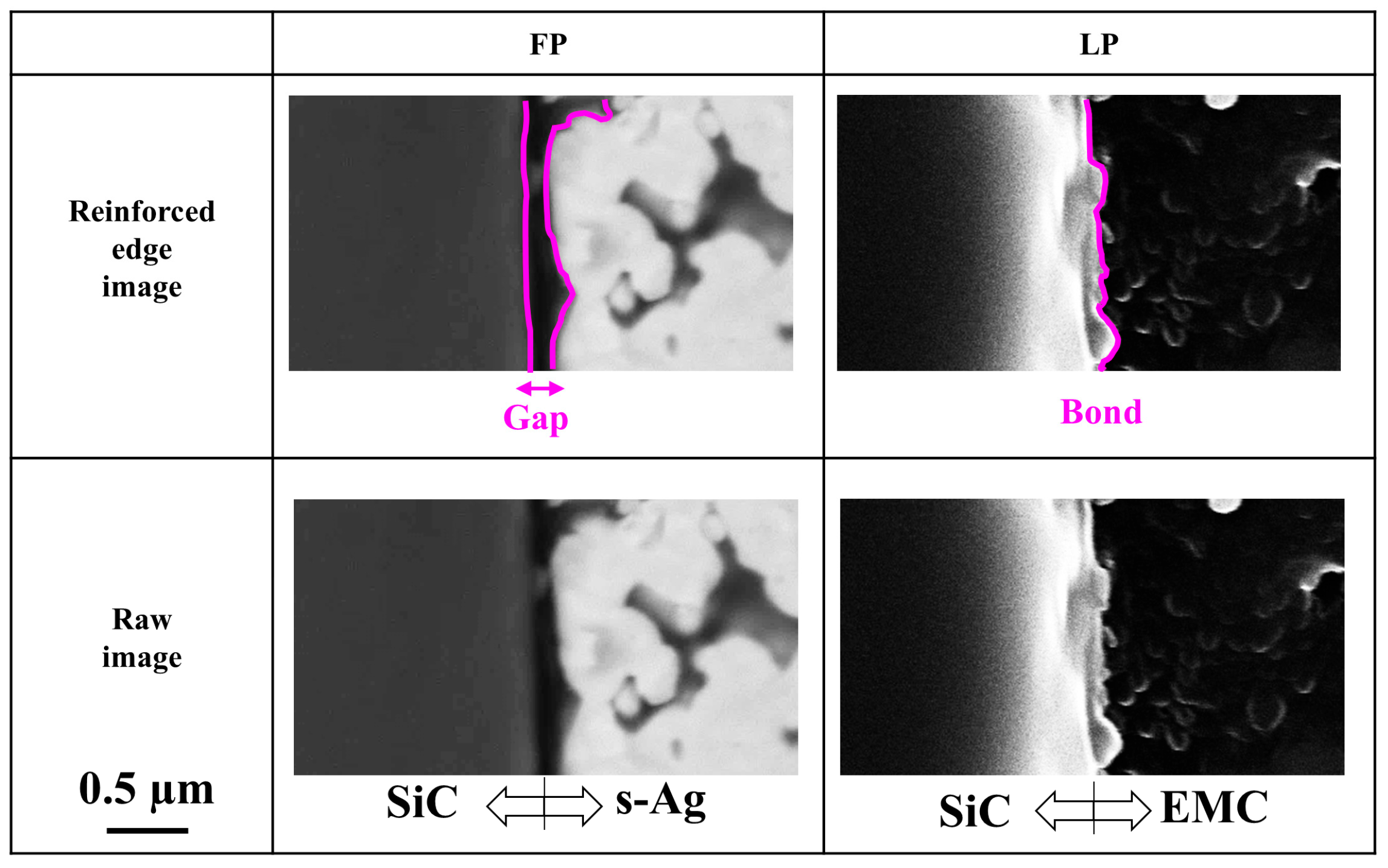
We also investigated the adhesive condition between the SiC chip side wall and the adjacent material after 100 cycles of the NBT in the FP and LP using local cross-sectional SEM observations to accurately reflect the model configuration in the FEA, as will be presented in the next section. The choice of 100 cycles for this observation corresponds to the start cycle of the fracture mode difference between the FP and LP during the NBT. Figure 4 shows an enlarged view around the side of the SiC chip for the FP and LP after 100 cycles of the NBT, along with the reinforced edge images. For the FP sample, a visible gap exists between the SiC and s-Ag. The s-Ag also exhibited irregular pore shapes similar to those observed in the pressureless s-Ag layer that exists outside of the SiC chip of the LP in Figure 3b. This gap is attributed to the insufficient sintering of the s-Ag, which is likely caused by the limitations of uniaxial pressing. In contrast, the LP sample shows complete adhesion between the EMC and the SiC chip without any gaps in the LP. Therefore, we conclude that the FP after 100 cycles of the NBT is a discontinuous structure with SiC side wall/s-Ag and EMC/s-Ag, whereas the LP after 100 cycles of the NBT still maintains a perfect continuous structure.
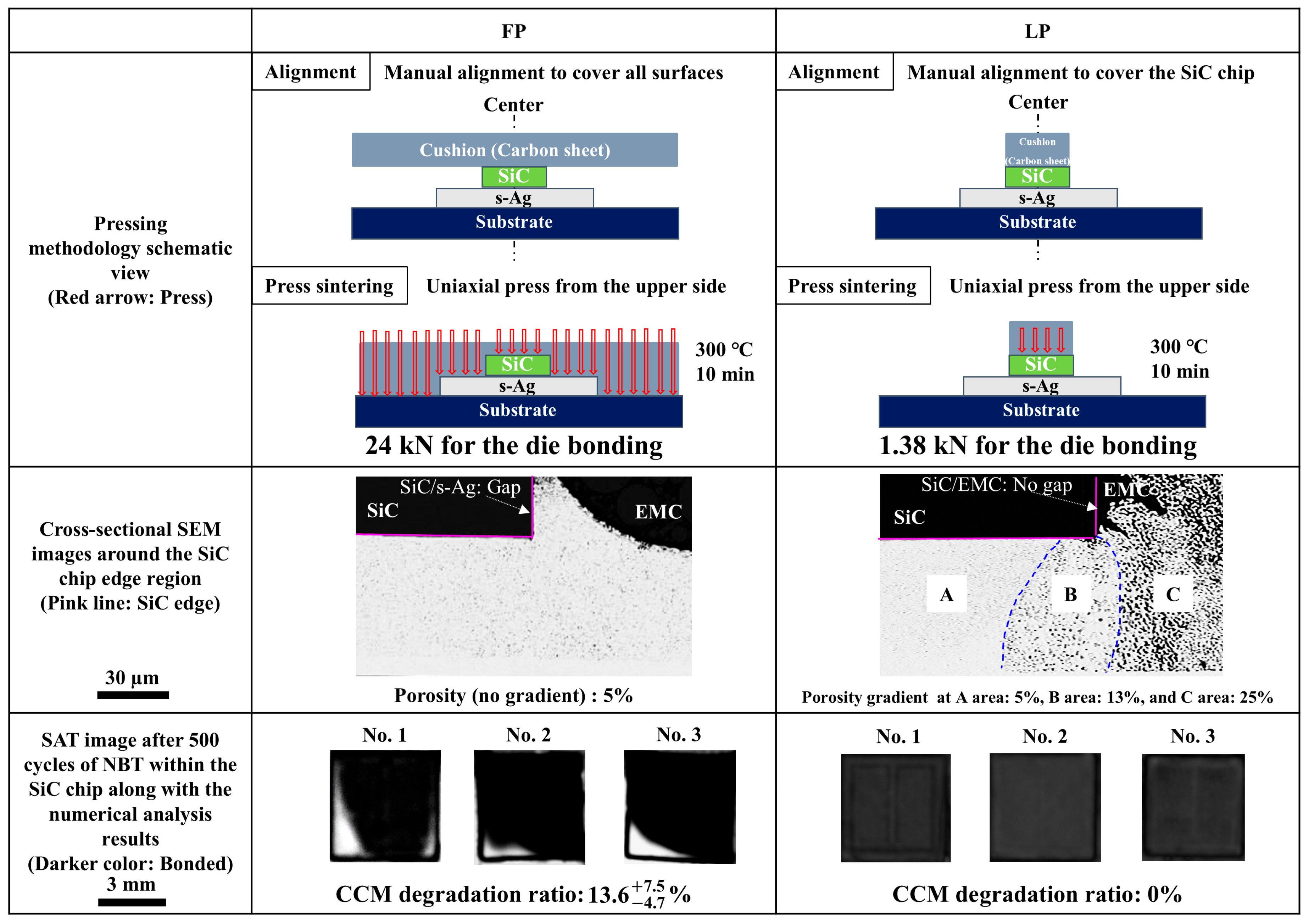
Figure 5 summarizes the differences between the FP and LP in terms of the pressing area control methodology, achievable porosity gradient, and CCM degradation within the SiC chip during the NBT, considering the obtained results. The LP method is a favorable method for DAAs. Although the applied force value in the LP was one-seventeenth of the applied force in the FP in the die bonding process, the CCM degradation ratio after the NBT was 0%, whereas the FP showed the CCM degradation ratio with 13.6 4.7 + 7.5 % after 500 cycles of the NBT. This CCM degradation ratio in the FP exceeds the rth by 15%, considering the relationship between the degradation ratio and thermal resistance in the previous study [23]. That is, the FP approaches the product lifetime defined as the rth of 20% [11].

4. Discussion

Based on the observation analysis results stated in the previous section, we investigated the stress distribution around the SiC chip’s bottom right corner. The main objective of this FEA is to determine the reason why the FP proceeded with the degradation of the pore growth and cracking in the s-Ag layer from 100 cycles of the NBT, whereas the LP showed no substantial damage in the s-Ag beneath the SiC chip up to 500 cycles of the NBT.
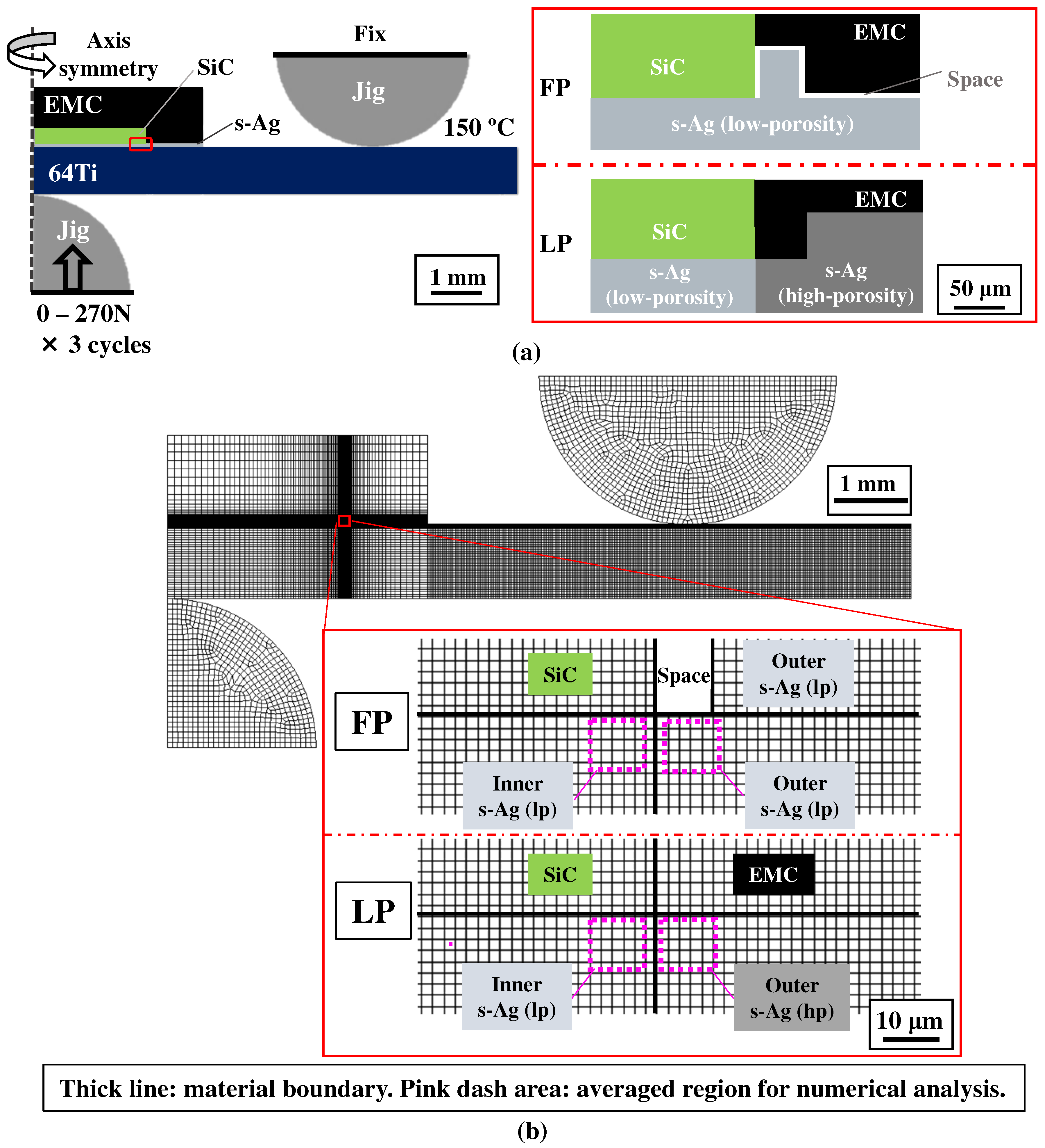
Figure 6a shows a schematic of the modeling and boundary conditions used for the FEA. For simplicity, we adopted two-dimensional (2D) FEA models, reflecting our experiment set up in the NBT. Note that this 2D model cannot illustrate the partial outer degradation effect on the inner delamination. However, we assumed that the inner degradation and outer degradation relationship is pivotal to considering the main cause of the degradation during the NBT. The model was produced using commercial software ANSYS 19.0. The axis-symmetric condition was set on the left edge of the model. A force variation of 270 N was set at the bottom line of the load jig. The calculation was implemented with three cycles of force variation to stabilize the FEA accuracy, as previously adopted [21]. The fix was set on the top line of the support jig. The ambient temperature was set to 150 °C. The model configuration around the SiC chip’s bottom right corner varies in the FP and LP, as shown in the red frame of Figure 6a, which corresponds to the cross-sectional observation results presented in Figure 3a and Figure 4. For the FP s-Ag layer’s pore distribution, the entire s-Ag part has the same material, with low-porosity (lp) s-Ag based on the top-line image in Figure 3a at the initial state. The gap was intentionally fabricated among the SiC, EMC, and s-Ag layers because the EMC delamination easily occurred due to the planarized interface during the NBT. In contrast, for the LP s-Ag layer pore distribution, the s-Ag layer is set to lp, with a high-porosity (hp) for the inner and outside of the SiC, respectively, based on the numerical analysis results of the third-line image in Figure 3b at the initial state. Note that the middle state of porosity exists from the edge to the inside with a 20 μm width, as shown in the second-line images of Figure 3b; however, in this FEA, we eliminated this layer because simplifying the model directly allows us to discuss the cause of the fracture mode difference between the FP and LP. The differences in material characteristics between the hp and lp s-Ag layers are considered by elucidating the S–S curves for the lp and hp s-Ag, as will be stated later. All interfaces have no gaps, as shown in Figure 3b and Figure 4.
Figure 6b shows the mesh pattern in the FEA and local numerical analysis region around the stress concentration area during the NBT. We adopted an almost quadrilateral shape of the mesh to stabilize the calculation. In the jig portion, we allowed the triangular mesh to fit the arc shape in the jig. The mesh size was biased to be a fine size to precisely calculate the stress concentration area, where the edge of the SiC, EMC, and s-Ag layer gathers, as shown in the red frame in Figure 6b. The bias pattern was identical to that in our previous study [18,31]. As observed from the enlarged view of the mesh pattern, the element size was regulated to 4 μm2. To avoid the singularity of the numerical analysis results, the averaged values at 74 nodes located within the pink dotted frame around the boundary were chosen in this study. To improve the numerical convergence, the force step number was regulated to 240 times in this FEA.
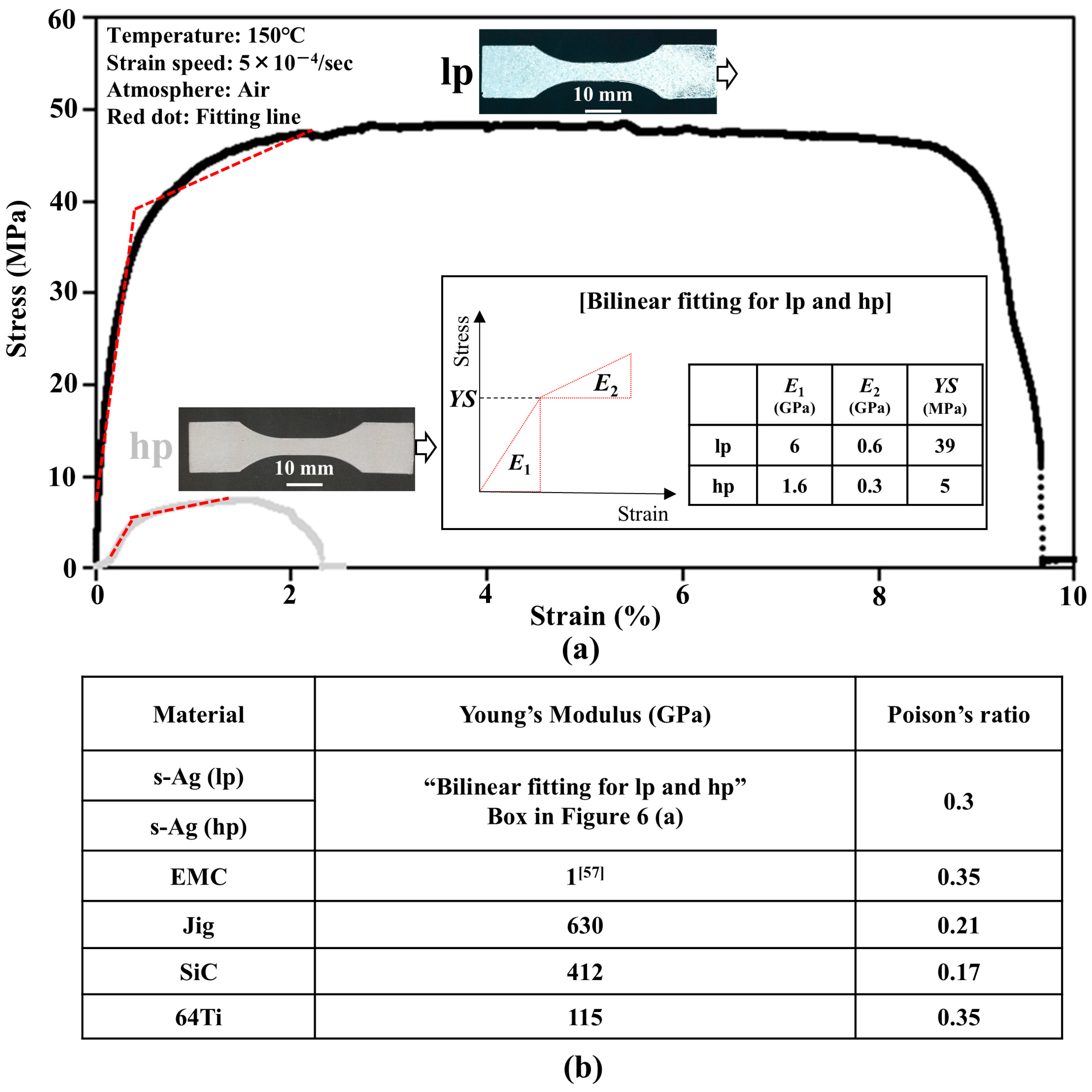
Among the materials used in PKG, the elastic–plastic properties of s-Ag at 150 °C must be considered in the lp and hp s-Ag when evaluating the APS precisely in this FEA. To model the elastic–plastic curve in the lp and hp s-Ag, we conducted uniaxial tensile film testing prior to the FEA. Figure 7a shows the obtained stress–strain (S–S) curves for the lp and hp s-Ag at 150 °C under the strain speed of 5 × 10⁻⁴/s. The lp and hp s-Ag specimens were sintered at 300 °C for 10 min under a 60 and 0.7 MPa pressure, respectively, to illustrate the lp and hp s-Ag porosity levels of 5 and 25%. The strain rate and test temperature were selected to match the NBT conditions. The tensile specimens were shaped into a dog-bone specimen and pulled in the direction indicated by the white arrows, as shown in the photographs in Figure 7a, as reported in our previous work [57]. Both S–S curves show nonlinear behavior, indicating that the lp and hp s-Ag fractured in a ductile manner. For the lp s-Ag, the linear trend associated with the elastic region ends at the applied stress of approximately 35 MPa, followed by a gradual reduction in the slope up to around 45 MPa. Beyond this point, the curve exhibits a broad plateau extending to approximately 6% to be fractured. For the hp, the linear trend ends at around 5 MPa, and the slope becomes gentle, with a gradual increase in stress up to 7 MPa before it declines toward the fracture. Both curves were fitted using bilinear kinematic curves, as were widely used in previous studies because of their simplicity and ability to accurately capture the material’s elastic–plastic properties [18,31,43,44]. In this study, the red dotted lines represent the bilinear fitting curves (S–S curves) for the lp and hp s-Ag. We defined the first slope of E1 in the stress range from 20% to 70% of the ultimate tensile stress. Since the clear yield stress (YS) is difficult to define in both lp and hp s-Ag curves, we defined the YS by the 0.2% offset method, which was applied for a porous metal material [58]. The second slope of E2 was defined as the slope of the S–S curves after the yield point, up to the point where the curve changes relatively linearly. The red dotted line represents an approximate line, used for the fitting to the obtained S–S curves. The numerical data used for the bilinear fitting are shown in the box of the “Bilinear fitting for lp and hp” in Figure 7a. The other elastic material input values are shown in Figure 7b.
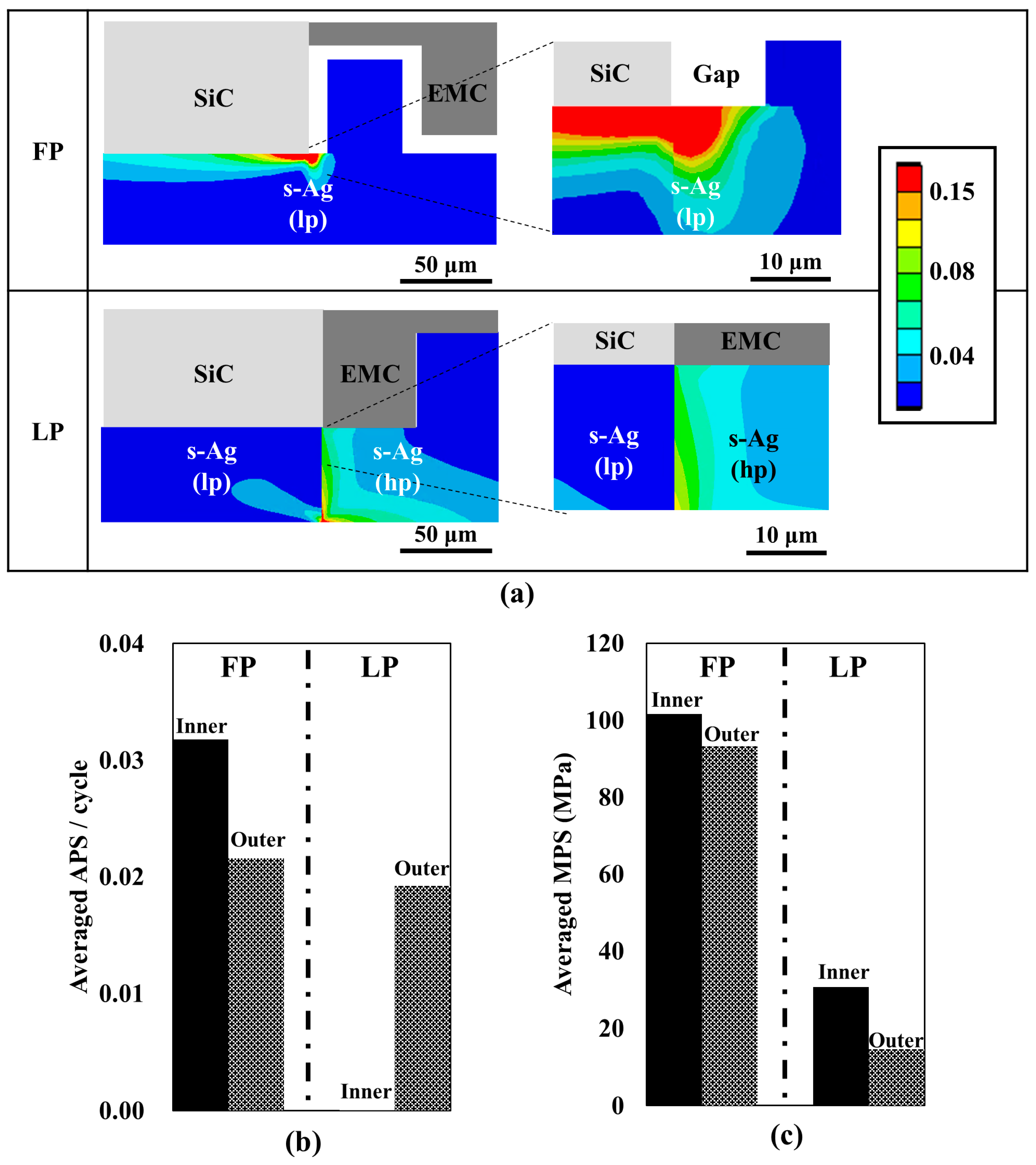
Figure 8a shows the APS distribution in the s-Ag layer for the FP and LP at three cycles of force applied in the NBT. The red zone represents the APS concentration. For the FP, a large APS value is locally distributed at the bottom right corner edge of the SiC chip next to the gap. From an enlarged image of this corner portion, the concentration area spreads approximately 20 × 5 μm2 around the corner of the SiC chip. This APS concentration caused s-Ag layer degradation, with cracking beneath the SiC chip and local pore growth outside of the SiC during the NBT. In contrast, the APS concentration in the LP was not found. The higher APS in the LP is located at the hp layer, which is located at the boundary between the lp and hp layer. The APS level was between 0.08 and 0.12, considering the enlarged results. This APS distribution was associated with the input mechanical property relationship between the lp and hp. Since Young’s modulus in the hp is lower than that in the lp, the APS in the hp s-Ag layer preferentially deforms by the applied stress during the NBT with increasing APS. As a result, the s-Ag in the hp entirely deforms to avoid the local APS concentration at the corner of the edge. This mild APS distribution contributed to avoiding damage in the s-Ag layer during the NBT.
To consider the CCM difference between the FP and LP quantitively, the average APS per cycle was compared in the local region, as is defined in Figure 6b. Figure 8b shows the bar graph of the average APS per cycle. The fill difference represents the difference in the average area of the inner and outer regions. The filled and hatched black refer to the average inner and outer areas of the SiC chip, respectively. For the FP, the value in the inner region is 0.032, which is approximately 1.5 times higher than that in the outer region. Since the FP’s s-Ag experienced plastic strain accumulation at this level during the applied force during the NBT, a crack inside the die layer was caused after 100 cycles of the NBT. In addition, this APS value level of 0.032 caused a CCM degradation during the NBT, which was confirmed by our previous results in which the CCM degradation ratio was 12% after 600 cycles of the NBT [31]. Therefore, the FEA result effectively reflects the CCM behavior and that the cracking of the s-Ag layer preferentially progressed inside the SiC chip during the NBT. In contrast, for the LP, the value relation between the inner and outer areas is contrary to the FP. The average APS per cycle value in the inner region was 6.5 × 10⁻⁶, meaning that the cracking damage risk during the NBT was almost zero for the s-Ag layer inside the SiC chip. As a result, the CCM was not observed during the NBT in the LP. The average APS per cycle value at the out region was 0.019, indicating that the damage risk existed outside the SiC chip for the LP during the NBT. However, this value did not cause continuous cracking outside the s-Ag layer. We confirmed that this drastic APS distribution along the boundary between the lp and hp layer suppressed the CCM of the s-Ag layer within the SiC chip during the NBT. In the previous study of conventional methods with a vertical pore gradient, the simulation analysis was limited to an elastic model, and the strain distribution within the joint layer was found to be contained within an approximately twofold magnitude. This is in significant contrast to the dramatic APS distribution we confirmed in this study. As a result, the degradation ratio improvement in the vertical pore gradient was limited to a maximum of 5% after the TST [49].
We also considered the s-Ag pore growth caution surrounding the SiC chip during the NBT based on the average maximum principal stress (MPS) because pore growth is associated with Ag grain boundary diffusion, which is accelerated by the applied stress [59,60]. Figure 8c shows the bar graph of the average MPS. The color scheme for the graphs is identical to that in Figure 8b. For the FP, the average MPS in the inner and outer regions was 102 and 93 MPa, respectively. As discussed above, cracking preferentially occurred inside the chip due to the 1.5 times higher APS per cycle value than that at the SiC chip’s outside area. Therefore, the average MPS value of 93 MPa is a target value to discuss the possibility of pore growth in the outside area under NBT conditions. The possibility of pore growth is considered based on our previous results of the pressurized s-Ag pore growth criterion map [31]. The input value for this pore growth equation assumes that the initial pore radius is the same because the sintering condition and paste are identical to those in the previous study. The aging time was set to 150,000 s, which corresponds to the 500 cycles of the NBT. As a result, the local average MPS caused pore growth outside the s-Ag layer in the FP. For the LP, the average MPS value inside the SiC chip was 31 MPa. This value is below the pore growth criterion plane, which coincides with no microstructure change in the s-Ag layer inside the SiC chip. In contrast, the average MPS value outside the SiC chip was 15 MPa, exceeding the ultimate tensile strength of 7 MPa of the lp s-Ag (Figure 7a). The Ag grains were located separately, similarly to the discontinuous cracking during the NBT (Figure 3b).
Preferential damage occurring outside the SiC chip helps maintain the Rth, as the degradation in this region does not affect the primary thermal path originating from the SiC chip. However, potential tradeoffs include the risk of interface delamination outside the s-Ag layer. When the interface force is weak between the non-pressed s-Ag and the substrate metal, a catastrophic interface fracture may occur during reliability testing. If these cracks allow air to infiltrate the PKG, oxygen exposure can alter the material properties or weaken the local bonding at the bottom corner region, creating new stress intensity points. To mitigate this risk, applying a barrier layer, such as Al2O3, to the outermost layer of the EMC is a promising approach [61,62].

5. Conclusions

This study investigated the suppression of the CCM beneath the semiconductor die using the NBT. Two pressurized types of s-Ag assemblies were used to control the porosity in the s-Ag layer. The FP showed both failure modes of the s-Ag layer degradation of the cracking beneath the SiC chip and EMC/s-Ag delamination from 100 cycles of the NBT. In contrast, the LP showed no such degradation up to 500 cycles of the NBT. The APS distribution in the s-Ag layer illustrates this fracture mode difference. For the FP, the APS distribution was locally concentrated at the corner of the SiC chip, which acted as an APS singularity point, leading to the CCM beneath the SiC chip in the s-Ag layer. In contrast, for the LP, the applied stress preferentially deformed the hp of the s-Ag layer due to the lower stiffness compared to that in the lp s-Ag layer. As a result, if the APS is not located concentrically at the s-Ag layer, any significant CCM beneath the SiC chip in the s-Ag layer can be avoided.
In summary, from the reliability design perspective, how we intentionally construct a deformable area in the PKG structure is especially important in protecting against the unfavorable CCM, such as horizontal cracks beneath the SiC chip. In this study, when the s-Ag porosity beneath the SiC is lower than that outside the SiC chip, the s-Ag layer’s cracking beneath the SiC chip can be stopped.
For future PKG reliability designs, the APS distribution obtained by the FEA is an essential step in predicting the danger zone during reliability tests. However, we should elucidate the model configuration validation, whether it is a continuous structure or not. In particular, the interface in the PKG should be considered carefully because the interface commonly loses its perfect connection due to local defects. Elucidating the morphology and quantifying the toughness of each interface should be a priority. We will integrate the interface evaluation results and the reliability results to develop a comprehensive reliability design in PKG. Additionally, we will investigate the different combinations of PKG and reliability tests to elucidate the validity of the reliable LP potential. Our research limits the reliability evaluation to the TST mode only. However, we will also clarify the aging effect (e.g., humidity) on the degradation of the PKG to explore the potential of the LP for practical case universality.

Author Contributions

Conceptualization, K.W. and K.N.; methodology, K.W.; software, K.W.; validation, K.W.; formal analysis, K.W.; investigation, K.W., M.U., and A.S.; resources, K.W., M.U., and A.S.; data curation, K.W.; writing—original draft preparation, K.W.; writing—review and editing, K.W. and K.N.; visualization, K.W.; supervision, K.N.; project administration, K.W. and K.N. All authors have read and agreed to the published version of the manuscript.

Funding

This research received no external funding.

Data Availability Statement

The original contributions presented in this study are included in the article. Further inquiries can be directed to the corresponding author.

Conflicts of Interest

All authors are employed by the company ROHM Co., Ltd. and they declare that the research was conducted in the absence of any commercial or financial relationships that could be construed as a potential conflict of interest.

Abbreviations

CCMCohesive cracking mode
IDMInterface delamination mode
s-AgSintered silver
hpHigh-porosity
lpLow-porosity
FPFull press
LPLocal press
DAAsDie-attached assemblies
WBGWide band gap
SiCSilicon carbide
NBTNine-point bending test
TSTThermal shock test
APSAccumulated plastic strain
PKGPackaging
EMCEpoxy molding compounds
CTECoefficients of thermal expansion
RthThermal resistance of the PKG
rthRth increase ratio
SATScanning acoustic tomography
2DTwo dimensional
FEAFinite element analysis
BSEBackscattering elecron
SEMScanning electron microscopy
S–SStress–strain
YSYield stress
MPSMaximum principal stress

References

  1. Sprenger, M.; Forndran, F.; Ottinger, B.; Braum, T.; Franke, J. Reliability assesment and thermal characterization of automotive power module package based on novel thick copper-ceramic substrate and hard epoxy encapsulation. In Proceedings of the 12th International Conference on Integrated Power Electronics Systems (CIPS), Berlin, Germany, 15–17 March 2022. [Google Scholar]
  2. Emon, A.I.; Hassan, M.U.; Mirza, A.B.; Narayanasamy, B.; Luo, F. A Figure of Merit for SiC MOSFET Power Modules to Achieve High Power-Density Energy Conversion. IEEE Trans. Electron. Devices 2023, 70, 3718–3725. [Google Scholar] [CrossRef]
  3. Hudgins, J.L.; Simin, G.S.; Santi, E.; Khan, M.A. An assessment of wide bandgap semiconductors for power devices. IEEE Trans. Power Electron. 2003, 18, 907–914. [Google Scholar] [CrossRef]
  4. Biela, J.; Schweizer, M.; Waffler, S.; Kolar, J.W. SiC versus Si—Evaluation of Potentials for Performance Improvement of Inverter and DC–DC Converter Systems by SiC Power Semiconductors. IEEE Trans. Ind. Electron. 2011, 58, 2872–2882. [Google Scholar] [CrossRef]
  5. Peng, P.; Hu, A.; Gerlich, A.P.; Zou, G.; Liu, L.; Zhou, Y.N. Joining of Silver Nanomaterials at Low Temperatures: Processes, Properties, and Applications. ACS Appl. Mater. Interfaces 2015, 7, 12597–12618. [Google Scholar] [CrossRef] [PubMed]
  6. Siow, K.S. Are Sintered Silver Joints Ready for Use as Interconnect Material in Microelectronic Packaging? J. Electron. Mater. 2014, 43, 947–961. [Google Scholar] [CrossRef]
  7. Chen, C.-J.; Chen, C.-M.; Horng, R.-H.; Wuu, D.-S.; Hong, J.-S. Thermal Management and Interfacial Properties in High-Power GaN-Based Light-Emitting Diodes Employing Diamond-Added Sn-3 wt.%Ag-0.5 wt.%Cu Solder as a Die-Attach Material. J. Electron. Mater. 2010, 39, 2618–2626. [Google Scholar] [CrossRef]
  8. Youssef, T.; Rmili, W.; Woirgard, E.; Azzopardi, S.; Vivet, N.; Martineau, D.; Meuret, R.; Le Quilliec, G.; Richard, C. Power modules die attach: A comprehensive evolution of the nanosilver sintering physical properties versus its porosity. Microelectron. Reliab. 2015, 55, 1997–2002. [Google Scholar] [CrossRef]
  9. Ordonez-Miranda, J.; Hermens, M.; Nikitin, I.; Kouznetsova, V.G.; van der Sluis, O.; Ras, M.A.; Reparaz, J.S.; Wagner, M.R.; Sledzinska, M.; Gomis-Bresco, J.; et al. Measurement and modeling of the effective thermal conductivity of sintered silver pastes. Int. J. Therm. Sci. 2016, 108, 185–194. [Google Scholar] [CrossRef]
  10. Lv, W.; Liu, J.; Lei, X.; Zhu, F. Porosity Dependence of Thermal and Electrical Properties in Nano-Silver Paste. IEEE Trans. Electron. Devices 2023, 70, 702–707. [Google Scholar] [CrossRef]
  11. ECPE Guideline AQG 324: Qualification of Power Modules for Use in Power Electronics Converter Units in Motor Vehicles; ECPE European Center for Power Electronics e.V.: Nuremberg, Germany, 2019.
  12. Wilde, J.; Staiger, W.; Thoben, M.; Schuch, B.; Kilian, H. Integration of Liquid Cooling, Thermal and Thermomechanical Design for the Lifetime Prediction of Electrical Power Modules. In Proceedings of the International Congress and Exposition, Detroit, MI, USA, 23–26 February 1998. [Google Scholar]
  13. Wakamoto, K.; Otsuka, T.; Nakahara, K.; Namazu, T. Degradation Mechanism of Pressure-Assisted Sintered Silver by Thermal Shock Test. Energies 2021, 14, 5532. [Google Scholar] [CrossRef]
  14. Wakamoto, K.; Kumakiri, Y.; Otsuka, T.; Nakahara, K.; Namazu, T. Comparison of sintered silver die attach failure between thermal shock test and mechanical cycling test. Jpn. J. Appl. Phys. 2022, 61, SD1029. [Google Scholar] [CrossRef]
  15. Herboth, T.; Guenther, M.; Fix, A.; Wilde, J. Failure Mechanisms of Sintered Silver Interconnections for Power Electronic Applications. In Proceedings of the 63rd Electronic Components and Technology Conference (ECTC), Las Vegas, NV, USA, 28–31 May 2013. [Google Scholar]
  16. Henaff, F.L.; Azzopardi, S.; Woirgard, E.; Youssef, T.; Bontemps, S.; Joguet, J. Lifetime Evaluation of Nanoscale Silver Sintered Power Modules for Automotive Application Based on Experiments and Finite-Element Modeling. IEEE Trans. Device Mat. Rel. 2015, 15, 326–334. [Google Scholar] [CrossRef]
  17. Sugiura, K.; Iwashige, T.; Tsuruta, K.; Chen, C.; Nagao, S.; Funaki, T. Reliability Evaluation of SiC Power Module with Sintered Ag Die Attach and Stress-Relaxation Structure. IEEE Trans. Compon. Packag. Manuf. Technol. 2019, 9, 609–615. [Google Scholar] [CrossRef]
  18. Wakamoto, K.; Fuji, K.; Otsuka, T.; Nakahara, K.; Namazu, T. Nine Point Bending Test Technique for Understanding of Sintered Silver Die Bonding Failure Mechanism. Exp. Tech. 2024, 48, 399–408. [Google Scholar] [CrossRef]
  19. Zhang, Z.; Chen, C.; Suetake, A.; Hsieh, M.-C.; Suganuma, K. Reliability of Ag Sinter-Joining Die Attach Under Harsh Thermal Cycling and Power Cycling Tests. J. Electron. Mater. 2021, 50, 6597–6606. [Google Scholar] [CrossRef]
  20. Qin, F.; Hu, Y.; Dai, Y.; An, T.; Chen, P.; Gong, Y.; Yu, H. Crack Effect on the Equivalent Thermal Conductivity of Porously Sintered Silcer. J. Electron. Mater. 2020, 49, 5994–6008. [Google Scholar] [CrossRef]
  21. Gorecki, P.; Gorecki, K.; Kisiel, R.; Brzozowski, E.; Bar, J.; Guziewicz, M. Investigations of an Influence of the Assembling Method of the Die to the Case on Thermal Parameters of IGBTs. IEEE Trans. Compon. Packag. Manuf. Technol. 2021, 11, 1988–1996. [Google Scholar] [CrossRef]
  22. Dai, J.; Li, J.; Agyakwa, P.; Corfield, M.; Johnson, C.M. Comparative Thermal and Structural Characterization of Sintered Nano-Silver and High-Lead Solder Die Attachments During Power Cycling. IEEE Trans. Device Mater. Reliab. 2018, 18, 256–265. [Google Scholar] [CrossRef]
  23. Liu, S.; Vuorinen, V.; Liu, X.; Fredrikson, O.; Brand, S.; Tiwary, N. Fatigue Crack Networks in Die-Attach Layers of IGBT Modules Under a Power Cycling Test. IEEE Trans. Power Electron. 2024, 39, 16695–16707. [Google Scholar] [CrossRef]
  24. Huang, Y.; Luo, Y.; Xiao, F.; Liu, B. Failure Mechanism of Die-Attach Solder Joints in IGBT Modules Under Pulse High-Current Power Cycling. IEEE J. Emerg. Sel. Top. Power Electron. 2019, 7, 99–107. [Google Scholar] [CrossRef]
  25. Wunderle, B.; Becker, K.F.; Sinning, R.; Wittler, O.; Schacht, R.; Walter, H.; Schneider-Ramelow, M.; Halser, K.; Simper, N.; Michel, B.; et al. Thermo-mechanical reliability during technology development of power chip-on-board assemblies with encapsulation. Microsyst. Technol. 2009, 15, 1467–1478. [Google Scholar] [CrossRef]
  26. Heilmann, J.; Nikitin, I.; Zschenderlein, U.; May, D.; Pressel, K.; Wunderle, B. Reliability experiments of sintered silver based interconnections by accelerated isothermal bending tests. Microelectron. Reliab. 2017, 74, 136–146. [Google Scholar] [CrossRef]
  27. Forndran, F.; Heilmann, J.; Metzler, M.; Leicht, M.; Wunderle, B. Determination of Rate- and Temperature Dependent Inelastic Material Data for Sintered Silver Die Attach and Simulative Implementation. In Proceedings of the 23rd International Conference on Thermal, Mechanical and Multi-Physics Simulation and Experiments in Microelectronics and Microsystems (EuroSimE), St. Julian, Malta, 25–27 April 2022. [Google Scholar]
  28. Heilmann, J.; Wunderle, B.; Zschenderlein, U.; Wille, C.; Pressel, K. Physics of failure based lifetime modelling for sintered silver die attach in power electronics: Accelerated stress testing by isothermal bending and thermal shock in comparison. Microelectron. Reliab. 2023, 145, 114973. [Google Scholar] [CrossRef]
  29. Wakamoto, K.; Mochizuki, Y.; Otsuka, T.; Nakahara, K.; Namazu, T. Temperature Dependence on Tensile Mechanical Properties of Sintered Silver Film. Materials 2020, 13, 4061. [Google Scholar] [CrossRef] [PubMed]
  30. Wakamoto, K.; Yasugi, D.; Otsuka, T.; Nakahara, K.; Namazu, T. Fracture Mechanism of Sintered Silver Film Revealed by In Situ SEM Uniaxial Tensile Loading. IEEE Trans. Compon. Packag. Manuf. Technol. 2024, 14, 240–250. [Google Scholar] [CrossRef]
  31. Wakamoto, K.; Otsuka, T.; Nakahara, K.; Mugilgeethan, V.; Matsumoto, R.; Namazu, T. Degradation Mechanism of Silver Sintering Die Attach Based on Thermal and Mechanical Reliability Testing. IEEE Trans. Compon. Packag. Manuf. Technol. 2023, 13, 197–210. [Google Scholar] [CrossRef]
  32. Herboth, T.; Fruh, C.; Gunther, M.; Wilde, J. Assessment of Thermo-Mechanical Stresses in Low Temperature Joining Technology. In Proceedings of the 13th International Thermal, Mechanical and Multi-Physics Simulation and Experiments in Microelectronics and Microsystems (EurosimE), Cascais, Portugal, 16–18 April 2012. [Google Scholar]
  33. Gadaud, P.; Caccuri, V.; Bertheau, D.; Carr, J.; Milhet, X. Ageing sintered silver: Relationship between tensile behavior, mechanical properties and the nanoporous structure evolution. Mater. Sci. Eng. A 2016, 669, 379–386. [Google Scholar] [CrossRef]
  34. Nikitin, I.; Pressel, K. Mechanical Properties of Porous Silver Materials Depending on Sintering Parameters, In Proceedings of the 20th International Workshop on Thermal Investigations of ICs and Systems (THERMINIC), Greenwich, UK, 24–26 September 2014.
  35. Ng, W.C.W.; Seatman, K.; Kumagai, K.; Takamura, K.; Nishimura, T.; Letz, S.; Schletz, A. The correlation between sintered silver joint reliability and pressure assisted sintering parameters. In Proceeding of the 19th Electronics Packaging Technology Conference (EPTC), Shingapore, 6–9 December 2017. [Google Scholar]
  36. Zabihzadeh, S.; Van Petegem, S.; Holler, M.; Diaz, A.; Duarte, L.I.; Van Swygenhoven, H. Deformation behavior of nanoporous polycrystalline silver. Part I: Microstructure and mechanical properties. Acta Mater. 2017, 131, 467–474. [Google Scholar] [CrossRef]
  37. Fan, J.; Xu, D.; Zhang, H.; Qian, C.; Fan, X.; Zhang, G. Experimental Investigation on the Sintering Kinetics of Nanosilver Particles Used in High-Power Electronic Packaging. IEEE Trans. Compon. Packag. Manuf. Technol. 2020, 10, 1101–1109. [Google Scholar] [CrossRef]
  38. Xu, Y.; Qiu, X.; Li, W.; Wang, S.; Ma, N.; Ueshima, M.; Chen, C.; Suganuma, K. Development of high thermal conductivity of Ag/diamond composite sintering paste and its thermal shock reliability evaluation in SiC power modules. J. Mater. Res. Technol. 2023, 26, 1079–1093. [Google Scholar] [CrossRef]
  39. Zhang, H.; Nagao, S.; Suganuma, K. Addition of SiC Particles to Ag Die-Attach Paste to Improve High-Temperature Stability; Grain Growth Kinetics of Sintered Porous Ag. J. Electron. Mater. 2015, 44, 3896–3903. [Google Scholar] [CrossRef]
  40. Heuck, N.; Langer, A.; Stranz, A.; Palm, G.; Sittig, R.; Bakin, A.; Waag, A. Analysis and Modeling of Thermomechanically Improved Silver-Sintered Die-Attach Layers Modified by Additives. IEEE Trans. Compon. Packag. Manuf. Technol. 2011, 1, 1846–1855. [Google Scholar] [CrossRef]
  41. Wakamoto, K.; Kumakiri, Y.; Namazu, T. Mechanical property changes in sintered silver films by including copper oxide nanoparticles. Microelectron. Reliab. 2024, 153, 115322. [Google Scholar] [CrossRef]
  42. Lv, W.; Liu, J.; Mou, Y.; Ding, Y.; Chen, M.; Zhu, F. Fabrication and sintering behavior of nano Cu-Ag composite paste for high-power device. IEEE Trans. Electron. Devices 2023, 70, 3202–3207. [Google Scholar] [CrossRef]
  43. Rajaguru, P.; Lu, H.; Bailey, C. Sintered silver finite element modelling and reliability based design optimisation in power electronic module. Microelectron. Reliab. 2015, 55, 919–930. [Google Scholar] [CrossRef]
  44. Forndran, F.; Heilmann, J.; Metzler, M.; Leicht, M.; Wunderle, B. A Parametric Simulative Study for Lifetime Prediction of Sintered Silver Die Attach Under Different Accelerated Testing Conditions. In Proceedings of the 22nd International Conference on Thermal, Mechanical and Multi-Physics Simulation and Experiments in Microelectronics and Microsystems (EuroSimE), St. Julian, Malta, 19–21 April 2021. [Google Scholar]
  45. Weidler, J.; Newman, R.; Zhai, C.J. Optimizing assembly factors to minimize interlayer die stress in a PBGA package. In proceeding of the 52nd Electronic Components and Technology Conference (ECTC), San Diego, CA, USA, 28–31 May 2002. [Google Scholar]
  46. Manikam, V.R.; Paing, S.; Ang, A. Effects of soft solder materials and die attach process parameters on large power semiconductor dies joint reliability. In Proceedings of the 15th Electronics Packaging Technology Conference (EPTC), Singapore, 11–13 December 2013. [Google Scholar]
  47. Schaal, M.; Klingler, M.; Metais, B.; Gruninger, R.; Hoffmann, S.; Wunderle, B. Reliability Assessment of Ag Sintered Joints Using a SiC Semiconductor and Determination of Failure Mechanism in the Field of Power Electronics. In Proceedings of the 21st International Conference on Thermal, Mechanical and Multi-Physics Simulation and Experiments in Microelectronics and Microsystems (EuroSimE), Cracow, Poland, 5–8 July 2020. [Google Scholar]
  48. Zhao, Z.; Zou, G.; Zhang, H.; Ren, H.; Liu, L.; Zhou, Y.N. The mechanism of pore segregation in the sintered nano Ag for high temperature power electronics applications. Materaial Lett. 2018, 228, 168–171. [Google Scholar] [CrossRef]
  49. Zhang, B.; Zhang, S.; Lu, X.; Han, L.; Mei, Y.-H. Reliability Improvement of Low-Temperature Sintered Nano-Silver as Die Attachment by Porosity Optimization. IEEE Trans. Compon. Packag. Manuf. Technol. 2023, 13, 1209–1216. [Google Scholar] [CrossRef]
  50. Weerasing, H.C.; Sirimanne, P.M.; Simon, G.P.; Cheng, Y.-B. Cold isostatic pressing technique for producing highly efficient flexible dye-sensitised solar cells on plastic substrates. Prog. Photovolt Res. Appl. 2012, 20, 321–332. [Google Scholar] [CrossRef]
  51. Oh, C.; Nagao, S.; Suganuma, K. Silver stress migration bonding driven by themomechanical stress with various substrates. J. Mater. Sci. Mater. Electron. 2015, 26, 2525–2530. [Google Scholar] [CrossRef]
  52. Liu, Y.; Zhang, H.; Wang, L.; Fan, X.; Zhang, G. Effect of Sintering Pressure on the Porosity and the Shear Strength of the Pressure-Assisted Silver Sintering Bonding. IEEE Trans. Device Mater. Reliab. 2018, 18, 240–246. [Google Scholar] [CrossRef]
  53. Bajwa, A.A.; Zeiser, R.; Wilde, J. Process optimization and characterization of a noverl micro-scaled silver sintering paste as a die-attach material for high temperature high power semiconductor devices. In Proceedings of the 36th Electronic Components and Technology Conference (ISSE), Alba lulia, Romania, 8–12 May 2013. [Google Scholar]
  54. Wakamoto, K.; Mochizuki, Y.; Otsuka, T.; Nakahara, K.; Namazu, T. Tensile mechanical properties of sintered porous silver films and their dependence on porosity. Jpn. J. Appl. Phys. 2019, 58, SDDL08. [Google Scholar] [CrossRef]
  55. Wang, M.; Mei, Y.; Li, X.; Burgos, R.; Boroyevich, D.; Lu, G.-Q. How to determine surface roughness of copper substrate for robust pressureless sintered silver in air. Mater. Lett. 2018, 228, 327–330. [Google Scholar] [CrossRef]
  56. Chen, C.; Gao, Y.; Liu, Z.-Q.; Suginima, K. 3D pyramid-shape Ag plating assisted interface connection growth of sinter micron-sized Ag paste. Scr. Mater. 2020, 179, 36–39. [Google Scholar] [CrossRef]
  57. Ukita, M.; Wakamoto, K.; Nakahara, K. Increased high-temperature stifness of an epoxy-based molding compound through high-temperature storage. Microelectron. Reliab. 2025, 166, 115605. [Google Scholar] [CrossRef]
  58. Rakesh, P.; Pal, B. Finite element analysis of Ti6Al4V porous structure for low-stiff hip implant application. Int. J. Simul. Multidisci. Des. Optim. 2021, 12, 12. [Google Scholar] [CrossRef]
  59. Onaka, S.; Kato, M.; Soeta, S.; Mori, T. A New Approach for Diffusional Growth of Grain-Boundary Voids. Trans. Jpn. Inst. Met. 1988, 29, 284–291. [Google Scholar] [CrossRef]
  60. Onaka, S.; Kato, M. Unified Analysis for Various Diffusion-controlled Deformation and Fracture Processes. ISIJ Int. 1991, 31, 331–341. [Google Scholar] [CrossRef]
  61. Han, Y.C.; Kim, E.; Kim, W.; Im, H.-G.; Bae, B.-S.; Choi, K.C. A flexible moisture barrier comprised of a SiO2-embedded organic-inorganic hybrid nanocomposite and Al2O3 for thin-film encapsulation of OLEDs. Org. Electron. 2013, 14, 1435–1440. [Google Scholar] [CrossRef]
  62. Kwon, J.H.; Jeong, E.G.; Jeon, Y.; Kim, D.-G.; Lee, S.; Choi, K.C. Design of Highly Water Resistant, Impermeable, and Flexible Thin-Film Encapsulation Based on Inorganic/Organic Hybrid Layers. ACS Appl. Mater. Interfaces 2019, 11, 3251–3261. [Google Scholar] [CrossRef] [PubMed]
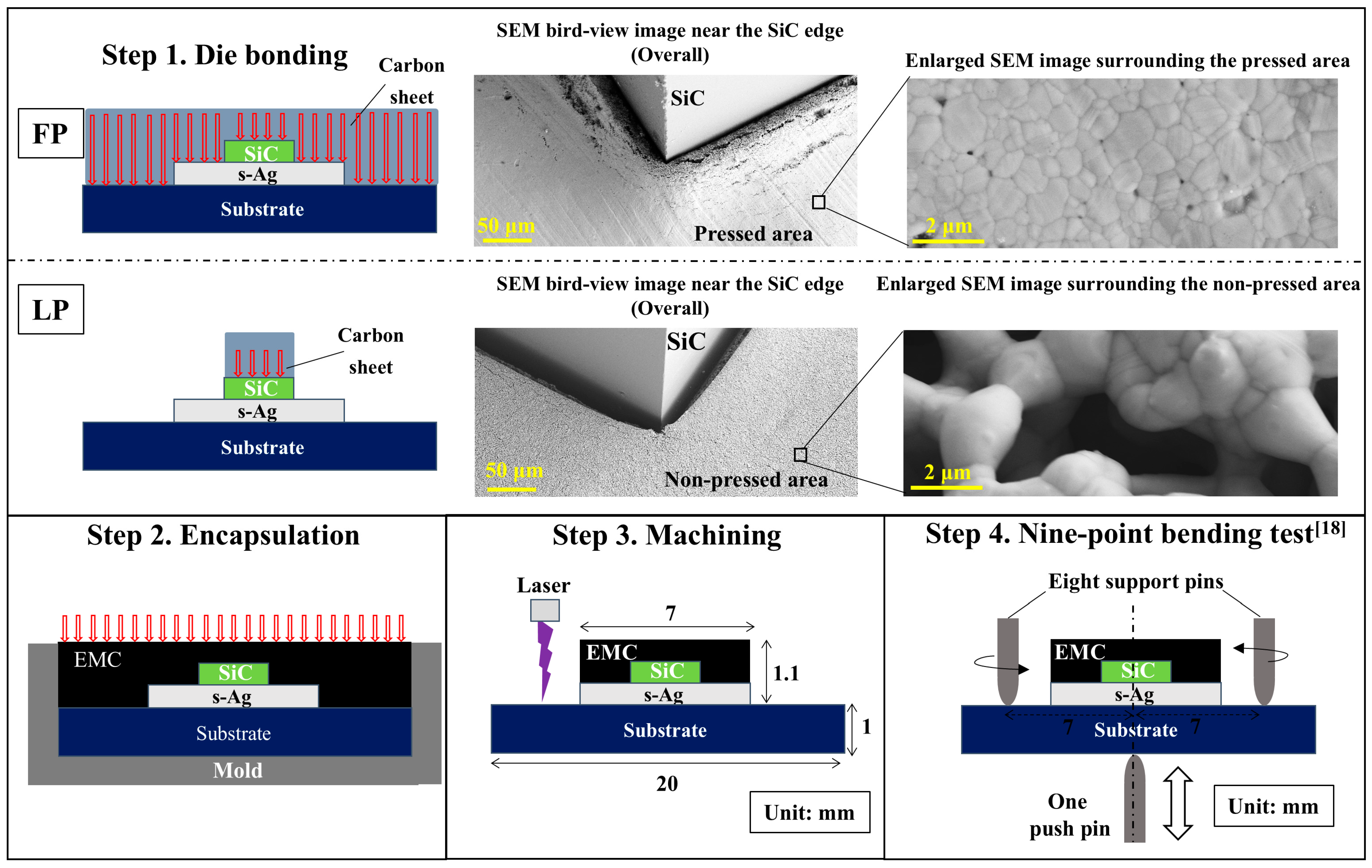
Figure 1. A schematic of the experimental procedure along with bird-view SEM images after the die bonding process.
Electronics 14 03227 g001
Figure 2. (a) Scanning acoustic tomography images of the FP and LP after the NBT. (Red frame: die area. Darker color: bonded area. Lighter color: degradation area.) (b) Numerical analysis results with the degradation ratio after 500 cycles of the NBT in the FP and LP. The bar graph shows the FP results of the degradation ratio after 500 cycles to illustrate the full data variability, representing the maximum and minimum values.
Electronics 14 03227 g002
Figure 3. Cross-sectional SEM images for (a) FP and (b) LP at initial state and after 100 and 500 cycles of NBT. (First line: overall image. Second line: enlarged image near SiC chip. Third line: microporous structure of s-Ag within blue square region in second-line images. Fourth line: enlarged area at EMC/s-Ag. Fifth line: reinforced edge image of forth-line images.)
Electronics 14 03227 g003aElectronics 14 03227 g003b
Figure 4. An enlarged view of cross-sectional SEM images around the side SiC chip for the FP and LP after 100 cycles of the NBT. Top-line images indicate the reinforced edge images. (Purple line: edge line.).
Electronics 14 03227 g004
Figure 5. The differences between the FP and LP in terms of the pressing area control methodology, achievable porosity gradient, and CCM degradation within the SiC chip during the NBT, considering the obtained results.
Electronics 14 03227 g005
Figure 6. (a) The simulation model configuration and boundary condition. (Red frame: the enlarged view of the edge around the SiC chip.) (b) The mesh condition along with an enlarged mesh view to illustrate the numerical analysis region.
Electronics 14 03227 g006
Figure 7. (a) S–S curves for lp and hp s-Ag at 150 °C along with bilinear fitting line and coefficients in lp and hp s-Ag. (b) Input mechanical properties for FEA.
Electronics 14 03227 g007
Figure 8. (a) FEA results of the APS distribution at three cycles of the s-Ag layer along with the FP and LP model. A bar graph of the (b) average APS per cycle and (c) the average MPS at the evaluated area.
Electronics 14 03227 g008
Table 1. Detailed experiment conditions, including tester or material and their specification or conditions.
StepTester or MaterialSpecification or condition
1Nano silver paste (commercial product)- 18 nm in diameter
1Carbon sheet (TOYO TANSO, VVF30, Osaka, Japan)- FP: 20 mm square, LP: 4.8 mm square, thickness: 1.6 mm
1Uniaxial press machine (SHINTOKOGIO, Ltd., CYPM-200, Aichi, Japan)- 60 MPa pressure for 10 min at 300 °C
2EMC (commercial product)- Silica filler 88 wt% (20 nm–40 μm in diameter)
- Biphenyl type epoxy resin
2Compression molding machine (TOWA, CPM-1080, Kyoto, Japan)- 13.8 MPa pressure
- Cure: 2 min at 165 °C
2Thermal chamber (ESPEC, ST-120, Osaka, Japan)- Air atmosphere
- Post-mold cure: 5 h at 175 °C
3Laser marker (KEYENCE, MD-U1000C, Osaka, Japan)- Ultraviolet laser (λ = 355 nm) of Gaussian beam profile
4Universal test system (Instron Japan, 68TM-5, Kanagawa, Japan)- In air atmosphere at 150 °C
- Force control (0 and 270 N under triangle waveform)
- 500 cycles
Disclaimer/Publisher’s Note: The statements, opinions and data contained in all publications are solely those of the individual author(s) and contributor(s) and not of MDPI and/or the editor(s). MDPI and/or the editor(s) disclaim responsibility for any injury to people or property resulting from any ideas, methods, instructions or products referred to in the content.