Article

Data Sampling System for Processing Event Camera Data Using a Stochastic Neural Network on an FPGA

by
Seth Shively
1,
Nathaniel Jackson
1,
Eugene Chabot
2,3,
John DiCecco
2,3 and
Scott Koziol
1,*
1
Electrical and Computer Engineering Department, Baylor University, Waco, TX 76798, USA
2
Naval Undersea Warfare Center, Newport, RI 02841, USA
3
Electrical, Computer & Biomedical Engineering, University of Rhode Island, Kingston, RI 02881, USA
*
Author to whom correspondence should be addressed.
Electronics 2025, 14(15), 3094; https://doi.org/10.3390/electronics14153094
Submission received: 4 July 2025 / Revised: 26 July 2025 / Accepted: 26 July 2025 / Published: 2 August 2025
(This article belongs to the Section Circuit and Signal Processing)

Abstract

The use of a stochastic artificial neural network (SANN) implemented on a Field Programmable Gate Array (FPGA) provides a promising method of performing image recognition on event camera recordings, however, challenges exist due to the fact that event camera data has an inherent unevenness in the timing at which data is sent out of the camera. This paper proposes a sampling system to overcome this challenge, by which all “events” occurring at specific timestamps in an event camera recording are selected (sampled) to be processed and sent to the SANN at regular intervals. This system is implemented on an FPGA in SystemVerilog, and to test it, simulated event camera data is sent to the system from a computer running MATLAB (version 2022+). The sampling system is shown to be functional. Analysis is shown demonstrating its performance regarding data sparsity, time convergence, normalization, repeatability, range, and some characteristics of the hold system.

1. Introduction and Background

Event cameras have shown to be effective in image processing [1]. For example, they have been used for space situational awareness [2], robotics [3,4], object detection and tracking [5,6], and driver assistance systems [7]. Field Programmable Gate Array (FPGA) systems, another important aspect of this work, also have wide applications. For example, FPGA technology is now widely applied in biomedical ultrasound [8] and industrial automation [9,10]. Event cameras have been designed to use an output protocol called “Address-event representation” (AER) [11]. Event camera data using AER is sent in packages containing information about each event, which, in some camera designs, is sent over a serial port to whichever device is reading the data.

1.1. Problem Addressed by This Paper

The problem with broad application being addressed by this paper, shown in Figure 1, is this: How does one connect the AER serial output data from an event camera with a stochastic computing neural network implemented in Field Programmable Gate Array (FPGA) hardware?
The neural network (NN) implemented on the FPGA is a stochastic artificial neural network (SANN) [12,13]. A SANN, of our design, has an input node for each pixel in the camera, Figure 1. An advantage of the sampling system described in this paper is that it is specifically designed to work with a SANN. This provides, in practice, a way to test stochastic computing processing of event camera data. This might result in stochastic computing advantages such as low-complexity computation circuits and error tolerance [14].
To accomplish the camera-SANN connection, the AER data needs to be translated by the FPGA back into parallel bitstreams corresponding to camera pixels. This paper addresses the camera-SANN connection with the goal of avoiding potential timing irregularities inherent in the data format. A solution to this challenge proposed in this paper is to create a sampling system which sets up a regular sampling period at which to clock the neural network running on the FPGA. An earlier paper describing SANN processing in an FPGA includes [12], and the specific solution of this paper is described in greater detail in [13] and also briefly described in [15].

1.2. Comparison with Existing Camera Data Processing Methods

While this system is designed for use with a SANN, it shares some similarities with existing data pre-processing methods used in other methods of image classification using machine learning, several of which are discussed below, and summarized in Table 1. Most methods use a technique called “frame accumulation”. Frame accumulation involves taking a set of events and combining them into a single static image, with each pixel value dependent on the position and frequency of events in the subset [16]. Two methods of frame accumulation exist: time-based and quantity-based [16]. The former takes a subset of events which occurred during a fixed time interval for which to perform the frame accumulation, whereas the latter picks subsets with a fixed number of events, regardless of the timing during which those events occurred [16]. Similarly to the system described in this paper, the latter approach only considers data associated with actual events into its calculations and does not take time gaps (at which no events occur) into account.
The frames generated by frame accumulation can themselves be processed using neural networks. One popular choice for this application is the spiking neural network [17]. A spiking neural network performs image classification on a series of accumulated event data frames, which may or may not be formed with overlapping data [18]. Another method involves “event tensors”, or 3D arrays of accumulated frames, which are converted into static images using an auto-encoder spiking neural network and then classified using a traditional (non-spiking, non-stochastic) neural network [19]. Yet another method involves using a traditional convolutional neural network (CNN) to perform image recognition on individual accumulated frames [20].
One event data processing method described by Viale et. al. using frame accumulation with a spiking neural network is similar to the method described in this paper. In Viale’s method, a fixed sampling rate was set, and all events occurring during each time interval were accumulated into frames, which were then used as input to the spiking neural network [17]. This method is fairly similar to the method proposed in this paper, except that in the method proposed here, events occurring at only one timestamp are sampled per sampling period (as opposed to all events occurring over the period).
While frame accumulation seems to be the most commonly used method of event data processing, an interesting alternative was proposed by Barchid et. al [21]. Known as the Bina-Rep method, in this approach a set of event camera data was converted into an array of binary numbers rather than accumulated into a single frame. The value of each binary number would be determined by the order of events (or lack of events) during the selected time frame, with ones occurring at timestamps at which events occurred and zeros at timestamps when no event occurred for each pixel. The most significant bit of each binary value would correspond to the first timestamp in the set of event data used, and the least significant bit to the last timestamp. A convolutional neural network could be used to perform image classification on the resulting array of binary numbers. A unique characteristic of this method is that the order at which the events occur over the selected timeframe matters, unlike any other method discussed here.

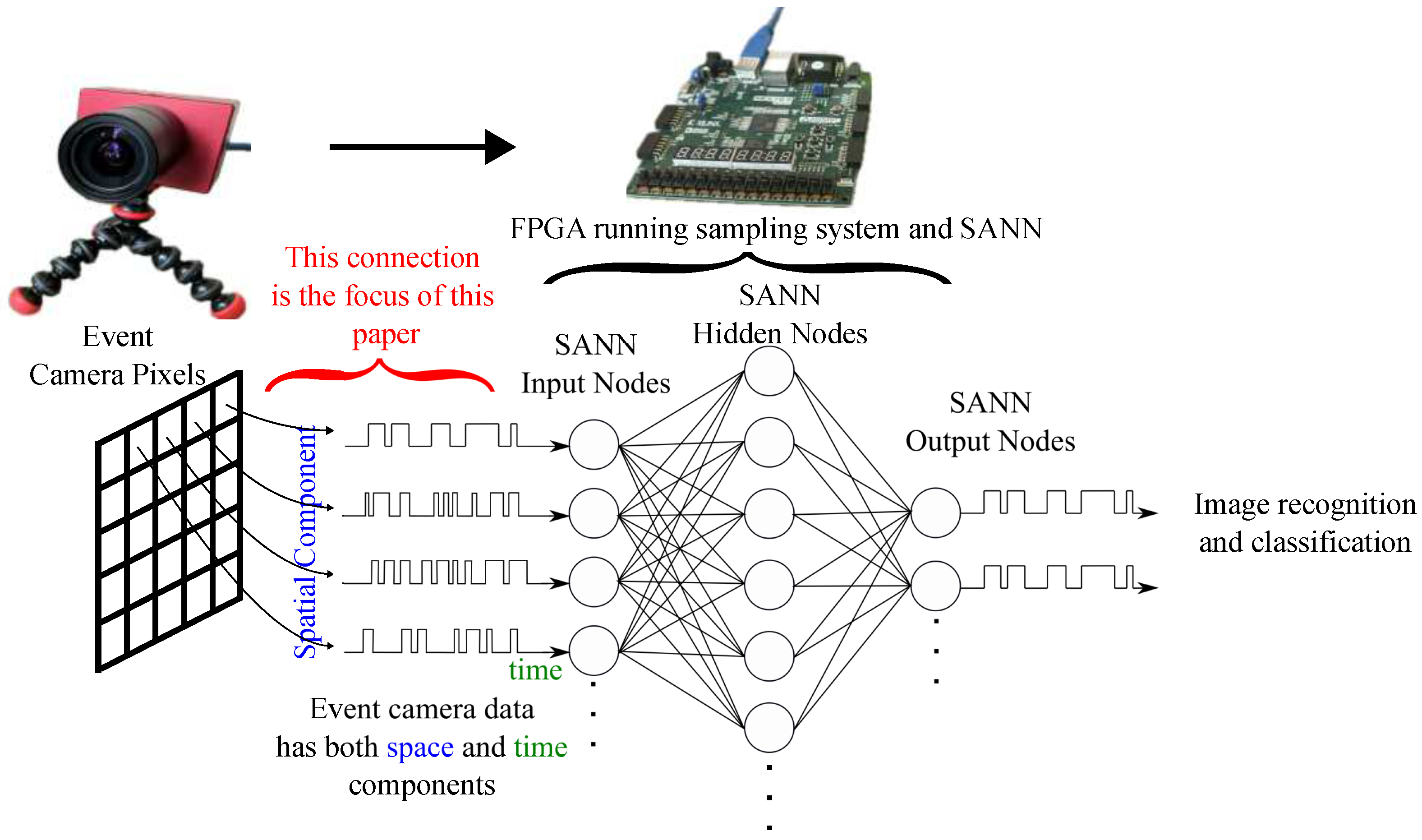
2. System Components

This paper addresses this event camera-to-processor problem in the context of a system performing image recognition. Specifically the system is performing image recognition using a stochastic artificial neural network (SANN) [13,15,22]. Therefore, brief introductions are now given for image recognition, event cameras, stochastic computing, and stochastic artificial neural networks.

2.1. Image Recognition

In the world of artificial intelligence and machine learning, the concept of image recognition often comes to the forefront. According to Zhang et. al, image recognition is defined as “the technology of using [a] computer to process, analyze, and understand the image to identify different patterns of targets or objects” [23]. Image recognition is often performed using neural networks. Traditionally, this image recognition is performed using standard digital images as are produced by a conventional camera, which consist of arrays of fixed numeric values representing the data in the image (such as color or grayscale values). These values are used as input to the neural network, which then classifies the contents of the image based on how it has been trained. This paper presents a method by which neural network-based image recognition can be performed on the output of a fundamentally different type of camera, called an event camera.

2.2. Event Cameras

An event camera such as a DAVIS346 COLOR model, Figure 1, is a camera which, instead of recording the light level and color at each and everypixel, only sends information about pixels that change [1]. It is asynchronous, meaning that it does not update its entire pixel output every clock cycle, but rather outputs data only when it detects movement at specific pixels, and only for those pixels [1]. It is designed to mimic the human eye, which sends “spikes” of data to the brain when new information enters the field of view, but does not continually send all information for unchanging aspects [11]. Movement at any pixel within the camera’s view is captured by creating an “event” at that location: a package of data which includes the x- and y-coordinate of that pixel, the timestamp at which the movement was detected and sometimes the polarity of the event (whether the pixel changed to become lighter or darker). Over time, these events can be accumulated to form a grayscale image of any moving objects in the camera’s view, with the grayscale value of each pixel determined by the frequency of “events” at that pixel over the recording time period [22].

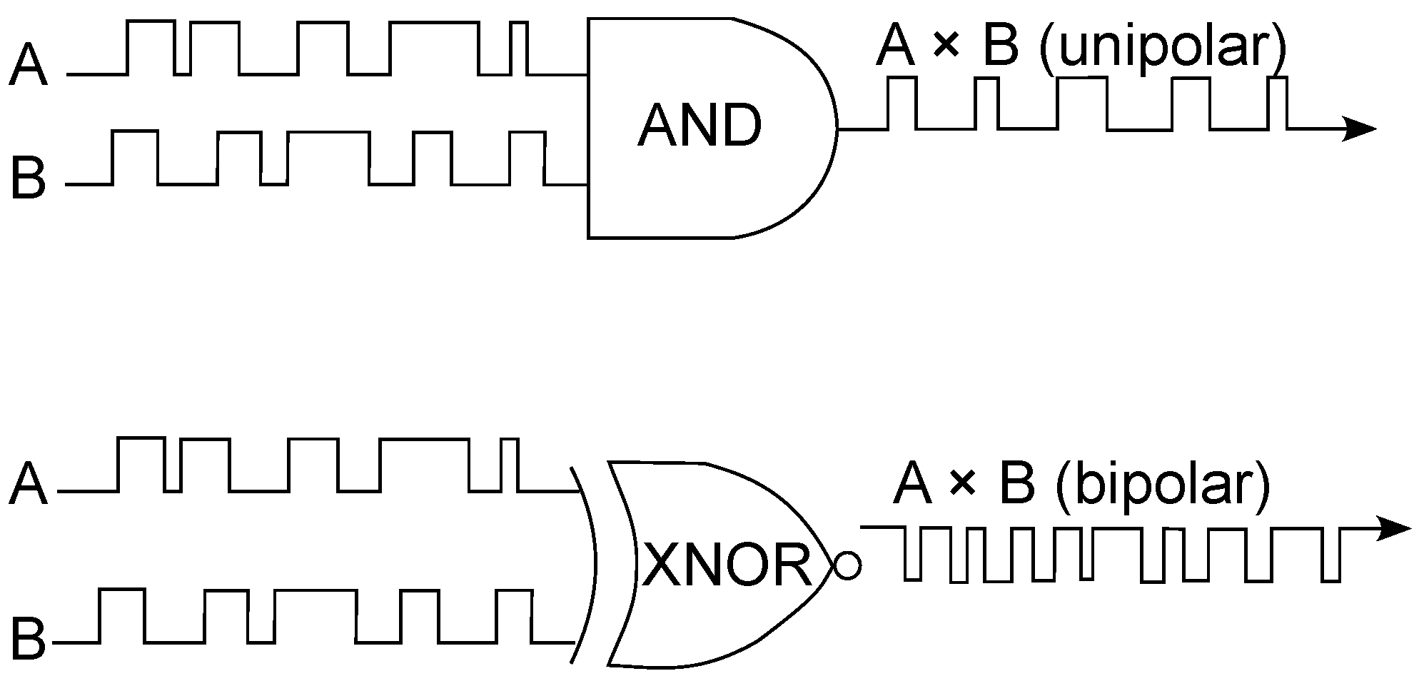
2.3. Stochastic Computing and Stochastic Artificial Neural Networks

The neural network implemented on the FPGA is a stochastic computing artificial neural network, so the next two sections provide a brief background on stochastic computing and stochastic artificial neural networks.

2.3.1. Stochastic Computing

Stochastic computing is an alternative to traditional computing in which values are represented using time-varying bitstreams instead of binary numbers. In traditional computing, all numeric values are represented in binary form. In stochastic computing, numbers are represented as time-varying bistreams with a random distribution of zeros and ones, whose value is considered to be the frequency at which ones occur in the bitstream [14]. This frequency is calculated by dividing the number of ones in a bitstream sequence by the total length of the sequence. For example, a bitstream of length 8 with values “01000001” would be interpreted as having the value 0.25, since there are two ones and a total length of 8. An alternative method of interpreting values is the “bipolar method,” in which values are interpreted as being between −1 and 1, rather than between 0 and 1. This is accomplished by multiplying the ratio of ones by 2 and then subtracting 1. Using the bipolar interpretation, the bitstream “01000001” would be interpreted as −0.5, or 0.25 × 2 − 1 [14]. One advantage of stochastic computing is that operations such as multiplication are much simpler and less resource-intensive, because multiplication of stochastic bitstreams can be accomplished with a single bitwise AND gate (when using unipolar interpretation) or an XNOR gate (when using bipolar interpretation) [14]. This can lead to improved resource usage by the system if much arithmetic is used, and if other stochastic computing components are also implemented in an efficient manner [24,25,26]. Figure 2 shows a diagram of how these logic gates are used to multiply stochastic bitstreams.

2.3.2. Stochastic Artificial Neural Networks

One application of stochastic computing is the stochastic artificial neural network (SANN). Figure 1 shows a simple diagram of a SANN, with representations of stochastic bitstreams going into and out of the network. A SANN follows the same structure as a traditional (binary) artificial neural network, except that it uses stochastic computing methods for all inputs, outputs, and weight values [27]. Inputs are continually streamed into the network and outputs streamed out one bit at a time. The relatively low cost of stochastic multiplication is particularly useful in this application, due to the large number of multiplication operators used by neural networks (used to multiply the weights with their respective connections), and stochastic neural networks could potentially use less hardware and power than traditional neural networks [27].

2.4. Using a SANN with Event Camera Data

Due to the time-varying nature of stochastic computing, it lends itself well to event camera data analysis, as the time-varying value at each camera pixel (with polarity ignored) can be interpreted as a stochastic bitstream, whose value is determined by the frequency of events at that pixel. A pixel at which events (interpreted as ones in a stochastic bitstream) occur frequently would have a higher stochastic value, while a pixel at which events occurred rarely would have a lower stochastic value. Thus, it might be interpreted that a SANN could be useful to perform image recognition on event camera data [22,28]. To accomplish this, each pixel in the event camera’s field of view would need to be interpreted as a stochastic bitstream and converted into a series of zeros and ones. A zero would occur in the bitstream at any timestamp at which no event occurred at the corresponding pixel, and a one would occur at any timestamp at which an event did occur. Each of these bitstreams corresponding to an event camera pixel would be sent as inputs to a SANN, which would perform the image recognition of the data. There would need to be as many inputs to the SANN as there were pixels in the event camera data, although this number could be reduced by pooling and/or cropping the data (this practice is discussed later in this paper).
Due to the functional structure of a SANN (which contains many parallel processes and individual logic gates for multiplying the neural network’s weights with its connections), it was determined that an FPGA would be the best platform on which to implement a SANN. Unlike a CPU, for which each thread can only run instructions in a serial manner, an FPGA can implement parallel logic, limited only by the number of resources on the FPGA itself. It can also implement logic gates on physical hardware rather than generating them through software as would be done if the SANN were implemented on a computer.

2.5. Illustration of Problem Addressed by This Paper

As described in the Introduction, this work involves connecting an FPGA SANN with an event camera where both devices communicate through serial ports. There are likely to be different numbers of events occurring at any given timestamp on the camera. For example, at one timestamp, fifty events could occur, while at the next five could occur, or even zero. Table 2 shows a sample of what a set of event camera data can look like, illustrating how different numbers of events (including zero) can occur at each timestamp. Since at this point the data is not being processed in real time, this would lead to timing irregularities, as it takes more time to send, receive, and process data from fifty events than data from five or zero events. As a SANN is clocked at a regular interval, and would need to be clocked once for every timestamp if all event data is to be processed, this phenomenon presents a challenge as it would be very difficult to synchronize the event camera data with the SANN’s clocking rate.

2.6. Proposed SANN Front-End Architecture

Our solution to the challenge described in Section 2.5 is to create a sampling system, which will set up a regular sampling period at which to clock the SANN. This period will be relatively slow compared to the system clock, to ensure that the program sending event data always has time to send all event camera data corresponding to one timestamp before the end of the SANN system’s sampling period. During each sampling period, exactly one timestamp will be selected, and at the end of the sampling period, all SANN inputs corresponding to sampled events will be set to 1. All other data received during the period not associated with the selected timestamp will be discarded. The stochastic values of the SANN inputs, over time, will equal the frequencies at which events occur at their corresponding pixels, at timestamps which are sampled by the system. The SANN will have an effective clocking rate equal to this user-defined sampling period, and will produce output once every sampling period, and the length of the stochastic bitstream coming from its outputs will be measured in sampling periods.
An additional effect of the nature of the sampling system being designed is that only timestamps at which events occur will factor into the stochastic values input to the SANN. If “gaps” occur between timestamps at which no events occur, these gaps will not factor into the stochastic values. This ensures that the stochastic values associated with the camera’s outputs will not be lessened by any gaps that occur with no events (which can lead to less accuracy in image recognition), and only information associated with actual movement in the camera’s view will be considered. A diagram illustrating the concept is shown in Figure 3. This figure shows how ignoring the time gaps leads to concentration/compression of the event camera data.

3. Materials and Methods

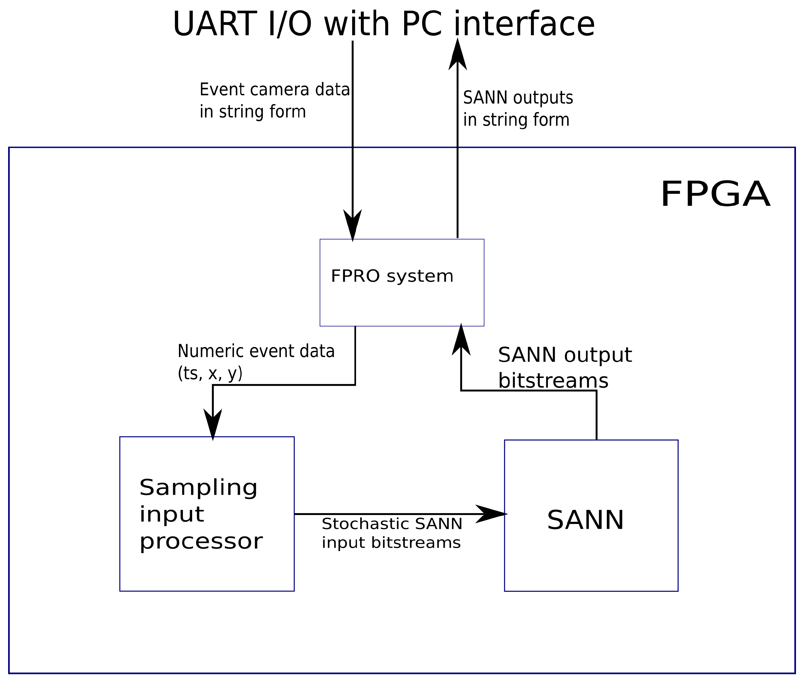
3.1. Background—UART Interface and SANN

Figure 4 illustrates the full system used for this design. It consists of three major subsystems: (1) a subsystem to implement Universal Asynchronous Receiver/Transmitter (UART) Input/Output (I/O) interface with the FPGA, (2) a SANN to perform the image recognition, and (3) the sampling input processor, which is the main focus of this paper. The UART interface was implemented using Xilinx’s MicroBlaze microprocessor [29] and Pong P. Chu’s FPGA Prototyping (FPro) system, a system-on-chip design allowing communication between the MicroBlaze software (version 2022.2) and the FPGA hardware [30]. The FPGA board used in this project was the Digilent Nexys4 DDR prototyping board, which makes use of a Xilinx Artix-7 FPGA [31]. This board was selected because of the board’s availability and the author’s pre-existing experience with the hardware and software. The SANN design used for this project is a sequential, fully-connected neural network that has 256 inputs which represent a 16 × 16 grid of pixels. The SANN had 32 hidden nodes and 10 outputs, one representing each digit in the MNIST dataset (0 through 9) on which the system was trained and tested. The SANN itself and the FPro system will not be discussed in detail, as they are not the primary focus of this paper, however, Figure 4 shows how the three major subsystems interact with each other. The remainder of Section 3 focuses primarily on the event data processor subsystem, i.e., the “Sampling Input Processor” system.

3.2. Overview of the Sampling Input Processor System

Figure 5 shows a flowchart of the next-state logic of the input processor module as a whole, implementing all of the processes described in this section. The sampling input processing system designed for this system, implemented by a SystemVerilog module called “input_processor”, has three major tasks:
  • First, it converts the ASCII character data received through the UART serial port back into numeric representations of the timestamp, x- and y-coordinate, Section 3.2.1.
  • Secondly, it selects one timestamp per T s to sample, Section 3.2.2, and translates the x- and y-coordinates of all events received with that timestamp into SANN input positions, Section 3.2.3.
  • Finally, at the end of each sampling period, it writes 1’s to the SANN input array for each position accumulated from the sampled events, Section 3.2.4.
As is the case for the modules of the SANN itself, the input_processor module uses the enable signal produced by another module (the “en_sig_gen” module [13]) to mark the beginning of sampling periods, although its overall effective clocking is not slowed to T s as is the case for the SANN. Each clock cycle in which this enable signal is equal to 1 marks the beginning of a new sampling period. This signal served to implement a user-defined sampling period, or rate at which data would be sent to the SANN. The length of this period will be referred to as T s from this point forward in this paper, and any time a “sampling period” is referenced, this is what it refers to.
Before describing details of the three major tasks of the sampling input processor system, the details of the system’s input format are described. For ease of use and readability, all input to the sampling input processor system (as well as output from the SANN) were designed to be in character or string form. Input consisted of strings of the form:
“[timestamp]t[x-coordinate]x[y-coordinate]ye”
Such a string represents one single event from an event camera, as shown by a row in Table 2, and is sent to the FPGA’s UART serial port one character (byte) at a time. The first part of the string is a numeric value representing the timestamp at which the event occurred. Next, the letter ‘t’ represents the end of the transmission of the timestamp. Next, the numeric x-coordinate and the stop signal of ‘x’, followed by the numeric y-coordinate and the stop signal ‘y’ are sent. Finally, ‘e’ is sent to mark the end of the transmission of that event. For example, if an event occurred at position (8,14) at timestamp 2104, the string sent to the system via UART would be:
“2104t8x14ye”
Any characters other than digits 0 through 9, ‘t’, ‘x’, ‘y’, and ‘e’ will be ignored if sent to the FPGA. The details of the three major tasks of the sampling input processor system are now described in the following four subsections.
Table 3 shows the Xilinx Artix-7 FPGA utilization of the Sampling Input Processor module. The Block Random Access Memory (BRAM) Blocks are 36Kb RAMB36. The Lookup Tables (LUTs) are 6-input. Each logic slice has 4 LUTs and 8 flip flops (FF) [31].

3.2.1. Translating Event Strings into Numeric Event Data

The first task performed by the input_processor module in Figure 4 is to convert the ASCII character strings received from the UART port into numeric event data. Figure 6 shows a simple representation of how the character data is translated into stochastic SANN inputs by the input processor module. Chu’s UART module [30] was modified to output both the last byte received (called “last_byte_received”) and a signal to alert the main system that new data is available (called “data_received”). Both of these signals are sent as inputs to the input_processor module. When a rising edge is detected on data_received (indicating there is new data which has not been processed yet), the system begins processing the data in last_byte_received. First, it is determined whether or not this byte is a numeric character (0 through 9). If it is, the value is converted from character to unsigned integer form (equal to the numeral represented by the character) and stored to a register called “input_buf_reg.” This register is used as an input buffer to properly assemble data from the individual bytes from UART. As numbers are sent into the system in character form, digit by digit, the next-state value for input_buf_reg is multiplied by 10 and added to the newly received digit (after converting from character to integer) and re-written to input_buf_reg. This serves to shift the existing decimal digits left by one, and add the new digit as a least significant value (ones place). This process continues until a non-numeric character is received. To accommodate the extremely large timestamp values sometimes produced by a real event camera, 64 bits were used for input_buf_reg.
When a non-numeric character is received, what happens next depends on the value of this character. If it is anything other than ‘t’, ‘x’, ‘y’, or ‘e’, then nothing will happen, the character will be ignored and not stored anywhere (although input_buf_reg will still be zeroed out). If ‘t’ is received, the value currently in input_buf_reg will be written to a second buffer register called “ts_buf_reg.” This serves to hold the newly received timestamp value until all other data associated with that event (the positional coordinates) have been received.
If ‘x’ is received, input_buf_reg’s contents will be written to a buffer register to temporarily store the x-coordinate, called “x_buf_reg”, and if ‘y’ is received, input_buf_reg’s contents will be written to a buffer register for the y-coordinate called “y_buf_reg”. After any of these signals are received and input_buf_reg’s contents are written to the appropriate place, input_buf_reg is then zeroed out to be ready for the next numeric data. The reason additional buffer registers are used to store the values for timestamp, x-coordinate and y-coordinate while the event string is being processed is so that all three of these values can be written to their final registers at the same time when the full event string has finished being processed.
When ‘e’ is received, indicating the end of transmission of an event, the three buffer registers holding the event data (ts_buf_reg, x_buf_reg, and y_buf_reg) will be written to the main registers corresponding to these pieces of data, which are called ts_reg, x_reg, and y_reg respectively. These registers contain the numeric event data to be used by the system. After these three registers have been updated, the three event data buffer registers are zeroed out to be ready for processing a new event string.
Table 4 shows the results of each step of this process, when the event string “2104t8x13ye” (representing an event at timestamp 2104, at position (8,13)) is sent to the system one character (byte) at a time. Each row of the table shows the contents of the relevant registers after each individual character is received.

3.2.2. Sampling Events at Selected Timestamps

The second task performed by the input_processor module was to select a timestamp to sample during each sampling period (time interval of T s ), and collect the events which occur at that timestamp. All events at one timestamp per sampling period are selected to be translated into SANN inputs during this task. As event strings are sent continually to the system and T s is set by the user such that it is guaranteed to be possible to receive all events at the sampled timestamp, there will always be sampled event data to translate to SANN inputs at the end of each sampling period.
The value of the timestamp at which events are to be sampled is stored in a register called “sampled_timestamp”. To start the sampling process, first this register (sampled_timestamp) is set to zero at the beginning of the sampling period (when the enable signal “en” is equal to 1). This ensures that the timestamp sampled during the previous period will not be sampled again. After a full event has been received (when the character ‘e’ is sent to the input_processor module’s input from UART), it is determined whether or not the timestamp of the newly received event represents the first new timestamp received after the beginning of the current sampling period. This is done by checking whether the value in sampled_timestamp is zero (indicating that a timestamp has not yet been sampled during this period) and if it is, comparing the value in the timestamp buffer register of the new event to the value in ts_reg (the timestamp of the previously received event). If this condition is met, then the new timestamp will be sampled, and its value is then written to sampled_timestamp. A one-bit signal called “new_timestamp” is assigned to be 1 when when sampled_timestamp is nonzero and equal to the contents of ts_reg, and zero otherwise. This signal being equal to 1 indicates to the system that the event whose data is currently in ts_reg, x_reg and y_reg is to be sampled, and that the coordinates of this event should be converted into SANN inputs. The data associated with events not being sampled will simply be overwritten when the next event arrives, and will not be converted into SANN inputs.

3.2.3. Translating Event Data to SANN Input Positions

Once the three pieces of event data (timestamp, x-coordinate, y-coordinate) have been written to their respective final registers (ts_reg, x_reg, and y_reg), they still need to be translated into SANN inputs. Due to the sampling nature of the system, however, only the events that occur at the timestamp contained in the register sampled_timestamp will be translated. As mentioned earlier, the signal new_timestamp marks when this condition is true. When new_timestamp is equal to 1, another buffer register, equal in size to the SANN input register (256 bits in this case), is used to store the SANN input locations which are to be set to 1. This register is called sann_inputs_buf_reg. While new_timestamp is 1, the contents of the x- and y-coordinate registers (x_reg and y_reg) are used to determine which locations in this array should be set to 1. The SANN input array represents a linearized version of a square array of event camera pixels. For a n × n array of pixels, the SANN input array would be n 2 bits long (which is why this system, which is based on a 16 × 16 input array, has a 256-bit input array). The position in this linearized pixel array corresponding to an event received at position (x,y) would be at position ( ( x 1 ) × n + y ) 1 (assuming that the received coordinates index from 1 and Verilog’s arrays index from 0, as is the case in this design). This position of sann_inputs_buf_reg to be set to 1 is determined by substituting the contents of x_reg and y_reg into this formula, and is stored as a 10-bit value called input_ndx. This will occur for every event received with the timestamp to be sampled.

3.2.4. Update the SANN Input Array

At the beginning of each sampling period, the output register sann_inputs is updated by OR’ing its contents with sann_inputs_buf_reg. This sets all positions in sann_inputs to 1 for which the corresponding value in sann_inputs_buf_reg is 1, without zeroing out any elements in sann_inputs. The only time elements in sann_inputs are zeroed out is when their hold time has passed, which is discussed in the next paragraph. The register sann_inputs is passed as an output to input_processor, where it connects directly to the 256-bit input of the SANN. Thus, the SANN’s inputs are only updated at a rate of T s , corresponding to the SANN’s effective clocking rate.
Figure 7 shows a timeline of the sampling process described above, indicating when events at several consecutive timestamps are received by the system. Table 5 describes what is happening at each point on the timeline in Figure 7 and actions taken by the sampling input system at each of these points. It is important to note that the numbers on the timestamp labels (Time Stamp 1, Time Stamp 2, etc) do not necessarily refer to actual consecutive timestamp numbers separated by one, but simply to differing timestamps in the order in which they are sent to the FPGA. There could be a larger real time gap between them than 1, and this gap would not be taken into account.

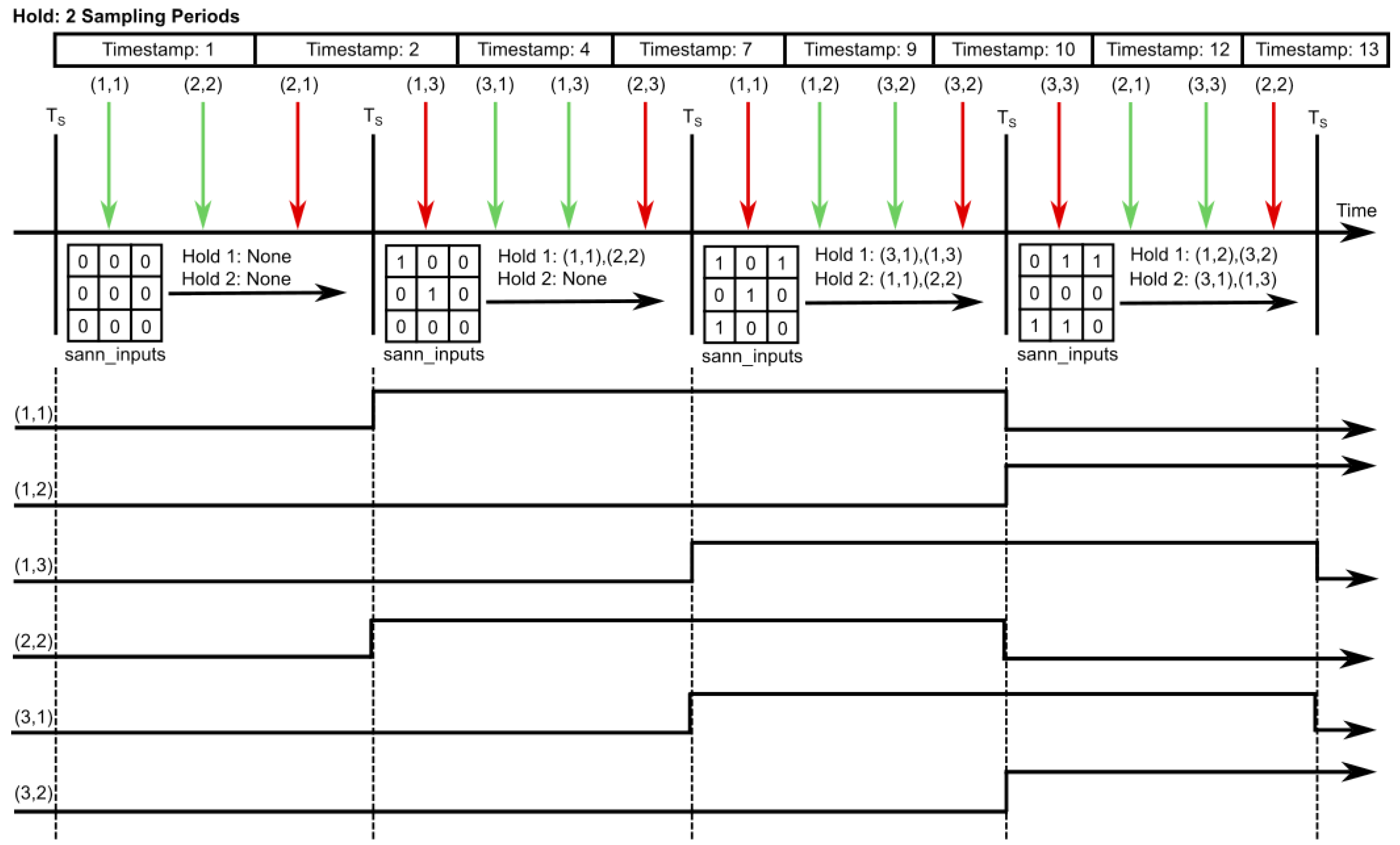
3.3. Hold Functionality
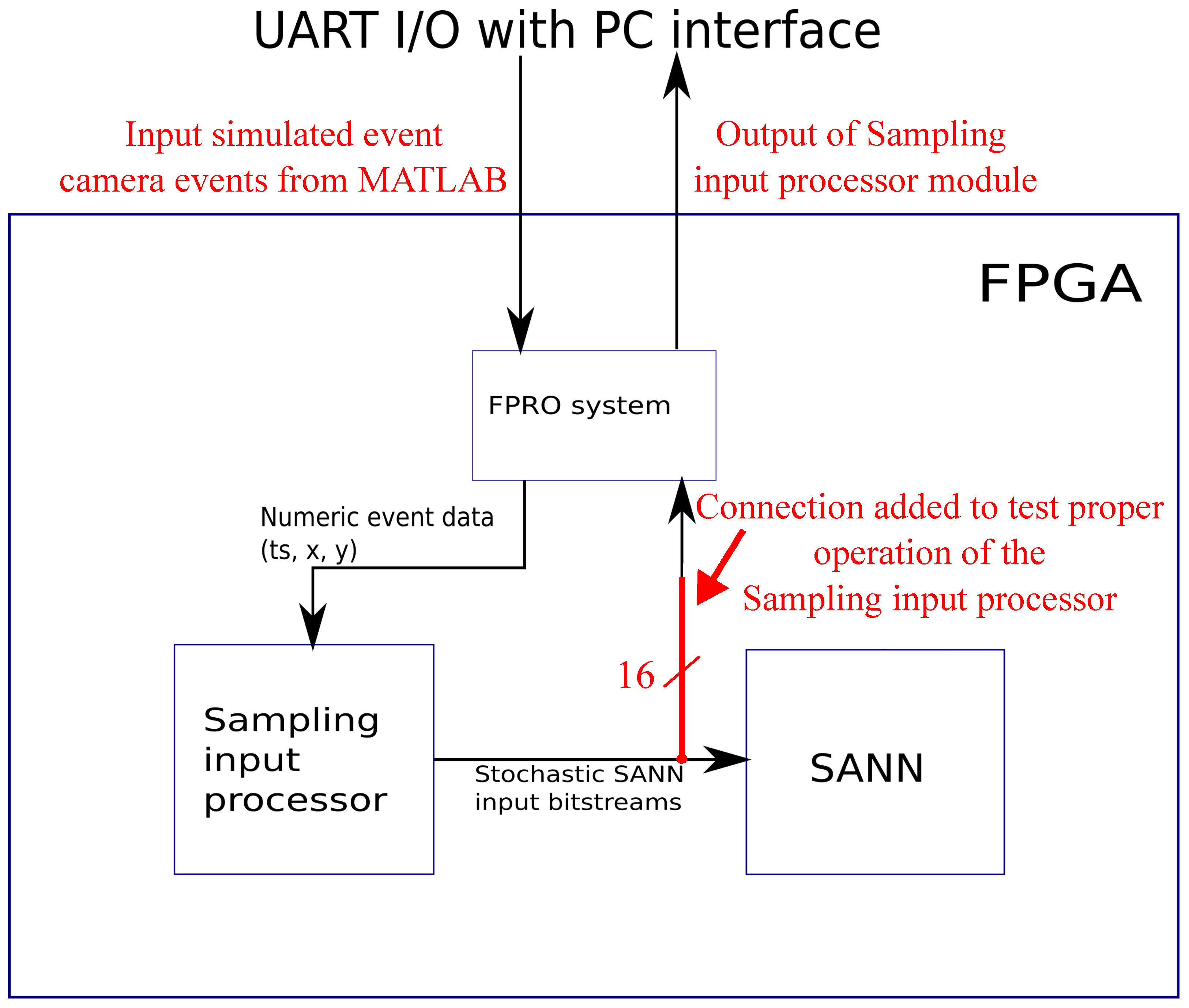
Another feature of this design related to the input system is the hold functionality, which is illustrated in [13,15,22] and in Figure 8. Since the stochastic pixel values from a real event camera are often extremely sparse (low event frequencies at each pixel), a “hold” can be used to artificially increase the stochastic value of each input for more accurate image processing. The way this works is by specifying a hold period, and each time a SANN input position is set to 1 (representing an event at the corresponding pixel), it is “held” at 1 for as many sampling periods as is specified by the hold period value. For example, with a hold period of 2, each pixel at which an event occurred would be held at 1 for two sampling periods after the event occurred, rather than for only one sampling period if no hold were used. This functionality is implemented using a counter which increments by 1 at each sampling period, and a set of registers, one corresponding to each input, in which the time at which the last event occurred for that input position is saved. Once the difference between the current system counter and the value in each “hold status” register reaches a value greater than the hold period, the corresponding SANN input value is set back to zero. The hold value is set by the user, and to run the system without a hold the hold value should be set to 1.

4. Test Setup

The sampling input system, implemented with the input_processor module, was primarily tested first using Verilog’s debugger utility, and later by writing a special synthesizable top-level module called “input_processor_test”, designed specifically to test it. For the former, the sampling period was purposely set to be very slow (more than 10 s), and an input event string was manually sent to the UART port via a PuTTY terminal. PuTTY is a program which allows direct manual communication with a serial port from a computer. After each character of the string was sent, the debugger window was viewed to ensure the buffer registers and event data registers had the proper values in them. These registers were observed up until the passing of the hold period to ensure that they held their values until that point and were zeroed out when the hold period passed. The signals related to determining which timestamp should be sampled were also viewed and debugged in this manner.
A MATLAB script was written to continually send event strings to the FPGA with this module programmed to it, and to read the FPGA’s UART output whenever output was available (once per sampling period T s ). Figure 9 shows a block diagram of the system used to test the Sampling Input Processor.
Over time, the value of the FPGA’s outputs (corresponding to the input_processor_test module’s outputs) were accumulated and interpreted as stochastic numbers [15]. Each of the 16 outputs was calculated according to (1).
output   of   sampling   input   processor = n = 1 N u m _ o f _ T s _ P e r i o d s b i t _ v a l u e n N u m _ o f _ T s _ P e r i o d s
As the input_processor module’s job was to convert from event strings to stochastic numbers, the stochastic values of the module’s outputs should ideally equal the frequency of events at each position being sent to the FPGA. The MATLAB script compared these values calculated by (1) to the event frequencies being sent to ensure that the module was producing the correct values. The event frequencies being sent were calculated according to (2).
input   freqencies   with   time   gaps = n = 1 ( l a s t _ t i m e s t a m p f i r s t _ t i m e s t a m p ) b i t _ v a l u e n ( l a s t _ t i m e s t a m p f i r s t _ t i m e s t a m p )
A phenomenon initially perceived to be a challenge (i.e. problem) arose with very sparse event data, in which timestamps between consecutive events could have “gaps” between them at which no events occurred, as shown by the last three timestamps in Table 2. Since no data existed in the event data file for time instants at which no events occurred, these gaps could not be sampled by the system, which would simply “skip” to the next timestamp at which an event did occur (see Figure 3). This leads to higher stochastic values being read for the inputs than the actual event frequencies in the input data. This non-sparse data also changes the concept of a hold. Figure 10 depicts the concept of a hold with sparse data. It can be compared to Figure 8. The MATLAB script compared the ouput values calculated by (1) to the event frequencies being sent with time gaps ignored. The event frequencies being sent with gaps ignored were calculated according to (3).
input   freqencies   ignoring   time   gaps = n = 1 ( l a s t _ t i m e s t a m p f i r s t _ t i m e s t a m p ) b i t _ v a l u e n N u m b e r _ o f _ u n i q u e _ t i m e _ s t a m p s

5. FPGA Hardware Results

Three FPGA hardware Unit Tests were performed to demonstrate performance. They are described in the following sub-sections. Figure 11 shows the unit test results of testing a 16-input instance of the Sampling Input Processor Module, performed on the FPGA and running a MATLAB script to send data to and read values from the board. A sampling period of T s = 24 milliseconds and bitstream length of 20,000 sampling periods was used for all of the tests.
To asses the performance, the stochastic outputs of the input processor module received from the FPGA are plotted alongside two interpretations of the event frequencies being sent to the FPGA: (1) the frequencies with time gaps taken into account (green bars), and (2) the frequencies with time gaps ignored (blue bars). These correspond to (2) and (3), respectively. The values of the red bars representing the output from the FPGA were calculated according to (1).

5.1. Unit Test 1 of Sampling Input Processor Module: Non-Sparse Input and No Hold

For the first test, the input processor was instantiated with no hold (accomplished by setting its hold parameter to 1). A set of input data was created by generating 16 values between 0 and 1 and converting these values to a series of simulated camera events, using MATLAB, with the frequency of events at each of the simulated 16 pixels being equal to its corresponding random value between 0 and 1. These simulated events were sent to the input processor module through the UART port, and the module’s outputs were sent directly through the UART port to be read in MATLAB. The results of this test are shown in Figure 11a. It can be seen that the input processor module’s stochastic outputs from the FPGA closely match the actual event frequencies being sent to the FPGA. This is shown by the red and green bars being approximately the same.

5.2. Unit Test 2 of Sampling Input Processor Module: Sparse Input and No Hold

For the next test, the same setup was used except the input values were divided by 20 before converting them into event form. This served to create sparse simulated event data which contained time gaps. The results of this test can be seen in Figure 11b. As with Unit Test 1, the stochastic outputs of the input processor module received from the FPGA are plotted alongside two interpretations of the event frequencies being sent to the FPGA: the frequencies with time gaps taken into account, and the frequencies with time gaps ignored. It can be seen that the outputs of the input_processor module closely match the latter rather than the former, which is as expected. Note the change in y-axis scaling, when compared to Figure 11a.

5.3. Unit Test 3 of Sampling Input Processor Module: Sparse Input and Hold of 2

For the last test, the same setup was used as in the second test (with the sparse data) but the input processor was implemented with a hold value of 2. The results of this test can be seen in Figure 11c. Note that the outputs of the input processor module are roughly double that of the input event frequencies with time gaps removed.

6. Analysis, Discussion, and Supplemental FPGA Results

In this section analysis will be shown regarding data sparsity, time convergence, normalization, repeatability, range, and some initial characteristics of the hold system.

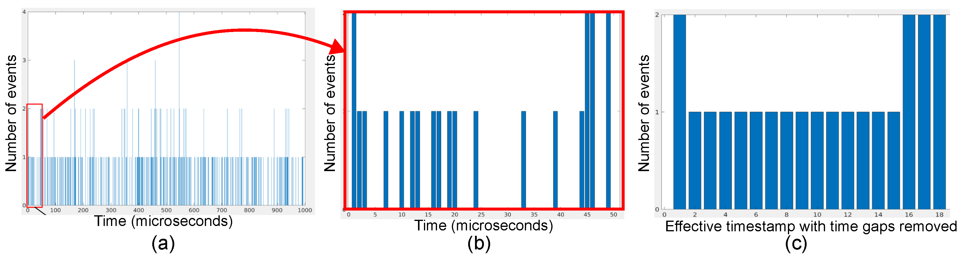
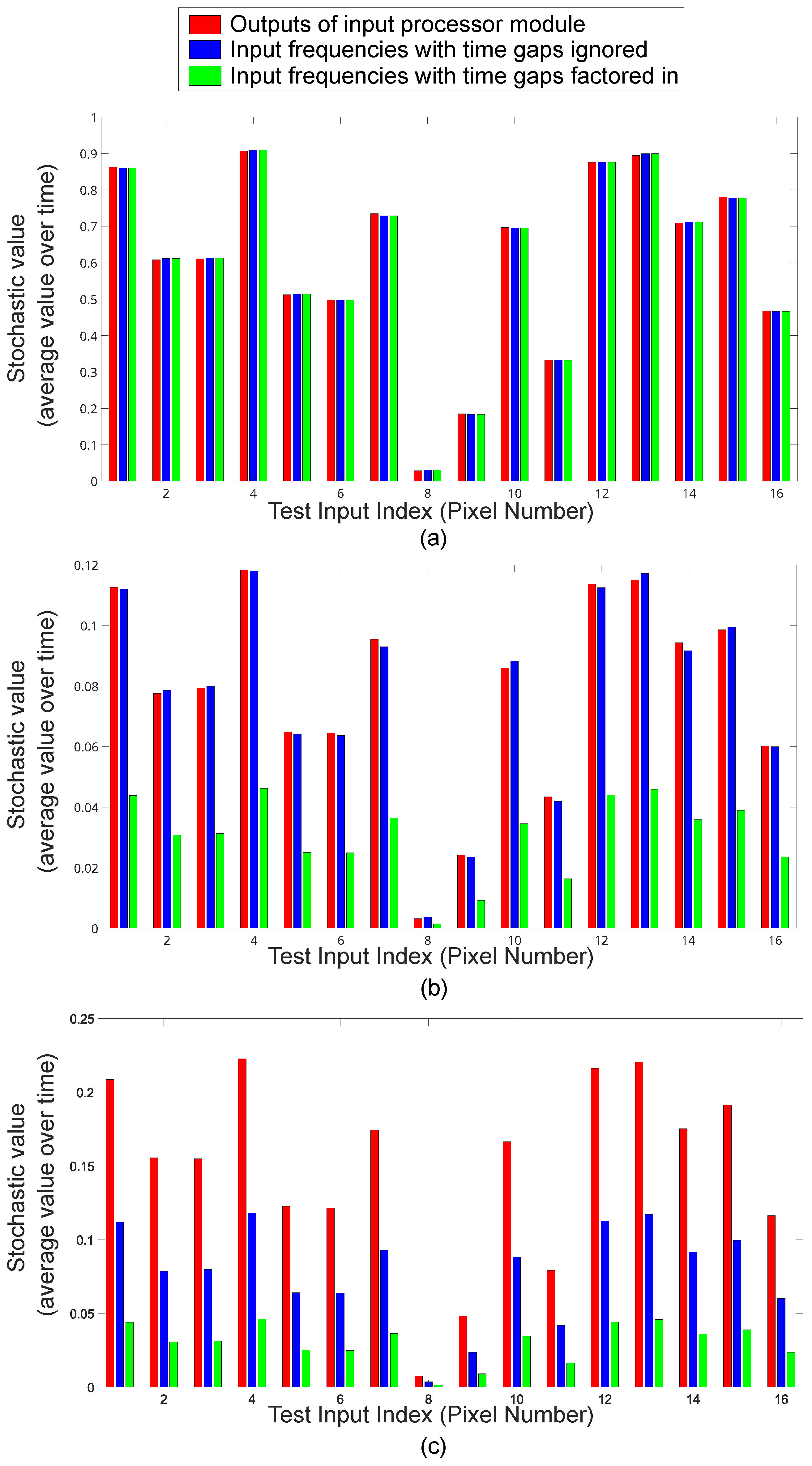
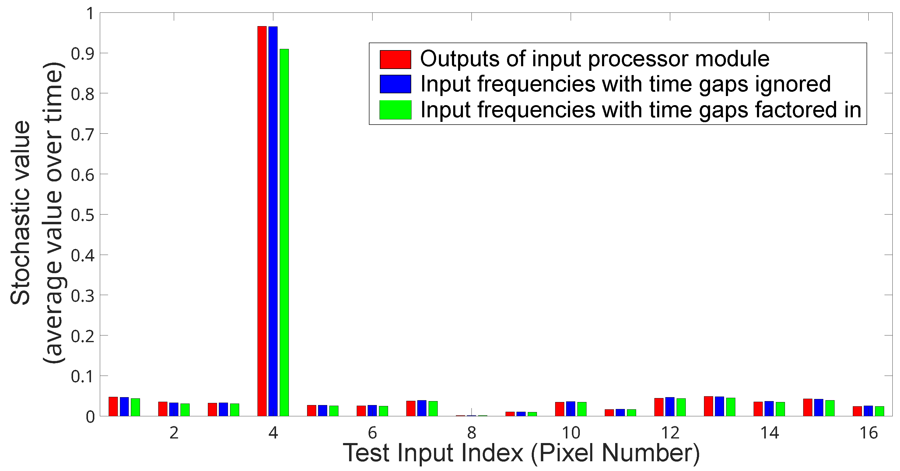
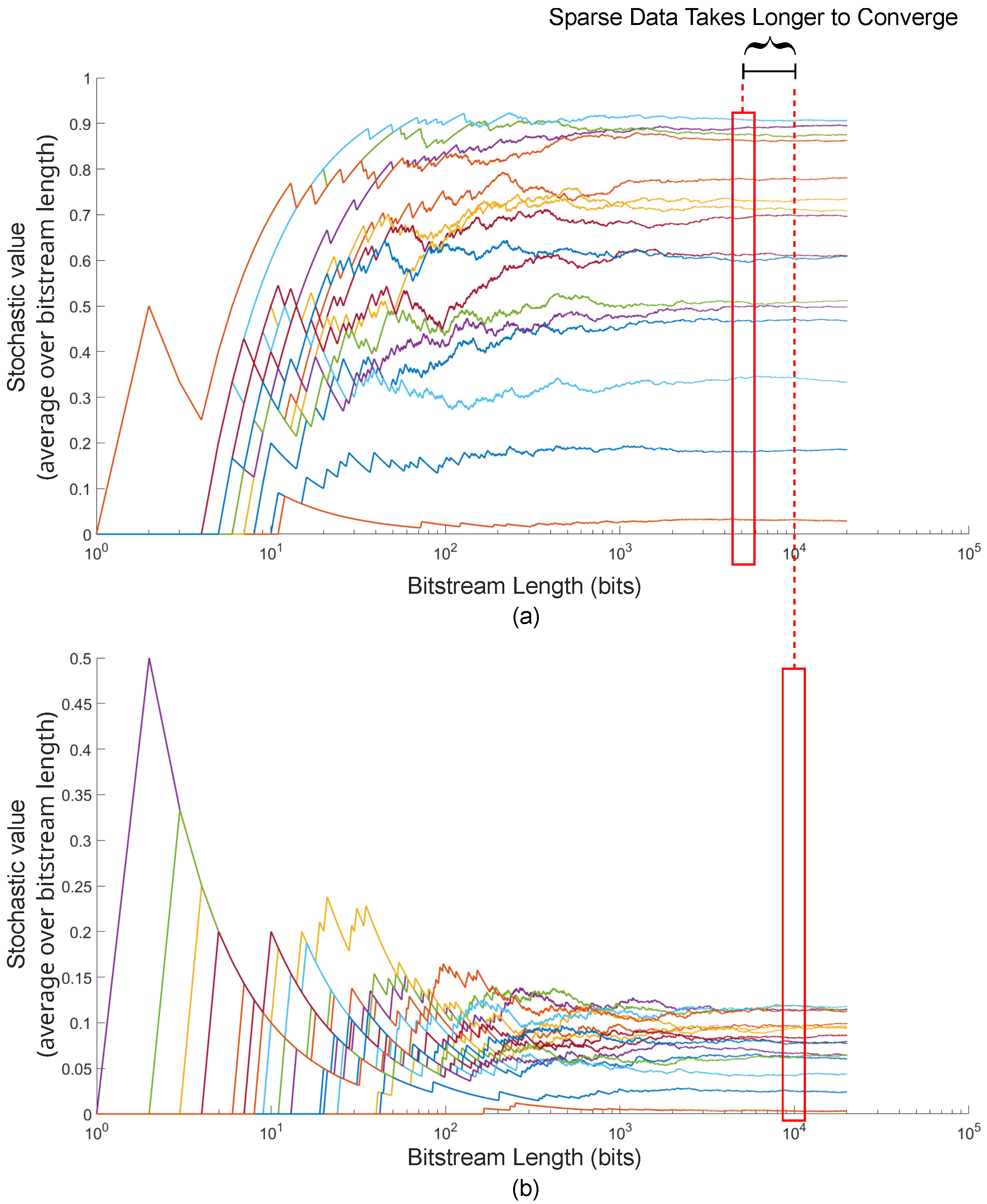
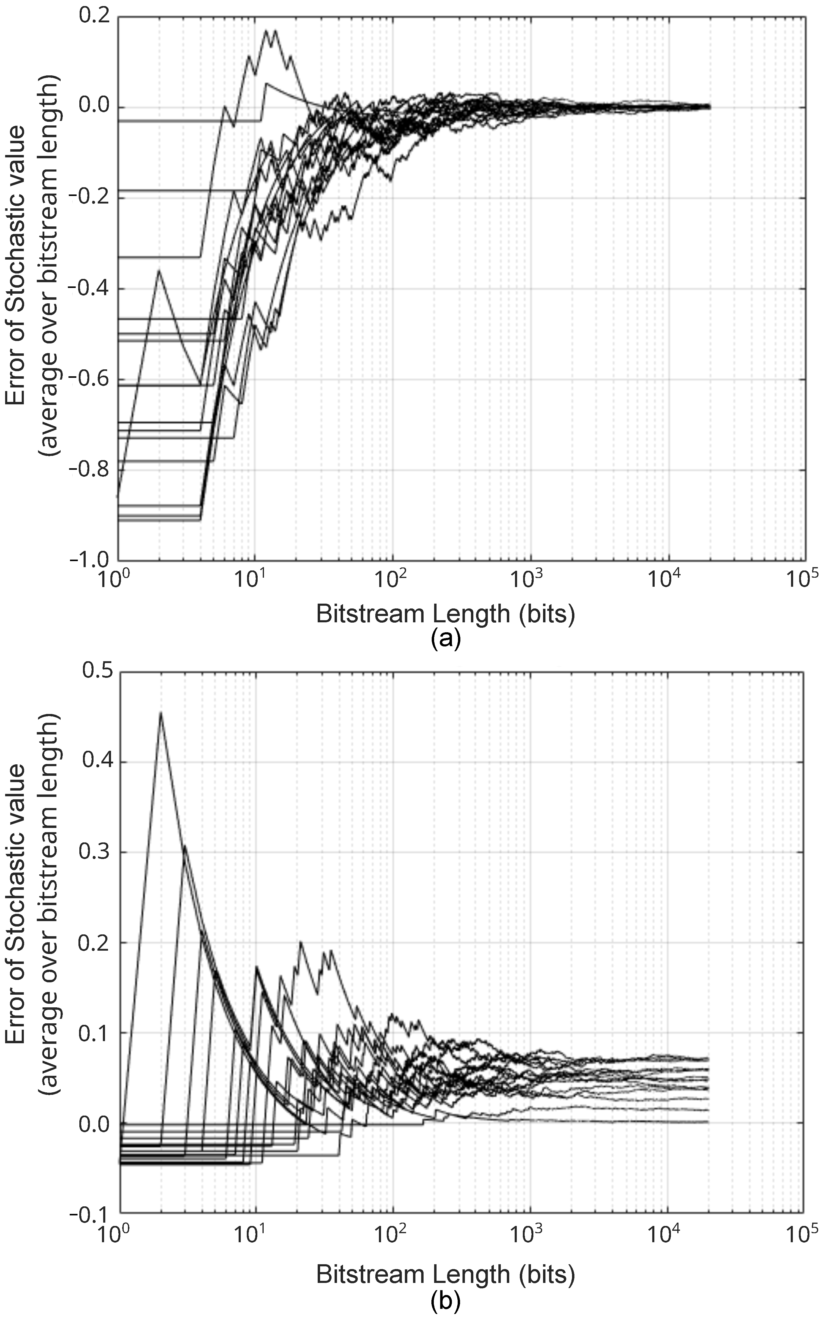
6.1. Sparse Data Analysis

Prima facie, looking at Figure 11b, one may be inclined to conclude that because the green bars diverge from the others when processing sparse data, then the output processor must always overestimate sparse values. However, Figure 11a, showed that sparse data could be accurately represented by the input processor. This is shown by the red and green bars being approximately the same for sparse input 8. So, one may ask: “If the input processor was able to accurately output values of approximately 0.03 in Figure 11a, why did it over estimate sparse values shown in Figure 11b (see, for example, inputs 2 and 3 which are also approximately 0.03)?” The reason is because the input values in Figure 11b are all sparse, but this is not the case for the input values in Figure 11a. The non-sparse inputs in Figure 11a increased the number of unique time stamps. This value is in the denominator of the equation developed to estimate the input processor’s output value (3). The increased value of “Number_of_unique_time_stamps” resulted in a more accurate averaging. A follow-on experiment was performed to provide evidence of this analysis. In this follow-on experiment, all the input values except one were sparse. The hardware experiment data is shown in Figure 12. In these results, as predicted, the red and green bars are similar as in Figure 11a, and unlike the sparse data results in Figure 11b.

6.2. Convergence Time Analysis

Analysis was performed to evaluate the FPGA hardware output data convergence times for the sampling input processor data, Figure 13. This time-series data corresponds to the data in Figure 11. The Figure 11 data was sampled at bit stream length 20,000 which is when all data has had a chance to converge to steady-state values. Figure 13 shows how the output changes with increasing bitstream length. As expected with stochastic systems, sparse data takes longer to converge. The respective output errors for each signal is shown in Figure 14. This shows how the accuracy/error of the data in Figure 13 changes with increasing bitstream length.

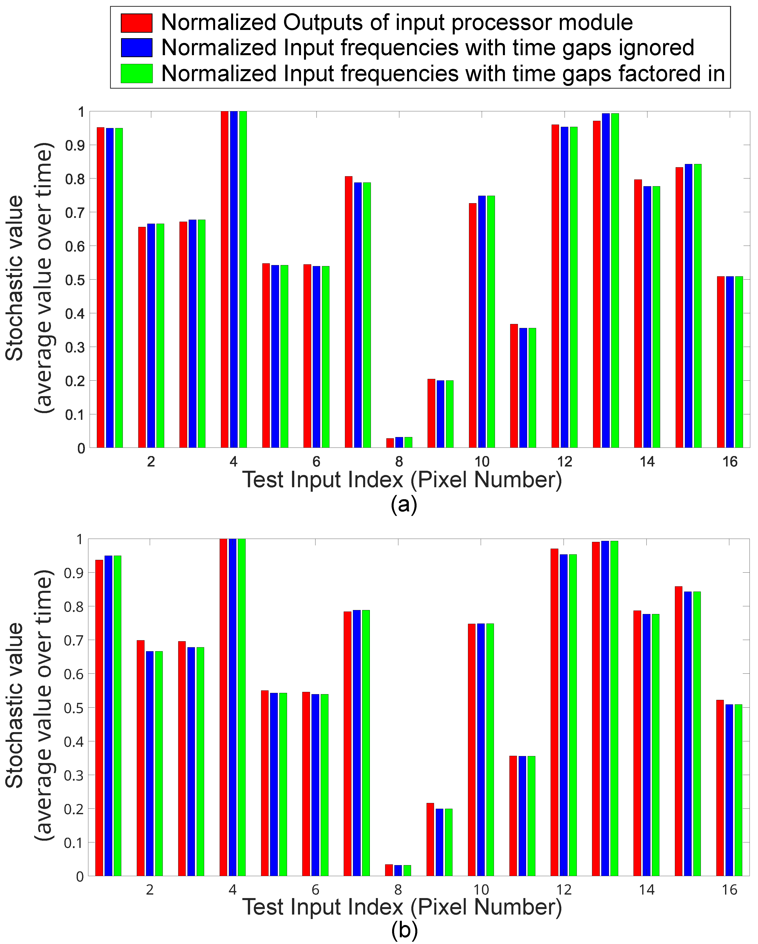
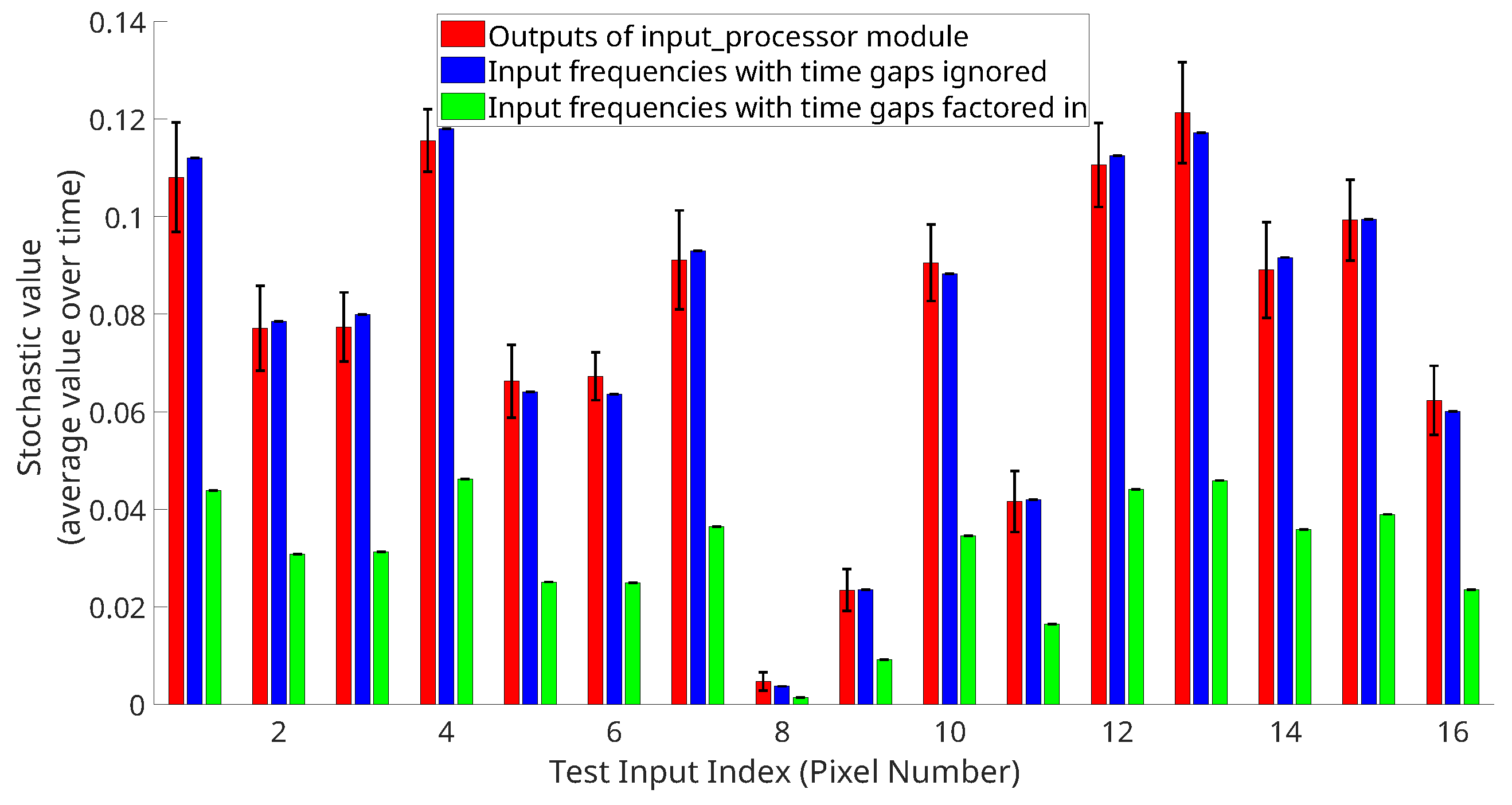
6.3. Normalized Data Analysis

Figure 11b,c show that the absolute values of the input numbers are not maintained by the input processor when all inputs are sparse and when using a hold, however, the relative differences between each color bar’s values are maintained. Figure 15 shows an example of plotting normalized Figure 11b,c data where all red bar data are divided by the max red bar value and plotted, all green bar data are divided by the max green bar value and plotted, and all blue bar data are divided by the max blue bar value and plotted.

6.4. Repeatability Analysis

The repeatability of the system is shown in Figure 16. The same sixteen input values were sent to the FPGA 40 times and the results were recorded. The mean of all 40 runs is plotted as the bar height for each input. The error bars represent +− one standard deviation of the data. This shows the repeatability of the FPGA input processor system. The bitstream data length for each of the 40 runs was 1000. Based on the data in Figure 13, one could expect the error bars to get smaller if a longer bitstream was used for analysis.

6.5. Range of Input Value Analysis

A test of using a uniformly spaced set of inputs from small to large was also performed. This tested that the Sampling Input Processor can operate over a large range. The data is shown in Figure 17. The results are consistent with the rest of the analysis.

6.6. Hold System Analysis

Finally, the hold system is shown to effectively decrease the sparsity of the data. This is shown because the red bars in Figure 11c are approximately double the blue bars in Figure 11c. This is also shown by comparing the red and blue bars in Figure 17c. Figure 18, shows some additional analysis of the data in Figure 17c. The x-axis is not the input index, but is instead the true value input into the Matlab event simulator. A linear curve fit (dashed line) was performed for each of the three colors of data. The slopes are recorded in the legend. The slope of the red line divided by the slope of the blue line is 1.8404. This is an initial analysis, and further investigation is warranted. Additional analysis on the hold can be found in [15].

7. Conclusions and Future Directions

Based on the results of the FPGA input processor analysis, we conclude that it has the potential to be an effective method of processing event camera data for stochastic processing systems.
At the moment, the system is designed to take in simulated event camera data and send it to the FPGA through a computer program such as MATLAB. However, in the future it would be ideal to establish a direct connection between an event camera and the FPGA running the sampling SANN system. This may involve implementing pre-processing logic or software on the FPGA to perform a pooling operation to match camera pixels to SANN inputs. In such a scenario, a much shorter sampling period could be used due to the fact that the camera outputs data much faster than MATLAB could process and send it. This would lead to much faster results from the SANN.
One change which will likely be useful in the future would be to use a larger FPGA with more logic resources on which to implement the system. The Digilent Nexys4 has rather limited space, only allowing for approximately 16 × 16 inputs and 32 hidden nodes, and limited stochastic number generator (SNG) sequence length. Using a larger FPGA could allow for larger input size (such as 32 × 32, which would allow for more detail in images), and/or more hidden nodes and longer SNG sequence length, which could potentially result in greater system accuracy.
One possible drawback of the current sampling system is that, depending on the sampling period length, a lot of potentially useful data can be discarded which could lead to sub-optimal efficiency. This is due to the fact that events at only one timestamp are sampled per period, discarding all other data received during that period. One potential alternative to this method could be to sample multiple timestamps per period, or even sample all events received during a period and simultaneously write them to the SANN inputs at the end of each period. This would serve to further concentrate the event data, as events from multiple timestamps would be treated as if they were from one timestamp. If such a system were implemented, it could potentially replace the hold functionality in the current system. With the proper sampling period length, the accumulation of events over a period being simultaneously written to the SANN inputs at the end of the period would serve to counteract sparsity in the event data without using a hold. Note that this method is essentially a form of quantity-based frame accumulation, which was discussed in Table 1. Future work could also include continuing to optimize the hold functionality [15].

Author Contributions

Conceptualization, S.S., E.C., J.D. and S.K.; methodology, S.S., N.J. and S.K.; software, S.S. and N.J.; validation, S.S., S.K. and N.J.; resources, S.K.; data curation, S.S., N.J., J.D. and S.K.; writing—original draft preparation, S.S.; writing—review and editing, S.S., N.J., E.C., J.D. and S.K.; visualization, S.S., N.J., J.D. and S.K.; supervision, E.C., J.D. and S.K.; project administration, S.K., E.C. and J.D.; funding acquisition, S.K. All authors have read and agreed to the published version of the manuscript.

Funding

This study is supported in whole or in part by funds from the Naval Engineering Education Consortium (NEEC).

Data Availability Statement

The original contributions presented in this study are included in the article. Further inquiries can be directed to the corresponding author.

Conflicts of Interest

The authors declare no conflicts of interest.

Abbreviations

The following abbreviations are used in this manuscript:
AERAddress-event representation
BRAMBlock Random Access Memory
CNNconvolutional neural network
FFFlip Flop
FPGAField Programmable Gate Array
FPro SystemFPGA Prototyping System
I/OInput/Output
LUTLookup Table
NNneural network
RAMRandom Access Memory
SANNStochastic Neural Network
SNGStochastic Number Generator
UARTUniversal Asynchronous Receiver/Transmitter
XNORexclusive NOR

References

  1. Gallego, G.; Delbrück, T.; Orchard, G.; Bartolozzi, C.; Taba, B.; Censi, A.; Leutenegger, S.; Davison, A.J.; Conradt, J.; Daniilidis, K.; et al. Event-Based Vision: A Survey. IEEE Trans. Pattern Anal. Mach. Intell. 2022, 44, 154–180. [Google Scholar] [CrossRef] [PubMed]
  2. Afshar, S.; Nicholson, A.P.; van Schaik, A.; Cohen, G. Event-Based Object Detection and Tracking for Space Situational Awareness. IEEE Sens. J. 2020, 20, 15117–15132. [Google Scholar] [CrossRef]
  3. Monforte, M.; Gava, L.; Iacono, M.; Glover, A.; Bartolozzi, C. Fast Trajectory End-Point Prediction with Event Cameras for Reactive Robot Control. In Proceedings of the 2023 IEEE/CVF Conference on Computer Vision and Pattern Recognition Workshops (CVPRW), Vancouver, BC, Canada, 17–24 June 2023; pp. 4036–4044. [Google Scholar] [CrossRef]
  4. Maqueda, A.I.; Loquercio, A.; Gallego, G.; García, N.; Scaramuzza, D. Event-Based Vision Meets Deep Learning on Steering Prediction for Self-Driving Cars. In Proceedings of the 2018 IEEE/CVF Conference on Computer Vision and Pattern Recognition, Salt Lake City, UT, USA, 18–23 June 2018; pp. 5419–5427. [Google Scholar] [CrossRef]
  5. Mitrokhin, A.; Fermüller, C.; Parameshwara, C.; Aloimonos, Y. Event-Based Moving Object Detection and Tracking. In Proceedings of the 2018 IEEE/RSJ International Conference on Intelligent Robots and Systems (IROS), Madrid, Spain, 1–5 October 2018; pp. 1–9. [Google Scholar] [CrossRef]
  6. Lagorce, X.; Meyer, C.; Ieng, S.H.; Filliat, D.; Benosman, R. Asynchronous Event-Based Multikernel Algorithm for High-Speed Visual Features Tracking. IEEE Trans. Neural Netw. Learn. Syst. 2015, 26, 1710–1720. [Google Scholar] [CrossRef] [PubMed]
  7. Gehrig, D.; Scaramuzza, D. Low-latency automotive vision with event cameras. Nature 2024, 629, 1034–1040. [Google Scholar] [CrossRef] [PubMed]
  8. Liu, B.; Su, M.; Zhang, Z.; Sun, L.; Yu, Y.; Qiu, W. A Novel Coded Excitation Imaging Platform for Ultra-High Frequency (>100 MHz) Ultrasound Applications. IEEE Trans. Biomed. Eng. 2025, 72, 1298–1305. [Google Scholar] [CrossRef] [PubMed]
  9. Fernandez-Rodriguez, L.E.; Rodriguez-Resendiz, J.; Martinez-Hernandez, M.A. An open-source FPGA-based control and data acquisition hardware platform. In Proceedings of the 2021 XVII International Engineering Congress (CONIIN), Queretaro, Mexico, 14–18 June 2021; pp. 1–11. [Google Scholar] [CrossRef]
  10. Vaithianathan, M.; Udkar, S.; Roy, D.; Reddy, M.; Rajasekaran, S. FPGA-Based Motor Control Systems for Industrial Automation. In Proceedings of the 2024 International Conference on Sustainable Communication Networks and Application (ICSCNA), Theni, India, 11–13 December 2024; pp. 249–254. [Google Scholar] [CrossRef]
  11. Lichtsteiner, P.; Posch, C.; Delbruck, T. A 128× 128 120 dB 15 μs Latency Asynchronous Temporal Contrast Vision Sensor. IEEE J. Solid-State Circuits 2008, 43, 566–576. [Google Scholar] [CrossRef]
  12. Carrano, M.; Koziol, S.; Chabot, E.; Boline, J.; DiCecco, J. FPGA/MATLAB Hardware in the Loop Testbed for Stochastic Artificial Neural Networks. In Proceedings of the ASEE 2021 Gulf-Southwest Annual Conference, Waco, TX, USA, 24–26 March 2021. [Google Scholar]
  13. Shively, S. Sampling System for Processing Event Camera Data Using a Stochastic Neural Network and Behavioral Analysis of the Binary Hyperbolic Tangent Algorithm. Master’s Thesis, Baylor University, Waco, TX, USA, 2024. [Google Scholar]
  14. Alaghi, A.; Hayes, J.P. Survey of Stochastic Computing. ACM Trans. Embed. Comput. Syst. 2013, 12, 1–19. [Google Scholar] [CrossRef]
  15. Zietz, E.; Shively, S.; Chabot, E.; DiCecco, J.; Koziol, S. Optimizing Event Camera Data Processing with Asynchronous Hold for Stochastic Neural Networks (To Be Published). In Proceedings of the 2025 IEEE 68th International Midwest Symposium on Circuits and Systems (MWSCAS), Lansing, MI, USA, 10–13 August 2025. [Google Scholar]
  16. Massa, R.; Marchisio, A.; Martina, M.; Shafique, M. An Efficient Spiking Neural Network for Recognizing Gestures with a DVS Camera on the Loihi Neuromorphic Processor. In Proceedings of the 2020 International Joint Conference on Neural Networks (IJCNN), Glasgow, UK, 19–24 July 2020; pp. 1–9. [Google Scholar] [CrossRef]
  17. Viale, A.; Marchisio, A.; Martina, M.; Masera, G.; Shafique, M. CarSNN: An Efficient Spiking Neural Network for Event-Based Autonomous Cars on the Loihi Neuromorphic Research Processor. In Proceedings of the 2021 International Joint Conference on Neural Networks (IJCNN), Shenzhen, China, 18–22 July 2021; pp. 1–10. [Google Scholar] [CrossRef]
  18. Bitton, A.; Duwek, H.C.; Tsur, E.E. Adaptive Attention with a Neuromorphic Hybrid Frame and Event-based Camera. In Proceedings of the 2022 IEEE 21st International Conference on Cognitive Informatics and Cognitive Computing (ICCI*CC), Toronto, ON, Canada, 8–10 December 2022; pp. 242–247. [Google Scholar] [CrossRef]
  19. Lee, H.; Hwang, H. Ev-ReconNet: Visual Place Recognition Using Event Camera with Spiking Neural Networks. IEEE Sens. J. 2023, 23, 20390–20399. [Google Scholar] [CrossRef]
  20. Cordone, L.; Miramond, B.; Ferrante, S. Learning from Event Cameras with Sparse Spiking Convolutional Neural Networks. In Proceedings of the 2021 International Joint Conference on Neural Networks (IJCNN), Shenzhen, China, 18–22 July 2021; pp. 1–8. [Google Scholar] [CrossRef]
  21. Barchid, S.; Mennesson, J.; Djéraba, C. Bina-Rep Event Frames: A Simple and Effective Representation for Event-Based Cameras. In Proceedings of the 2022 IEEE International Conference on Image Processing (ICIP), Bordeaux, France, 16–19 October 2022; pp. 3998–4002. [Google Scholar] [CrossRef]
  22. Zietz, E.; Chabot, E.; DiCecco, J.; Koziol, S. Image Recognition Using an Event Camera and a Stochastic Neural Network. In Proceedings of the 2024 IEEE 67th International Midwest Symposium on Circuits and Systems (MWSCAS), Springfield, MA, USA, 11–14 August 2024; pp. 113–117. [Google Scholar] [CrossRef]
  23. Zhang, J.; Li, S.L.; Zhou, X.L. Application and analysis of image recognition technology based on Artificial Intelligence—Machine learning algorithm as an example. In Proceedings of the 2020 International Conference on Computer Vision, Image and Deep Learning (CVIDL), Chongqing, China, 10–12 July 2020; pp. 173–176. [Google Scholar] [CrossRef]
  24. Gonzalez-Guerrero, P.; Guo, X.; Stan, M. SC-SD: Towards Low Power Stochastic Computing Using Sigma Delta Streams. In Proceedings of the 2018 IEEE International Conference on Rebooting Computing (ICRC), McLean, VA, USA, 7–9 November 2018; pp. 1–8. [Google Scholar] [CrossRef]
  25. de Aguiar, J.M.; Khatri, S.P. Exploring the viability of stochastic computing. In Proceedings of the 2015 33rd IEEE International Conference on Computer Design (ICCD), New York, NY, USA, 18–21 October 2015; pp. 391–394. [Google Scholar] [CrossRef]
  26. Hajduk, Z. Field-Programmable Gate Array-Based True Random Number Generator Using Capacitive Oscillators. Electronics 2024, 13, 4819. [Google Scholar] [CrossRef]
  27. Liu, Y.; Liu, S.; Wang, Y.; Lombardi, F.; Han, J. A Survey of Stochastic Computing Neural Networks for Machine Learning Applications. IEEE Trans. Neural Netw. Learn. Syst. 2021, 32, 2809–2824. [Google Scholar] [CrossRef] [PubMed]
  28. Stangebye, T.; Carrano, M.; Koziol, S.; Chabot, E.; DiCecco, J. Stochastic Computing with Simulated Event Camera Data. In Proceedings of the 2021 IEEE International Midwest Symposium on Circuits and Systems (MWSCAS), Lansing, MI, USA, 9–11 August 2021; pp. 437–440. [Google Scholar] [CrossRef]
  29. AMD. AMD MicroBlaze Processor: A Flexible and Efficeint Soft Processor. 2024. Available online: https://www.xilinx.com/products/design-tools/microblaze.html (accessed on 29 July 2025).
  30. Chu, P.P. FPGA Prototyping by SystemVerilog Examples; Wiley: Hoboken, NJ, USA, 2018. [Google Scholar]
  31. Digilent. Nexys 4. 2024. Available online: https://digilent.com/shop/nexys-a7-amd-artix-7-fpga-trainer-board-recommended-for-ece-curriculum/ (accessed on 29 July 2025).
Figure 1. This picture shows this paper’s work in the larger context of an Event Camera-FPGA system. As shown in this cartoon, an event camera output has both spatial and time components- Spatial because each pixel corresponds to a location, and time because data is sent for only pixels that are changing. The asynchronous aspect of the pixels’ time recording presents an interesting challenge when using stochastic processing techniques for processing the event camera data. This paper’s focus, as identified in the picture, is about connecting event camera data with a Stochastic Artificial Neural Network (SANN) in a Field Programmable Gate Array (FPGA).
Electronics 14 03094 g001
Figure 2. Diagram of the logic gates used for stochastic multiplication. The AND gate is used when interpreting stochastic numbers as unipolar, and the XNOR gate is used when interpreting them as bipolar. The representations of the bitstreams in the image are merely for visualization, and do not represent the actual output of the logic gate given the inputs.
Electronics 14 03094 g002
Figure 3. Illustration of how time gaps in event camera data being ignored leads to a compression/concentration effect on the event camera data, effectively only taking into account information corresponding to actual movement in the camera’s view. (a) Distribution of events over the first 1000 microseconds of event camera data, (b) Zoomed-in view of distribution of events over the first 50 microseconds of the event camera data in (a), (c) Events occurring over the first 50 microseconds of event camera data with “gaps” removed, thus concentrating the data. This is the form in which the event camera data is processed by the SANN using the method described in this paper.
Electronics 14 03094 g003
Figure 4. Block diagram showing the three major subsystems implemented on the FPGA.
Electronics 14 03094 g004
Figure 5. Flowchart for the next-state logic of the SystemVerilog module “input_processor” that implements the “Sampling Input Processor” block in Figure 4.
Electronics 14 03094 g005
Figure 6. Diagram showing how the input processor translates character data into stochastic SANN inputs. These are sub-sytems of the larger system shown in Figure 4.
Electronics 14 03094 g006
Figure 7. Diagram showing the steps of how data is sampled by the input processor system. (Table 5 contains additional figure information.) Note that the timestamp numbers in this diagram (Time Stamp 1, Time Stamp 2, etc) do not necessarily represent actual time values separated by 1 from the event camera, they merely represent the order in which events at a series of arbitrary timestamp values are received. Since gaps between timestamps at which no events occur are not sampled, the actual numerical timestamp values could be separated by more than 1.
Electronics 14 03094 g007
Figure 8. Illustration of the input processor module’s hold functionality for non-sparse data. For the purpose of this diagram, it is assumed that the only time the input processor output corresponding to SANN input 3 is actively set to 1 during the timeline shown is at sampling period 3. It can be seen that with a hold value of 10, input 3 of the SANN (corresponding to output 3 of the input processor) is “held” at 1 for ten sampling periods, whereas with no hold it is set back to 0 after one period.
Electronics 14 03094 g008
Figure 9. Block diagram of the test setup system used to test the Sampling input processor in the FPGA hardware.
Electronics 14 03094 g009
Figure 10. Illustration of the input processor module’s hold functionality for sparse data. This figure shows the events occurring at a timestamp that falls entirely within one of the sampling periods (green) being set and held in the sann_inputs register for 2 sampling periods after the event occurred. It also shows the events occurring at a timestamp that does not fall entirely within one sampling period being ignored (red).
Electronics 14 03094 g010
Figure 11. Three FPGA Unit Test Results of Sampling Input Processor Module: In all three figures the actual event frequencies being sent to the module are plotted for comparison, both in their raw form and with time gaps removed. (a) Unit Test 1 results with non-sparse input: The module’s output closely follows the actual event frequencies, and the blue and green traces (representing the event frequencies being sent with and without time gaps, respectively) are indistinguishable, as this non-sparse data contained no time gaps. (b) Unit Test 2 results with sparse input and no hold: The module’s outputs match closely with the event frequency values with time gaps ignored, which are higher than the event frequency values with time gaps factored in. (c) Unit Test 3 results with sparse input and a hold value of 2: The module’s outputs are roughly double the event frequencies with time gaps ignored, which are higher than the event frequency values with time gaps factored in.
Electronics 14 03094 g011
Figure 12. Sparse Input Data with One Non-sparse Outlier: This FPGA experiment shows that if only one of the input data points is non-sparse, then this increases the accuracy of the Sampling input processor’s performance. (Note: Input 8’s true value is very small, 0.0015, so it is expected that it would not be visible at this y-axis scaling).
Electronics 14 03094 g012
Figure 13. FPGA hardware output data analysis of convergence times for the sampling input processor data. This time-series data corresponds to the data in Figure 11. The Figure 11 data was sampled at bit stream length 20,000 which is when all data has had a chance to converge to steady-state values. As expected with stochastic systems, sparse data takes longer to converge. (a) Convergence times for the data in Figure 11a, (b) Convergence times for the data in Figure 11b.
Electronics 14 03094 g013
Figure 14. FPGA hardware output data analysis of how the output accuracy/error for the sampling input processor data changes with increasing bitstream length. This time-series data corresponds to the error in the data in Figure 13. (a) Convergence error for the data in Figure 13a, (b) Convergence error for the data in Figure 13b.
Electronics 14 03094 g014
Figure 15. Normalized Data Analysis for Sparse Data With and Without Hold from Figure 11: (a) Normalized Unit Test 2 results with sparse input and no hold (b) Normalized Unit Test 3 results with sparse input and a hold value of 2. The conclusion from this plot is that even though the absolute values of the red, blue, and green bars in Figure 11b,c are different, the relative relationship between values remains virtually the same. This conclusion is made because the red, green, and blue bars are approximately the same after being normalized within each of their colors.
Electronics 14 03094 g015
Figure 16. FPGA Results for Repeatability analysis: All sixteen inputs of the Unit Test 2 (Section 5.2) were repeated 40 times each with a bitstream length of 1000 bits (compared to 20,000 bits in Figure 11b). The height of the FPGA output (red bar) is the average for each input number, and the error bars represent one sigma of the data.
Electronics 14 03094 g016
Figure 17. FPGA Results for Evaluating a Range of Input Values: (a) Results with non-sparse input: The module’s output closely follows the actual event frequencies, and the blue and green traces (representing the event frequencies being sent with and without time gaps, respectively) are indistinguishable, as this non-sparse data contained no time gaps. (b) Results with sparse input and no hold: The module’s outputs match closely with the event frequency values with time gaps ignored, which are higher than the event frequency values with time gaps factored in. (c) Results with sparse input and a hold value of 2: The Sampling input processor module’s outputs (red) are approximately double the event frequencies with time gaps ignored (blue), which are higher than the event frequency values with time gaps factored in (green). (Note: evaluated with a 20,000 input bitstream lengths).
Electronics 14 03094 g017aElectronics 14 03094 g017b
Figure 18. Hold System Analysis using data from Figure 17c results with sparse input and a hold value of 2: (a) The Sampling input processor module’s outputs (red) has a slope that is approximately 1.8 times the event frequencies with time gaps ignored (blue), and the red point’s slope is approximately 5.5 times than the event frequency values with time gaps factored in (green). (b) The ratio of red-to-green and red-to-blue, taken point-by-point, is shown. (Note: evaluated with a 20,000 input bitstream lengths).
Electronics 14 03094 g018aElectronics 14 03094 g018b
Table 1. Event data processing methods for different neural network applications.
Event Data Processing MethodNeural Network Architecture(s)Advantages
Time-based Frame AccumulationSpiking NN, CNNPreserves temporal information
of event camera data
Quantity-based Frame AccumulationSpiking NN, CNNOnly uses information corresponding
to actual event activity
Bina-Rep MethodCNNTakes order at which events
are received into account
Sampling method described in this paperSANNDoes not combine events
from multiple timestamps into
one frame, only uses information
corresponding to actual event activity
Table 2. Example of what a set of event camera data can look like. Note that varying numbers of events can occur at different timestamps, and some timestamps may be skipped entirely (indicating no event occurred at that timestamp).
TimestampX-CoordinateY-Coordinate
210047
2100132
210191
2101110
21011416
2104512
210628
Table 3. FPGA utilization of the Sampling Input Processor Module.
Register
as FF
Block
RAM
Slice
LUTs
Slice
Registers
SliceLUT
as Logic
85332870853327870
Table 4. Contents of relevant registers after each character of the event string “2104t8x13ye” is sent.
Character SentInitial State2104t8x13ye
Input buffer022121021040801300
Timestamp buffer000002104210421042104210421040
x buffer000000088880
y buffer0000000000130
Timestamp register000000000002104
x register000000000008
y register0000000000013
Table 5. Actions taken by the sampling input system at each point in the timeline shown by Figure 7.
Point on Figure 7Actions
AFirst event at timestamp 1 received. Events at this timestamp will not be sampled.
BBeginning of sampling period. sampled_timestamp is set to zero at this time, to alert the system that the next new timestamp should be sampled
CFirst event at timestamp 2 received, events at this timestamp will be sampled. sampled_timestamp now contains the value 2, and the signal new_timestamp will equal 1
DFirst event at timestamp 3 received. The signal new_timestamp will become 0 at this point, as the value in ts_reg is now different from the value in sampled_timestamp (2), and events from this timestamp will not be sampled
EBeginning of new sampling period. At this point, all events collected from timestamp 2 (which were converted to SANN input positions and stored to buffer register) will be written to the SANN inputs, and sampled_timestamp will be set to 0 again
FFirst event at timestamp 3 received. This is the next timestamp to be sampled, and sampled_timestamp will now contain 3. The process will repeat again.
Disclaimer/Publisher’s Note: The statements, opinions and data contained in all publications are solely those of the individual author(s) and contributor(s) and not of MDPI and/or the editor(s). MDPI and/or the editor(s) disclaim responsibility for any injury to people or property resulting from any ideas, methods, instructions or products referred to in the content.

