Abstract
This paper presents the design, implementation, and experimental validation of a Condition Monitoring (CM) circuit for SiC-based Power Electronics Converters (PECs). The paper leverages in situ drain–source resistance (Rds,on) measurements, interfaced with cloud connectivity for data processing and lifetime assessment, addressing key limitations in current state-of-the-art (SOTA) methods. Traditional approaches rely on expensive data acquisition systems under controlled laboratory conditions, making them unsuitable for real-world applications due to component variability, time delay, and noise sensitivity. Furthermore, these methods lack cloud interfacing for real-time data analysis and fail to provide comprehensive reliability metrics such as Remaining Useful Life (RUL). Additionally, the proposed CM method benefits from noise mitigation during switching transitions by utilizing delay circuits to ensure stable and accurate data capture. Moreover, collected data are transmitted to the cloud for long-term health assessment and damage evaluation. In this paper, experimental validation follows a structured design involving signal acquisition, filtering, cloud transmission, and temperature and thermal degradation tracking. Experimental testing has been conducted at different temperatures and operating conditions, considering coolant temperature variations (40 °C to 80 °C), and an output power of 7 kW. Results have demonstrated a clear correlation between temperature rise and Rds,on variations, validating the ability of the proposed method to predict device degradation. Finally, by leveraging cloud computing, this work provides a practical solution for real-world Wide Band Gap (WBG)-based PEC reliability and lifetime assessment.
1. Introduction
The increasing adoption of IT systems, renewable energy, electric vehicles (EVs), and aerospace technologies has substantially driven the demand for power electronics converters (PECs), which are projected to grow at a compound annual growth rate (CAGR) of 6.7% during the forecast period, reaching 2032 [1,2]. To remain competitive, PECs must achieve higher efficiency and reliability while adhering to stringent industry standards. Industries increasingly rely on PECs for mission-critical applications, such as the automotive sector, continuous power delivery in data centers, high-power applications like off-board chargers and railways, and high-safety environments like aerospace. In these scenarios, ensuring reliability has become a high priority [3]. With billions of PECs produced annually, even a one Part Per Million (1 PPM) failure rate is considered unacceptable, underscoring the pressing need for real-time reliability measures and condition monitoring (CM) solutions.
All CM programs monitor specific electrical and mechanical signals in real-time, comparing them against a baseline to evaluate the State-of-the-Health (SoH) of PECs and proactively take measures to prevent failures or extend their ultimate lifetime [4]. To benefit a decent CM program, an appropriate signal question system and data processing units are necessary, which are discussed in [1]. In the following sections, the paper reviews previous research on CM approaches in PECs, along with their advantages and disadvantages.
1.1. Related Work and Existing Approaches
Several research studies have been published on the condition monitoring domain for PEC applications, addressing both chip-level and package-level degradation in Si/SiC MOSFETs, GaN HEMTs, and IGBTs [1,5].
These studies share a common approach: they utilize electrical signals to assess the health of the system. Fluctuations in these signals enable evaluation of health status and degree of degradation. This allows for preventive actions to be implemented before any catastrophic failure occurs, whether to prevent the failure, delay it, or schedule early maintenance.
So far, for CM systems, several signals have been identified, including gate threshold voltage (Vgs,th) [6,7], on-state drain–source resistance (Rds,on) [8,9], gate leakage current (Ig) [10], drain leakage current (Id) [11], body diode forward voltage (Vsd) [12], transconductance (gm) [13], and switching transition time (tr, tf) [14]. Moreover, junction temperature (Tj) and its fluctuation () are other signals that have the potential to be used for CM purposes, as they are the primary factors that fail SiC and Si semiconductor [15].
In addition, Rds,on has been extensively studied in power electronics converters due to its ease of implementation for monitoring device performance through the degradation process and estimation. Moreover, this can monitor both chip-level and package-level degradation, such as gate-oxide degradation and wire-bond degradation, respectively [16].
To date, several research studies have focused on measuring the on-state drain–source voltage of MOSFETs (Vds,on), drain–source current (Ids,on), and consequently Rds,on [17]. The proposed circuits in [17,18] achieve a response time of lower than 50 ns, enabling accurate capture of dynamic Rds,on effects in fast-switching semiconductors like GaN and SiC. However, these are primarily implemented in a double-pulse test (DPT) setup and do not accurately represent the actual setup for high-power applications. Furthermore, in [7,19], the proposed condition monitoring method, which is integrated with gate drive, is introduced, and the authors claim that their methods are scalable. However, details regarding sensor synchronization and noise rejection ratio are not provided. Additionally, the authors in [20] introduced their sensor system, combined with a dual extended Kalman filter, for the condition monitoring of a boost converter. However, their testing at low voltage and power renders this approach impractical.
Therefore, it is essential to focus on research papers that propose structures for measuring Rds,on in real-time under actual conditions, providing clear explanations of their design to evaluate their suitability for assessing degradation and estimating junction temperature.
To provide a comprehensive comparison between the proposed method and the literature studies, Table 1 presents an overview of prior research on CM circuits for PECs based on Rds,on and on-state voltage. It highlights both the benefits and drawbacks of these approaches. This comparison is made against earlier investigations that focused on the CM using Vds,on in SiC MSOFET or on-state collector–emitter (Vce,on) measurements in IGBTs. Moreover, it illustrates the tested operational conditions, including DC link voltage (Vdc). It should be noted that the switching frequency (fsw) is not included in the table due to significant differences across various references, which could lead to confusion. Moreover, different circuits are compared based on the number of op-amps, diodes, and transistors. Although the proposed circuit includes a slightly higher number of these components, it can convert negative voltage when current flows from source to drain—something that other circuits are unable to handle.

Table 1.
Comparison between different methodologies for condition monitoring.
The authors in [3] proposed a circuit for measuring Rds,on by measuring on-state voltage and current, while a different ground is not needed for the upper switches. The proposed circuit is similar to a standard diode–opamp structure. Moreover, the on-state voltage was measured using an analog isolator before being sent to the ADC of the microcontroller (MCU), which introduces an additional propagation delay and limits the switching frequency. In [10], a condition monitoring approach is developed for assessing solder fatigue in GaN HEMT by observing Rds,on. A novel aspect of the research proposed in this paper is a failure model based on Rds,on, while the coefficient of the model is updated to reflect GaN’s operation in real-world applications. In [11], the recursive least squares estimator is used to remove noise from measured data. Furthermore, the author attempted to measure Rds independently of temperature, so any shift in temperature merely reiterates the procedure. In [12], by adjusting the gate-source voltage, the authors can differentiate between package-related and die-related failures. In cases of low gate-source voltage, SiC MOSFETs operate in the saturation region, where any variation in resistors indicates die degradation. This is because, in the saturation region, channel resistance predominates and varies with gate-oxide degradation. Conversely, at an entirely positive gate-source voltage, within the ohmic region, shifts in on-state drain–source resistance indicate package degradation. In [13], a new methodology was proposed, which enables the estimation of Rds,on even in noisy environments. This is achieved by extracting the fundamental frequency and employing a frequency-based estimation of the device under the test’s on-state voltage and current, as these metrics encompass distinct harmonic currents.
In [14], the authors have considered the integration of various measurement circuits based on different failure precursors for the AC power cycling test bench. Furthermore, they have successfully employed an out-of-order equivalent time sampling algorithm for data logging to avoid high data acquisition issues, in addition to implementing desaturation protection.
On the other hand, although some of these studies have proposed new condition monitoring methods, they remain challenging to implement in real-world scenarios. Most rely on expensive, high-precision sensors and are validated only under controlled laboratory conditions, failing to account for the dynamic and unpredictable nature of practical operating environments. Their limitations include inadequate signal isolation or reliance on analog isolation, which restricts the achievable switching frequency. They also lack support for negative voltage measurements, crucial when semiconductors operate in synchronous rectification mode. In addition, key challenges such as data synchronization, the influence of semiconductor package parasitic elements, and effective noise suppression are often overlooked, resulting in increased measurement errors. Many of these methods also capture entire signal waveforms for processing, which increases memory usage and burdens the processor with unnecessary data.
Furthermore, existing studies primarily focus on isolated systems and offline analysis, without integrating modern technologies such as the Internet of Things (IoT) and cloud computing. This lack of connectivity limits scalability and makes them unsuitable for industrial applications that demand continuous, reliable monitoring. Implementing machine learning models for health estimation and remaining useful lifetime prediction also requires significant computational resources, which are often infeasible in PECs due to size and cost constraints. Cloud-based architectures help address these issues by offloading computational tasks and aggregating data from multiple systems, enabling efficient, scalable, and intelligent health management [21]. This work addresses the limitations of isolated monitoring by implementing an IoT-enabled architecture, which enables scalable data collection beyond a single module. While demonstrated on a device, the system is designed to support multi-device monitoring across distributed systems. This serves as a practical step toward advancing IoT-based condition monitoring in power electronics.
1.2. Contribution of This Study
The proposed method offers several key advantages, including digital isolation, capturing negative voltages, and cloud-based data processing. A simple triggering mechanism is introduced to remove noise, reduce memory usage, and focus on relevant information. This mechanism ensures that data is captured only at specific moments, allowing the system to extract and process only the most critical measurements. Consequently, only essential data is transferred to the microcontroller for further analysis, thereby improving efficiency without compromising the computational resources of the CM system.
Furthermore, the CM method presented in this paper leverages cloud connectivity to track critical parameters, such as junction temperature, in wide bandgap devices under real-world conditions. Cloud platforms facilitate practical data analysis, diagnostics, prognostics, and RUL estimation following the IEEE 1856 standard [22], thereby promoting predictive maintenance and improving system reliability. This comprehensive architecture connects component sensing with system fleet monitoring, providing a scalable solution for health management. An industrial case study is provided to demonstrate the effectiveness of the proposed cloud-based CM system in real-time applications, addressing the increasing demand for advanced reliability solutions in PECs. Thus, the proposed solution can achieve that through the following key contributions:
- Utilizing a triggering system and digital isolation to enable CM for higher switching frequencies PECs;
- Providing technical insights into the design, data synchronization, component selection, and implementation of a CM system under real-world operating conditions;
- Leveraging cloud connectivity for real-life PHM of PECs.
- Proposing a real-world use case study for industrial application.
1.3. Overview of the Research Methodology
This study employs a structured research approach starting with measurement of the on-state voltage (Vds,on), current (Ids,on), and resistance (Rds,on) in an SiC-based dual active bridge converter under real-world operating conditions. These parameters are analyzed locally and then sent to a cloud platform, where a regression model estimates the junction temperature. Stress cycles are identified through the Rain flow counting method, and accumulated damage is determined using Miner’s rule to forecast the device’s remaining useful lifetime. The methodology, covering hardware implementation, cloud processing, and validation under a test scenario, is detailed in Section 2, Section 3 and Section 4.
The paper is organized as follows: Section 2 presents the proposed methodology, including a detailed description of signal acquisition for Rds,on measurements in SiC-based PEC, such as the Dual Active Bridge (DAB) converter. It introduces the design of sensorics, data manipulation techniques, and cloud connectivity methods. Section 3 presents experimental validation, showcasing the performance of the proposed CM system under varying operational conditions and error analysis. Finally, Section 4 concludes the paper, summarizing the key findings and highlighting future research directions for enhancing accuracy and reliability in high-power converters.
2. Proposed Condition Monitoring Method
To implement a CM system, an effective strategy for acquiring signals from PECs is mandatory. In this paper, Rds,on signal is used for both junction temperature estimation and degradation evaluation of the SiC-based power module.
Figure 1 illustrates the signal acquisition approach for an SiC-based DAB converter. First, the switch’s on-state current and voltage are measured using sensors. Then, either the gate-source voltage (Vgs) or the drain–source voltage (Vds) triggers an interrupt in the MCU to generate a signal for data recording, as capturing all data within a single switching cycle is not feasible. Once recorded, the data is converted into a digital format. After passing through an isolation stage, the MCU receives the data via the SPI protocol. Finally, the processed data is sent to the cloud for further analysis.
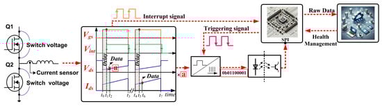
Figure 1.
Proposed condition monitoring approach for SiC-based DAB.
2.1. Proposed Sensor Technology
Figure 2a illustrates a DAB converter with blocks representing the units for capturing Vds,on and Ids,on. To measure the switch current, a current transformer (CT) is employed to assess the primary side current of the transformer (IL). It is essential to note that, depending on the conduction of the upper switches or the lower switches, IL is equal to the current passing through one pair of switches in the primary side. Consequently, IL can be considered as the switch current during the turn-on stage.
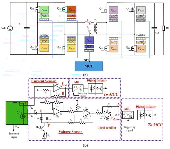
Figure 2.
Proposed CM system for monitoring critical electrical parameters: (a) DAB schematic with CM system, (b) Vds,on and Ids,on measurement unit, including capturing on-state voltage and current, digital isolator, and an ideal rectifier.
After capturing the on-state voltage and current signals of the switch, they are converted to a digital format. With circuit isolation, all data is transmitted to the MCU via the SPI protocol. Each color in the figure represents a different ground (GND) domain. Ultimately, after implementing circuit isolation, all signals share the same ground, shown in blue. The Section 2.2 provides a detailed explanation of how to capture the window and its time interval.
To gain a better understanding of signal capture, as well as digitalization and GND isolation, Figure 2b is provided. This figure illustrates the schematic of the sensorics used for CM of the SiC-based DAB. Similar to the Voltage Sensor section illustrated in the figure, a standard diode op-amp configuration is utilized to block the DC link voltage [23]. Additionally, an ideal rectifier is added downstream to rectify the voltage when the SiC MOSFET conducts from source to drain. It is called ideal because it does not alter the measured voltage. In addition, the minimum value of bias current created by the BJT, referred to as Ik, must be set at a level that ensures diodes D1 and D3 are suitably biased during the conduction of MOSFET Q12. This current affects the discharge of the junction capacitance associated with D1 and D3. Modifying Ik allows control over the discharge duration of these diodes, which in turn affects the fall time of Vds. This fall time reflects the transition of Q12 from the blocking state to conduction. As a result, the voltage at node F can be adjusted. In addition, for the current sensor, the IL is measured using the CT. To amplify this current, an op-amp is employed, resulting in an output denoted as ILa at node B. Finally, this output, Ila, is digitized and transmitted to the MCU as Ids,on.
Furthermore, selecting a suitable operational amplifier is essential. Important parameters to consider include common-mode and differential input voltage ranges, slew rate, bandwidth, output voltage swing, and, in particular, the common-mode rejection ratio (CMRR). Additionally, positioning the circuit as close as possible to the DUT is critical for minimizing parasitic capacitance and inductance. That is because as the switching frequency increases, the impedance introduced by these parasitic elements exceeds, posing significant errors in measurement Rds,on in an SiC MOSFET [3].
Moreover, recent studies have used analog isolators for isolation purposes. However, these isolators with limited bandwidths introduce rising/falling delays and propagation delays, which limit their effectiveness at higher switching frequencies and high rates of DC-link voltage changes (dv/dt) [3].
The proposed method in this paper addresses these limitations by employing digital isolation and an analog-to-digital converter (ADC). Since the ADC’s sampling rates, conversion, and transfer times can extend to several microseconds (µs) in this application, a triggering system has been implemented to optimize performance and reduce data size. In this research paper, the proposed circuit processes gate or drain–source signals, detects rising and falling edges, and triggers the MCU interrupt system. The MCU then commands the ADC to sample the current and voltage at specific times and transmits the data. Given the time required for conversion, acquisition, and data transmission, capturing multiple samples within a single switching period is not feasible. Figure 3 illustrates how the interrupt signal (Vint) event triggers the MCU, along with the gate-source signal (Vgs), drain–source voltage (Vds), and switch current (Ids). Furthermore, it should be noted that before sending Vint to the MCU to initiate the interrupt, an adequate delay is required. This delay compensates for oscillations during the switch turn-on process and accounts for the slew rate and fall time delay introduced by the op-amp. It ensures that the circuit reaches a steady state before sampling. The delay is implemented using an RC filter and a Schmitt trigger IC. It should be noted that an analog delay is essential, as implementing it digitally in the MCU could introduce inconsistencies in high-power applications, leading to unpredictable delay variations. In this figure, time t0 represents the moment the switch turns on. After the delay period, which is caused by the RC circuit, the interrupt signal is generated at t1, prompting the MCU to trigger the ADC, which then samples the voltage at point A in Figure 2b. Notably, a short additional delay occurs within the MCU, meaning the ADC effectively captures data at t2. Moreover, to establish a correlation between voltage and current, the current is sampled in the next switching cycle at t6, corresponding to point B in Figure 2b.
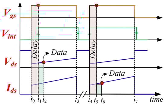
Figure 3.
Triggering and delay approach for data collection and synchronization between on-state voltage and current sampling. From top to bottom: gate-source voltage (Vgs), interrupt signal (Vint), drain–source voltage (Vds), drain–source current (Ids).
2.2. Data Acquisition Technique
Figure 4 presents the flowchart of the data acquisition technique used to capture the on-state voltage and current of the SiC MOSFET in the DAB converter. The process begins with the MCU waiting for an interrupt signal. Based on whether the voltage sensor or the current sensor is activated, the corresponding next step is executed.
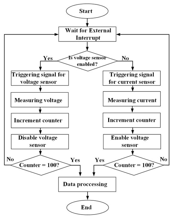
Figure 4.
Flowchart for data acquisition technique to capture the on-state voltage and current in SiC-based DAB.
To ensure accurate correlation between voltage and current, voltage is measured during one interrupt, while current is captured in the next interrupt. Once an interrupt occurs, a triggering signal is generated, prompting the ADC to initiate sampling and data acquisition.
The process then advances by incrementing a counter and disabling the active sensor, allowing the other sensor to operate during the subsequent interrupt. In this research, 100 voltage and current samples are collected. To reduce noise and eliminate outliers, the first and last 20% of the data are discarded, and the remaining values are averaged to produce the final result. The following section provides the data acquisition technique in detail. The primary drawback of this technique is evident in AC-DC or DC-AC converters, where line frequency components can significantly impact the current and voltage waveforms. In such instances, consecutive measurements of voltage and current might require a longer acquisition time. To capture data accurately, it is necessary to take a few measurements per line frequency cycle, leading to extra waiting time between successive measurements.
2.3. Cloud Connectivity
The methodology employed in the research regarding cloud connectivity and the estimation of the remaining useful lifetime for the SiC-based DAB converter, derived from measured Vds,on and Ids,on, is summarized in Figure 5. This section outlines the steps required for real-time RUL estimation of an SiC-based PEC. The developed software solution for RUL estimation is designed as an IoT edge–cloud system, where the edge node continuously transmits real-time data to the cloud for further processing. A Tinker Board 2.0 (Asus) Single Board Computer (SBC) is the edge device used for data collection and communication with cloud services. This device has WiFi and an onboard Universal Serial Receiver/Transmitter (UART) communication hardware. The sensed and filtered Vds,on and Ids,on data collected by the MCU are transmitted to the edge device via UART. The edge device then transmits the collected data in binary format, including metadata such as the test setup and data collection timestamp, to cloud storage via Hypertext Transfer Protocol Secure (HTTPS) and the cloud IP address through File Transfer Protocol (FTP), with cloud policies ensuring that only the edge device with a specific access key can send data.
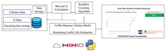
Figure 5.
Edge–cloud connectivity for predictive health monitoring of PECs and model-based estimation of the remaining useful lifetime utilizing measured Vds,on and Ids,on data.
To develop the cloud system, a brand-independent and open-source Minio Cloud Object Storage platform is utilized. This cloud solution supports remote data storage and is compatible with the Amazon Simple Storage Service (Amazon S3) format. The local cloud system runs a Python-based application for RUL estimation, utilizing Pandas, NumPy, and SciPy modules for efficient mathematical calculations and data storage. The Python application runs the following computations and algorithms: Tj calculation, Rain flow cycle counting algorithm on a batch of Tj data, Coffin Manson lifetime model calculation, and RUL estimator. The edge device continuously transfers Vds,on and Ids,on data to the cloud, where it is stored as objects with timestamps. Additionally, the cloud tracks the number of received (Vds,on, Ids,on) data points.
The cloud executes the RUL estimation algorithm, implemented in Python. The Python application interfaces with the Minio cloud in real-time to fetch incoming data points, process them for RUL calculations, and save the results in the Minio cloud storage. Since power switch degradation is assessed based on a batch of collected data, the cloud software waits until 1000 (Vds,on, Ids,on) data points are received before processing the batch for RUL estimation. For the lifetime model, the Vds,on, Ids,on data needs to be converted into the SiC MOSFET junction temperature (Tj). This temperature estimation is performed using a regression model that predicts Tj from the measured Vds,on and Ids,on values. The regression model is being developed based on the relationship between Vds,on, Ids,on, and Tj provided in the device datasheet. To further improve accuracy, additional real-world data will be collected through commissioning tests.
Once Tj is estimated, it is processed using the Rain flow Cycle Counting Algorithm (RCCA) to extract stress–strain data from the batch of Tj values. The RCCA output is then fed into a lifetime model to predict the number of cycles before failure (Nf) for each processed RCCA output. Finally, the total damage for a batch is calculated using Miner’s cumulative damage rule, as shown in Equation (1) [24].
where Dx represents the total calculated damage from the current batch number (x) of Tj data, ni is the number of cycles experienced at stress level i, and Nfi is the number of cycles before failure at stress level i.
The accumulated damage at any given time, while a batch is being processed, is the sum of the damage from all previous batches of Tj data up to that point. The total accumulated damage of the SiC MOSFET is calculated as follows:
The cloud stores the list of calculated damage for each batch, , with a time-stamp as .
A regression model is developed to predict when the total accumulated damage will reach its final value 1. This model can also be used to predict future values of , enabling accurate estimation of the RUL of the SiC MOSFET. Afterward, the overall DAB converter lifetime is assessed based on the system configuration of MOSFETs and diodes (i.e., series/parallel). A visualization tool has also been developed for data representation in the cloud environment, utilizing Python (version 3.13.5) and the Streamlit web app server (https://streamlit.io/, accessed on 1 March 2025). The visualization tool is an HTML page that showcases the real-time RUL calculation results. The list below showcases the overall algorithm used in the cloud for lifetime estimation.
- Initialize Minio cloud storage and data structures for sensor data (Vds,on, Ids,on, Rds, Tj) and accumulated damage; load existing damage data.
- Fetch Vds,on, Ids,on from Minio, calculate Rds (Vds,on/Ids,on), and estimate Tj using a regression model.
- Collect 1000 Tj values per batch.
- Apply Rain flow Cycle Counting Algorithm to extract stress cycles; compute damage using Miner’s rule.
- Predict RUL with a regression model based on accumulated damage.
- Store damage and RUL in Minio; visualize results on a Streamlit HTML dashboard.
The methodology described above effectively supports real-time RUL estimation using a single edge device with cloud integration. However, to enhance the edge–cloud framework for multi-device scalability and support for heterogeneous datasets, further development is necessary. In particular, fleet-level RUL estimation—where similar PECs transmit Tj data to the cloud—can benefit from federated learning approaches. Recent studies have proposed frameworks such as the Dynamic Barycenter Bridging Network (DBBN) and the Balance Recovery and Collaborative Adaptation (BRCA) method, which enable robust knowledge transfer across distributed edge nodes [25]. These approaches promote data decentralization while improving overall system scalability and feasibility for multi-site deployments, especially in scenarios where direct data sharing is constrained by privacy or bandwidth limitations.
3. Prototyping and Experimental Results
3.1. Experimental Results and Analysis
To assess the effectiveness of the proposed method, a CM circuit is built and tested, as illustrated in Figure 6. An STM32F407 Discovery Board (STMicroelectronics, Geneva, Switzerland) and a Tinker Board S R2.0 (ASUSTeK Computer Inc., Taipei, Taiwan) serve as edge devices for triggering and measuring data through the SPI protocol, facilitating the transmission of collected data to the cloud. The 7 kW DAB converter is evaluated at a switching frequency fsw = 35 kHz and an output voltage of 500 V, using double-sided cooled MOSFET switches (1200 V, 190 A, 7.2 mΩ). A Rogowski coil (CWTMini50HF/1, Power Electronic Measurements Ltd. (PEM UK), Nottingham, UK) is employed to measure and display the current IL on the oscilloscope.
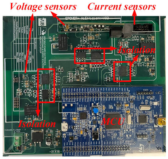
Figure 6.
Hardware prototype to capture the on-state voltage and current in SiC MOSFET.
A 1:150 current transformer is also utilized to measure IL and transmit the data to the MCU. After capturing the necessary signals via SPI with the STM32, the data is sent through a serial connection to the edge device and subsequently relayed to the cloud via the internet, which was locally linked to a PC. In the cloud, all data is processed, and the RUL, along with the junction temperature and captured signals, are displayed on a customized GUI.
The DAB converter test bench is shown in Figure 7. The phase current (IL in Figure 2) is measured using a current transformer placed in series with the primary side of the transformer in the DAB. When a switch turns on, the measured phase current corresponds directly to the current flowing through that switch.
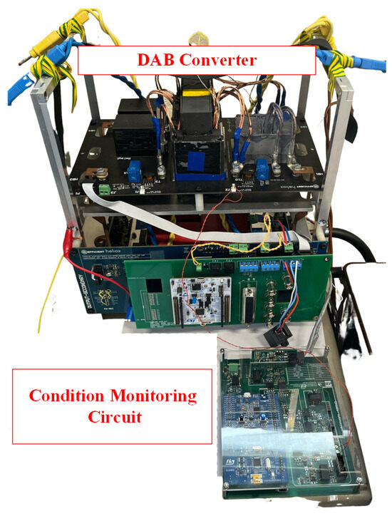
Figure 7.
7 kW DSC-SiC-based DAB converter test bench setup, including a CM circuit for measuring the on-state voltage (Vds,on) and current (Ids,on), and integrated with an MCU device.
Figure 8 illustrates the NOT gate-source voltage (Vgs), interrupt signal (Vint), triggering signal (Vtrig), and transformer current (IL) for DUT Q12. As shown in Figure 1, Vint and Vtrig correspond to the triggering signal and interrupt signals. Additionally, in Figure 2b, IL is measured at node B in the current sensor section. Since the implemented triggering system operates based on the falling edge of the signal, the Vgs of the upper switch, Q11, is utilized for triggering.
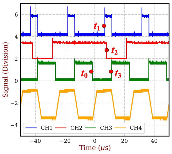
Figure 8.
Waveforms capturing key signals during operation. From top to bottom: CH1-interrupt signal Vint (1.6 V/div), CH2-triggering signal Vtrig (1.6 V/div), CH3-NOT gate-signal Vgs (1.6 V/div), CH4-transformer current IL (40 A/div). Test condition: Pout = 7 kW, fsw = 35 kHz, Vdc = 350 V.
Figure 8 depicts the Vgs of the upper switch, Q11, which operates in a complementary manner to that of Q12. This is why the signal is labeled as NOT Vgs. As a result, the rising edge of Q12’s gate-source voltage corresponds to the falling edge of Q11. Moreover, the time points t0 to t3 are labeled based on the timing sequence shown in Figure 3, where t0 marks the moment the DUT is turned on, t1 represents the time when the interrupt signal ends to the MCU, t2 indicates the moment the MCU begins triggering the ADC, and finally, at t3, the DUT turns off.
Additionally, Figure 9 shows the drain–source voltage (Vds) while the off-state voltage is blocked. This indicates the measurement at node A, as shown in Figure 2b.
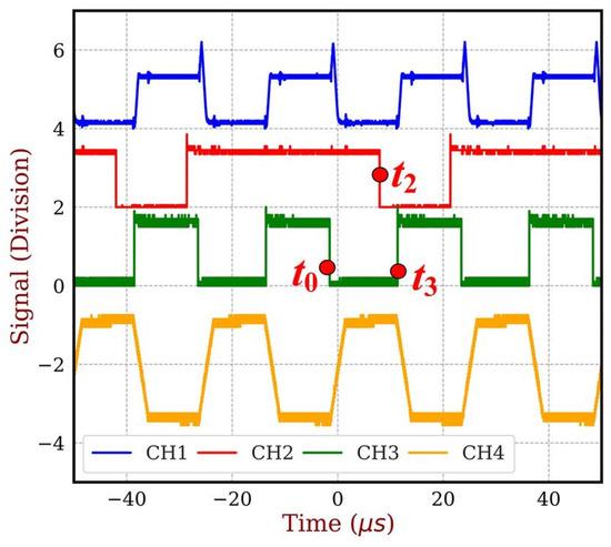
Figure 9.
Waveforms capturing key signals during operation. From top to bottom: CH1-switch drain–source voltage Vds (1.6 V/div), CH2-triggering signal Vint (1.6 V/div), CH3-NOT gate-signal Vgs (1.6 V/div), CH4-transformer current IL (40 A/div). Test condition: Pout = 7 kW, fsw = 35 kHz, Vdc = 350 V.
The output results from the MCU are presented in Figure 10, which details the voltage and current during the switch turn-on period. To achieve accurate validation, a constant load (i.e., 7 kW) is applied to the DAB while varying the coolant temperature between 40 °C and 80 °C. Due to the high thermal time constant of the DAB coolant system, the system requires a significant duration to reach the target temperature, resulting in a slow variation in the measured Vds,on. The nearly constant Ids,on confirms that the load condition remains fixed, allowing Vds,on variations to be attributed mainly to temperature effects. To assess the variations in junction temperature of the DUT, the Negative Temperature Coefficient (NTC) sensor, which is integrated into the DUT package, serves as a reference point for measurement. As shown in Figure 11, the measured temperature through NTC (TNTCT) follows changes in coolant temperature. Additionally, the on-state drain–source resistance (Rds,exp) is determined experimentally from the measured on-state voltage and current. The observed changes in Rds,exp are related to variations in TNTC, emphasizing the precision of the proposed condition monitoring circuit. However, a more comprehensive accuracy analysis is still required, and is addressed in the following section.
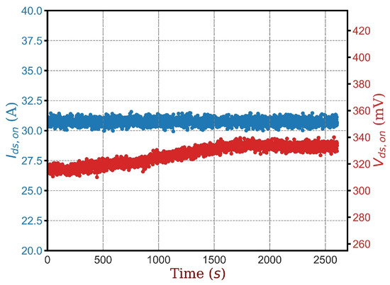
Figure 10.
Test results of CM of DAB converter, switch on-state current (Ids,on), and switch on-state voltage (Vds,on), while the coolant temperature is varied between 40 °C and 80 °C.
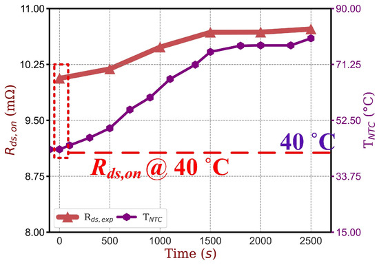
Figure 11.
Test results of CM of the DAB converter, switch on-state resistance (Rds,on), and switch junction temperature measured by NTC (TNTC), while the coolant temperature is varied between 40 °C and 80 °C.
3.2. Error Analysis
To establish a baseline for analyzing measurement errors, a calibration test (or commissioning test) is conducted in the laboratory using only the DUT. This test aims to map Rds,on to the junction temperature. The calibration tests for the DUT are performed using a source meter (Keysight B2902A, Keysight Technologies, Inc., Santa Rosa, CA, USA) at temperatures ranging from 40 °C to 80 °C [26]. The testing process begins by heating the DUT using an external heater, while an internal NTC sensor embedded within the DUT monitors its temperature. After reaching the target temperature, measurements are recorded by adjusting the gate voltage from 0 to 18 V using the Keysight 2902A while maintaining a drain–source voltage of 0.01 V. This setup enables the calculation of drain–source current and, subsequently, drain–source resistance. The resistance measured during this characterization process is referred to as Rds,chr. The relationship between Rds,chr, and junction temperature is illustrated in Figure 12. The regression analysis is performed in Python utilizing a simple linear least squares approach. It models the relationship between the junction temperature, Tj, and the measured on-state resistance, Rds,chr, using data points collected across the temperature range, as illustrated in Figure 12. The results showed a good fit, with an R-squared of approximately 0.98, demonstrating a strong linear correlation. The resulting equation is displayed in Equation (3).
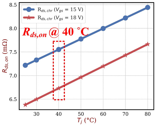
Figure 12.
Characterization results of a double-sided cooled MOSFET, illustrating the relationship between the switch on-state resistance (Rds,on) and the switch junction temperature, which varies from 40 °C to 80 °C.
In the following sections of the paper, two types of Rds,on are discussed as follows:
- Rds,chr: This value is calculated using Equation (3) and the NTC temperature (TNTC) measured during calibration or during operation at 7 kW.
- Rds,exp: This value is directly measured by the condition monitoring circuit while the system is running at 7 kW.
During the operation period, the NTC temperature is recorded, and Equation (3) is used to calculate the corresponding resistance value, referred to as Rds,chr. This computed value serves as the baseline for comparison with the experimentally measured resistance from the condition monitoring circuit, Rds,exp.
Figure 13 shows the evolution of three different Rds,on values over time during the test: the experimentally measured value Rds,exp, the value extracted from characterization Rds,chr, and the adjusted value Rds,adj. Although the difference between Rds,exp, and Rds,chr is approximately 2.3 mΩ, this deviation is not solely caused by incorrect measurement. It is also influenced by factors such as switching dynamics and parasitic elements in the measurement path.
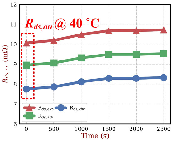
Figure 13.
Measured on-state resistance by condition monitoring circuit (Rds,ext), characterized on-state resistance (Rds,chr), and modified characterized on-state resistance (Rds,adj).
The adjusted value Rds,adj is introduced to reduce this offset and improve the consistency of the measured trend. It helps achieve a more stable and fair evaluation of device behavior over time, minimizing the impact of non-idealities that can distort raw resistance measurements.
An important consideration in implementing CM based on Rds,on in a measurement, is the influence of parasitic impedance. This impedance arises from two primary factors: stray inductance (Lstray) of the DUT and the DUT’s drain–source capacitance (Cds). The effect of these parasitic elements becomes more significant at higher switching frequencies. At these frequencies, the capacitive and inductive elements create a reactive voltage divider that distorts the measured drain–source voltage during conduction. Consequently, the observed Vds,on reflects not only the resistive drop across Rds,on but also a frequency-dependent error resulting from energy stored in and released from parasitic component elements. This behavior is represented by the following equation, which defines the equivalent impedance (Zeq) as a combination of parasitic impedance and Rds,chr [3]:
According to the DUT datasheet and routing, the stray inductance measures approximately 16 nH, and the Cds value is about 0.5 nF. The switching frequency is set to 35 kHz. Additionally, Rds,chr is derived from Figure 12 at Vgs = 15 V and Tj of 40 °C. Based on these values, the equivalent impedance is calculated as follows:
Using Equation (5) along with the measured characterization value at 40 °C (7.5 mΩ), we can conclude that the error from parasitic impedance is about 1.2 mΩ. Consequently, to account for this deviation, the characterized resistance value Rds,chr is adjusted by incorporating the parasitic elements’ impact. This adjusted resistance value is referred to as Rds,adj, and is presented in Figure 13. This correction guarantees that the resulting Rds,adj accurately represents the intrinsic channel resistance, free from switching-related artifacts.
To better understand the relationship between the experimentally measured Rds,exp, and the adjusted value Rds,adj, a regression analysis is performed. The resulting equation is as follows:
In Equation (6), the regression model’s coefficient of 1.15 is close to one, which indicates that the adjusted values effectively follow the degradation trend of Rds,on. This means that, despite accounting for parasitic effects, the adjusted values still reflect the aging signature of the device. This suggests that the proposed method can successfully track aging behavior during device operation. However, there is still an approximate error of 1.1 mΩ between the experimental data (Rds,exp) and the adjusted values from Equation (6) (Rds,adj). This offset can introduce inaccuracies in temperature estimation, especially in applications where precise thermal tracking is critical.
Nonetheless, since the slope of 1.15 is already close to unity, further testing and calibration can help reduce the offset and bring the adjusted and measured values into closer agreement. This approach is promising for practical degradation monitoring, even if some refinement is still needed.
To further investigate the cause of this remaining discrepancy, a noise analysis is required, which will be discussed in the following section.
3.3. Noise Analysis
Signal integrity poses a significant challenge in PECs, particularly in systems equipped with condition monitoring circuits. This issue is worsened by the high dv/dt switching transients of SiC MOSFETs, which can cause EMI- and noise-related malfunctions. Each voltage sensor in this setup is equipped with a digital isolator and a dedicated measurement ground. However, parasitic coupling capacitors (Cp) create common-mode (CM) noise pathways, as shown in Figure 14.
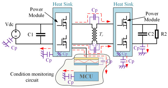
Figure 14.
Depiction of common-mode noise in the DAB converter and the circuitry for condition monitoring.
During switching transients, large amounts of common-mode current pass through these parasitic capacitors, making noise mitigation a significant concern. To address this, ferrite common-mode chokes and Y capacitors are incorporated into the noise paths.
To attenuate high-frequency common-mode noise generated by the fast dv/dt transitions of SiC MOSFETs, a common-mode choke is implemented using a MAGNETEC M-112 nanoperm core. The core is wound with two turns, resulting in a total inductance of approximately 52 µH at 100 kHz. This design ensures effective suppression of high-frequency noise without introducing significant voltage drop or interfering with regular circuit operation.
Similarly, Y capacitors are selected to provide a low-impedance path for high-frequency common-mode noise while maintaining safe leakage current levels, as required by EMC and insulation standards. Typically, values of 1–100 nF per capacitor are used, which is enough to bypass high-frequency noise in the MHz range while keeping the leakage current within acceptable limits for low-voltage systems and isolated signal paths [27]. In this paper, a total of 30 nF Y capacitors are used.
Common-mode current through using a Rogowski coil before and after adding a common-mode filter is illustrated in Figure 15. Experimental results in Figure 15b show that common-mode chokes effectively eliminate peaks in the common-mode current. Nevertheless, despite these improvements, the condition monitoring circuit still experiences residual common-mode noise. Additional mitigation approaches—such as employing ferrite beads or optical fiber for signal transmission—need further exploration. Based on these findings, the authors suggest that the remaining 1.1 mΩ error in the Rds,on measurement, is due to the influence of residual common-mode noise.
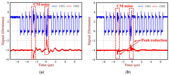
Figure 15.
Experimental waveforms illustrating the influence of the common-mode choke on the common-mode current (ICM) of the DAB converter and the SPI clock signal. CH1–SPI clock signal (1 V/div), CH2–ICM (2.4 A/div). (a) Without common-mode chokes, (b) with common-mode chokes.
4. Conclusions and Outlook
This research paper presents the development of an improved condition monitoring system for SiC-based PEC applications, featuring real-time cloud connectivity. The proposed CM circuit has been successfully integrated into a DAB converter, delivering 7 kW of output power at a switching frequency of 35 kHz, with reliable measurements demonstrated across a temperature range of 40 °C to 80 °C. We observed 1.2 mΩ deviation caused by parasitic impedance. To correct this, the characterized resistance value, Rds,chr, is adjusted to account for the impact of these parasitic elements.
However, the results indicate that this monitoring circuit still exhibits a minor error when measuring the actual Rds,on, with a maximum discrepancy of approximately 1.1 mΩ. This slight error is mainly due to common-mode noise and the very low value of Rds,on, making even small variations result in significant errors in estimating the junction temperature. The regression coefficient of 1.15, close to one, indicates that the circuit effectively monitors Rds,on degradation. With additional calibration and extended testing, this offset can be reduced, further improving the accuracy of both degradation and junction temperature measurements.
Furthermore, the integration of cloud processing enabled long-term data storage and analysis for evaluating accumulated damage, significantly enhancing the system’s capability to predict potential device degradation. By incorporating delay circuits and data processing techniques, the system effectively mitigated noise and ensured accurate data collection during switching transitions. Testing under actual conditions demonstrated the system’s ability to track degradation trends. Nonetheless, challenges persist in accurately estimating junction temperature, given the sensitivity of low resistance values and the impact of cable length and noise.
The overarching future ambition is to develop a robust measurement system with high accuracy for high-power converters seamlessly integrated with an intelligent data analytics layer. This system will function as a condition monitoring unit, providing advanced reliability and maintenance analysis capabilities based on the condition data of monitored assets in power electronic environments.
Author Contributions
Conceptualization, F.H., S.K.B., H.P. and S.C.; methodology, F.H. and S.C.; investigation, F.H., S.K.B., H.P. and S.C.; writing—original draft, F.H. and S.K.B.; writing—review and editing, F.H., S.K.B., S.C. and O.H.; supervision, S.C. and O.H.; funding acquisition, O.H. All authors have read and agreed to the published version of the manuscript.
Funding
This work was supported in part by the HiEFFICIENT Project, in part by the ECSEL Joint Undertaking (JU) under Grant 101007281 through the European Union’s Horizon 2020 Research and Innovation Program and Austria, Germany, Slovenia, The Netherlands, Belgium, Slovakia, France, Italy, and Türkiye.
Data Availability Statement
Dataset available on request from the authors.
Conflicts of Interest
The authors all were employed by the Flanders Make company. All authors declare that the research was conducted in the absence of any commercial or financial relationships that could be construed as a potential conflict of interest.
References
- Hosseinabadi, F.; Chakraborty, S.; Bhoi, S.K.; Prochart, G.; Hrvanovic, D.; Hegazy, O. A Comprehensive Overview of Reliability Assessment Strategies and Testing of Power Electronics Converters. IEEE Open J. Power Electron. 2024, 5, 473–512. [Google Scholar] [CrossRef]
- Power Electronics Market Size, Share & Industry Analysis, by Device Type (Power Discrete, Power Module, and Power IC), by Material (Silicon, GaN, SiC, and Others), by End-User (Consumer Electronics, Automotive, Industrial, Biomedical and Healthcare, Aerospace and Defense, and Others), and Regional Forecast, 2024–2032. Available online: https://www.fortunebusinessinsights.com/power-electronics-market-102595 (accessed on 1 March 2025).
- Roy, C.; Kim, N.; Evans, D.; Gafford, J.; Parkhideh, B. Challenges and Implementation of Online In-Situ RDSON Measurement in a Three-Phase Inverter. IEEE Trans. Power Electron. 2024, 39, 11677–11686. [Google Scholar] [CrossRef]
- Karakaya, F.; Member, S.; Donnal, J.S.; Morgan, A.J. In-Situ Detection of Bond Wire Lift-Off Events in Operational SiC MOSFETs. IEEE Trans. Power Electron. 2024, 39, 16659–16672. [Google Scholar] [CrossRef]
- Pu, S.; Yang, F.; Vankayalapati, B.; Akin, B. Aging Mechanisms and Accelerated Lifetime Tests for SiC MOSFETs: An Overview. IEEE J. Emerg. Sel. Top. Power Electron. 2021, 10, 1232–1254. [Google Scholar] [CrossRef]
- Bahl, S. Achieving GaN Products with Lifetime Reliability. Tex. Instrum. 2021, 1–19. [Google Scholar]
- Mitrovic, V.; Fan, B.; Cao, Y.; Bai, Y.; Burgos, R.; Boroyevich, D. Phase Current Reconstruction, DC Link Voltage and R DS- ON Measurement Using Sensors Integrated on Gate Drivers for SiC MOSFET. In Proceedings of the 2023 22nd International Symposium on Power Electronics (Ee), Novi Sad, Serbia, 25–28 October 2023; pp. 1–6. [Google Scholar]
- Roy, C.; Kim, N.; Gafford, J.; Parkhideh, B. On-State Voltage Measurement of High-Side Power Transistors in Three-Phase Four-Leg Inverter for In-Situ Prognostics. In Proceedings of the 2021 IEEE Energy Conversion Congress and Exposition (ECCE), Vancouver, BC, Canada, 10–14 October 2021; pp. 2770–2776. [Google Scholar]
- Guacci, M.; Bortis, D.; Kolar, J.W. On-State Voltage Measurement of Fast Switching Power Semiconductors. CPSS Trans. Power Electron. Appl. 2018, 3, 163–176. [Google Scholar] [CrossRef]
- Biglarbegian, M.; Mostafavi, S.; Hauer, S.; Nibir, S.J.; Kim, N.; Cox, R.; Parkhideh, B. On Condition Monitoring of High Frequency Power GaN Converters with Adaptive Prognostics. In Proceedings of the 2018 IEEE Applied Power Electronics Conference and Exposition (APEC), San Antonio, TX, USA, 4–8 March 2018; pp. 1272–1279. [Google Scholar] [CrossRef]
- Asoodar, M.; Nahalparvari, M.; Zhang, Y.; Danielsson, C.; Nee, H.-P.; Blaabjerg, F. Accurate Condition Monitoring of Semiconductor Devices in Cascaded H-Bridge Modular Multilevel Converters. IEEE Trans. Power Electron. 2023, 38, 3870–3884. [Google Scholar] [CrossRef]
- Pu, S.; Yang, F.; Vankayalapati, B.T.; Ugur, E.; Xu, C.; Akin, B. A Practical On-Board SiC MOSFET Condition Monitoring Technique for Aging Detection. IEEE Trans. Ind. Appl. 2020, 56, 2828–2839. [Google Scholar] [CrossRef]
- Asoodar, M.; Member, S.; Nahalparvari, M. A Novel ON-State Resistance Estimation Technique for Online Condition Monitoring of Semiconductor Devices Under Noisy Conditions. IEEE Open J. Instrum. Meas. 2024, 3, 2768–7236. [Google Scholar] [CrossRef]
- Farhadi, M.; Vankayalapati, B.T.; Sajadi, R.; Akin, B. AC Power Cycling Test Setup and Condition Monitoring Tools for SiC-Based Traction Inverters. IEEE Trans. Veh. Technol. 2023, 72, 12728–12743. [Google Scholar] [CrossRef]
- Ni, Z.; Lyu, X.; Yadav, O.P.; Singh, B.N.; Zheng, S.; Cao, D. Overview of Real-Time Lifetime Prediction and Extension for SiC Power Converters. IEEE Trans. Power Electron. 2020, 35, 7765–7794. [Google Scholar] [CrossRef]
- Ugur, E.; Yang, F.; Pu, S.; Zhao, S.; Akin, B. Degradation Assessment and Precursor Identification for SiC MOSFETs under High Temp Cycling. IEEE Trans. Ind. Appl. 2019, 55, 2858–2867. [Google Scholar] [CrossRef]
- Li, R.; Wu, X.; Yang, S.; Sheng, K. Dynamic On-State Resistance Test and Evaluation of GaN Power Devices Under Hard- and Soft-Switching Conditions by Double and Multiple Pulses. IEEE Trans. Power Electron. 2019, 34, 1044–1053. [Google Scholar] [CrossRef]
- Brekel, W.; Duetemeyer, T.; Puk, G.; Schilling, O. Time Resolved in Situ Tvj Measurements of 6.5 KV IGBTs during Inverter Operation. Proc. PCIM Eur. 2009, 806–813. [Google Scholar]
- Fan, J.; Ma, D.; Wang, J.; Chinthavali, M.; Moorthy, R.S.K. Real-Time Condition Monitoring of Power Modules in Grid-Tied Power Converter. In Proceedings of the 2022 IEEE Energy Conversion Congress and Exposition (ECCE), Detroit, MI, USA, 9–13 October 2022; pp. 1–6. [Google Scholar]
- Deckers, M.; Van Cappellen, L.; Moschner, J.; Daenen, M.; Driesen, J. Real-Time MOSFET Condition Monitoring for Variable Mission Profiles with a Dual Extended Kalman Filter. IEEE Trans. Power Electron. 2024, 40, 2219–2234. [Google Scholar] [CrossRef]
- Bhoi, S.K.; Chakraborty, S.; Verbrugge, B.; Helsen, S.; Robyns, S.; El Baghdadi, M.; Hegazy, O. Intelligent Data-Driven Condition Monitoring of Power Electronics Systems Using Smart Edge–Cloud Framework. Internet Things 2024, 26, 101158. [Google Scholar] [CrossRef]
- IEEE Std 1856-2017; IEEE Standard Framework for Prognostics and Health Management of Electronic Systems. IEEE: Piscataway, NJ, USA, 2017; pp. 1–31. [CrossRef]
- Hu, K.; Liu, Z.; Yang, Y.; Iannuzzo, F.; Blaabjerg, F. Ensuring a Reliable Operation of Two-Level IGBT-Based Power Converters: A Review of Monitoring and Fault-Tolerant Approaches. IEEE Access 2020, 8, 89988–90022. [Google Scholar] [CrossRef]
- Verbrugge, B.; Rasool, H.; Hasan, M.M.; Chakraborty, S.; Geury, T.; El Baghdadi, M.; Hegazy, O. Reliability Assessment of SiC-Based Depot Charging Infrastructure with Smart and Bidirectional (V2X) Charging Strategies for Electric Buses. Energies 2022, 16, 153. [Google Scholar] [CrossRef]
- Yang, B.; Lei, Y.; Li, X.; Li, N.; Si, X.; Chen, C. A Dynamic Barycenter Bridging Network for Federated Transfer Fault Diagnosis in Machine Groups. Mech. Syst. Signal Process 2025, 230, 112605. [Google Scholar] [CrossRef]
- Keysight Technologies Keysight B2902A Precision Source/Measure Unit, 2-Ch, 100 FA, 210 V, 3 A DC, 10.5 A Pulse 2024. Available online: https://www.keysight.com/us/en/options/B2902A/precision-source-measure-unit-2-ch-100fa-210v-3a-dc-10-5a-pulse.html (accessed on 1 March 2025).
- Ab, E.R.G.O. Capacitors for RFI Suppression of the AC Line: Basic Facts 2025. Available online: https://www.minuszerodegrees.net/line_supression/evoxrifa_rfi_fact.pdf (accessed on 1 March 2025).
Disclaimer/Publisher’s Note: The statements, opinions and data contained in all publications are solely those of the individual author(s) and contributor(s) and not of MDPI and/or the editor(s). MDPI and/or the editor(s) disclaim responsibility for any injury to people or property resulting from any ideas, methods, instructions or products referred to in the content. |
© 2025 by the authors. Licensee MDPI, Basel, Switzerland. This article is an open access article distributed under the terms and conditions of the Creative Commons Attribution (CC BY) license (https://creativecommons.org/licenses/by/4.0/).