Abstract
In this paper, the accuracy of basic and advanced spiral inductor models for gallium nitride (GaN) integrated inductors is evaluated. Specifically, the experimental measurements of geometrically scaled circular spiral inductors, fabricated in a radio frequency (RF) GaN-on silicon technology, are exploited to estimate the errors of two lumped geometrically scalable models, i.e., a simple π-model with seven components and an advanced model with thirteen components. The comparison is performed by using either the standard performance parameters, such as inductance (L), quality factor (Q-factor), and self-resonance frequency (SRF), or the two-port scattering parameters (S-parameters). The comparison reveals that despite a higher complexity, the developed advanced model achieves a significant reduction in SRF percentage errors in a wide range of geometrical parameters, while enabling an accurate estimation of two-port S-parameters. Indeed, the correct evaluation of both SRF and two-port S-parameters is crucial to exploit the model in an actual circuit design environment by properly setting the inductor geometrical parameters to optimize RF performance.
1. Introduction
Spiral inductors are fundamental components in radio frequency (RF) integrated circuits (ICs) since they are essential in crucial functionalities, such as impedance matching, tuned resonant load, LC oscillator tanks, etc. Although inductor devices are usually available in most RF technologies, inductor modeling, which is required for effective RF IC design, is often not accurate enough, thus leading to an extensive use of electromagnetic (EM) simulations. In recent years, GaN-based High-Electron-Mobility Transistors (HEMTs) gained attention in high-power applications thanks to better voltage/current capability in a wide temperature operative range. However, very few works about inductor measurements and modeling have been published with regard to GaN technologies so far [1,2,3,4,5,6]. Specifically, an equivalent circuit extracted for a single inductor geometry was proposed in [5] while lumped scalable models were proposed only in [2,6]. While in silicon-based technologies, many inductor models with different topologies and fitting equations are available [7,8,9,10], GaN-based inductor modeling is still poor despite the increasing success of such technology, which could be a bottleneck in the future development of GaN RF ICs. Indeed, the lack of accurate geometrically scalable models for integrated inductors extends project timelines, since time-consuming electromagnetic (EM) simulations must be used in the very first design phase. Recently, neural networks, machine learning, or deep learning techniques have demonstrated interesting results in the automatic design of mm-wave ICs and component modeling [11,12,13,14,15,16,17,18].
In this paper, two lumped scalable models are used to estimate the electrical parameters of geometrically scaled spiral inductors fabricated with RF GaN technology on silicon for sub 6 GHz power applications. Specifically, the first is a basic π-model, like the one in [6], previously developed from EM-based data in a similar GaN technology. The latter is based on the model developed in [10] for silicon-based spiral inductors, which is here modified for the adopted GaN-on-silicon process. The accuracy of both models is evaluated and compared in terms of either standard performance parameters, such as inductance (L), quality factor (Q-factor), and self-resonance frequency (SRF) or the two-port scattering parameters (S-parameters). The comparison has been carried out by using on-wafer measurements of a circular spiral in a wide range of inductances and geometric parameters to evaluate model prediction capabilities as a RF IC design tool.
2. RF GaN Technology
This study has been carried out in an RF GaN process fabricated on a thin silicon (Si) substrate. This technology has been developed by STMicroelectronics, mainly for sub 6-GHz band power applications [18,19]. It includes 50-V HEMTs with a gate length of 0.5-µm, optimized for normally on depletion operation, thus exploiting the total two-dimensional electron gas (2DEG) density at the AlGaN/GaN heterointerface. The technology also provides resistors and high-Q-factor metal–insulator–metal (MIM) capacitors for the integration of biasing and matching networks, respectively, while allowing for the fabrication of polygonal/circular spiral inductors and interleaved/stacked transformers that are essential for advanced RF ICs [20,21,22,23,24,25,26]. The BEOL of the process consists of two top thick AlCu metals (namely MTL3 and MTL2), used for the inductor coil and the underpass, respectively, and a thinner AlCu layer for transistor connections. Specifically, the thickness of MTL3 and MTL2 is equal, which allows inductor series resistance to be reduced while avoiding possible current limitations due to the underpass connection. The adopted GaN technology has been developed for watt-level sub 6-GHz power amplifiers (PAs) for base station applications. The aim is to replace the traditional micromodule approach based on discrete components with a fully integrated system, thus achieving a significant reduction in cost and size.
Figure 1 shows the microphotograph of a circular inductor in the adopted RF GaN technology and the SEM micrograph of the upper metal layers, as they are connected in the underpass region of a spiral inductor. Specifically, as shown in Figure 1a, the coil exploits the top MTL3, while the underpass is implemented in MTL2. The circular geometry has been exploited to achieve better Q-factor performance than squared or polygonal shapes. The ground substrate electrical connection is provided by the trough–silicon–vias (TSVs) that also guarantee proper thermal dissipation, especially in high-power applications. It is worth noting that Figure 1 depicts the spiral inductor in a two-port test structure with ground–signal–ground (GSG) input/output pads (i.e., DUT) used for on-wafer measurement. On-wafer measurements have been performed by means of a two-port VNA by Keysight [27] connected to a 200-nm Cascade summit prober [28]. LRM calibration has been adopted [29,30]. A 5-step de-embedding procedure was adopted to remove the RLC parasitic and refer the measurement plane to the inductor terminals, highlighted in red in Figure 1a [31]. To this end, the de-embedding structures shown in Figure 2 were integrated and measured for each inductor geometry.
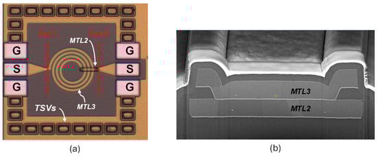
Figure 1.
Microphotograph of a spiral inductor in the RF GaN-on-Si technology (a); SEM micrograph of the inductor in the underpass region (b) [6].
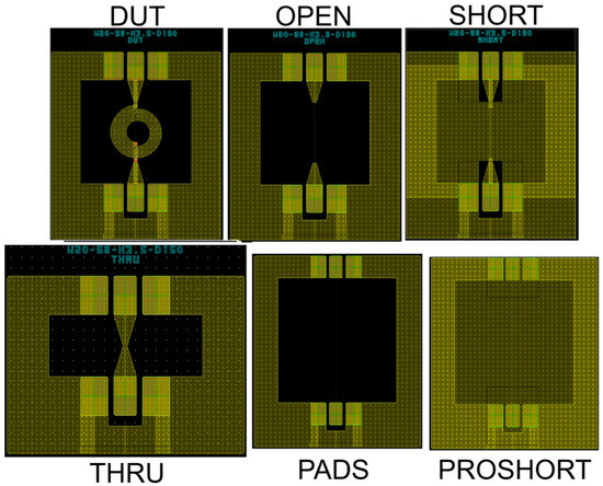
Figure 2.
DUT and de-embedding structures used for inductor on-wafer measurement.
3. Inductor Lumped Model Descriptions
Inductor modeling is mainly aimed at predicting the electrical performance of integrated inductors in a large range of inductance values, which is essential to RF IC design. Indeed, an accurate lumped scalable model allows setting of the geometrical parameters of a spiral inductor, which are shown in Figure 3, to comply with RF circuit specifications (i.e., L, Q-factor, SRF, maximum current, consumed area). The availability of accurate scalable modeling reduces the use of time-consuming EM simulations in the very last design phase, according to the scheme sketched in Figure 4.
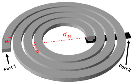
Figure 3.
Geometrical parameters of a spiral RF inductor.
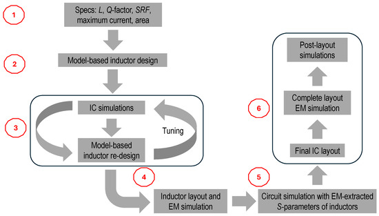
Figure 4.
Simplified design flow of integrated inductors for RF ICs.
In this work, two different lumped models are proposed and compared in terms of accuracy. The models have been mainly developed to cover the typical needs of sub 6-GHz PAs. Their schematics are depicted in Figure 5. The first model shown in Figure 5a has been developed starting from the simple model in [6], making some improvements to increase its accuracy. The latter, shown in Figure 5b, is inspired by a topology proposed for silicon-integrated inductor modeling in [10]. In the following subsections, geometrically scaled equations for lumped components are detailed for both proposed models.
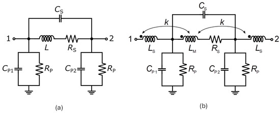
Figure 5.
GaN-on-Si inductor models under comparison (Terminal 2 is the underpass of the inductor): (a) lumped π-model; (b) advanced lumped model.
3.1. Lumped π-Model
With reference to Figure 5a, the ideal inductor, L, models both spiral and underpass inductances, as well as the substrate magnetic coupling. Two different capacitors, CP1 and CP2, account for the asymmetric substrate capacitive effects, while CS models the fringing capacitances between the spiral turns, and the overlap capacitance between the spiral and the underpass. Both ohmic and substrate losses are estimated by means of frequency-variable resistances, RS and RP, respectively.
Specifically, L consists of three inductances,
where LCOIL and LUND are the spiral and underpass inductances, respectively, while LSUB accounts for the induced magnetic field in the substrate [32,33,34]. The first two terms of (1) are calculated by means of closed form expressions [35,36]. On the other hand, LSUB adopts a similar monomial formula to [6], which better estimates the inductance reduction due to an induced magnetic field within the substrate:
where dAVG is the average inductor diameter, n is the number of turns, and w the metal width.
The capacitor, CS, is calculated by means of the same scalable equation used in [6]:
where NOVER is the number of overlaps between the spiral and the underpass (i.e., NOVER = n + 1.5), and εM and tM are the electric permittivity and the thickness of the intermetal (i.e., MTL3-MTL2) dielectric layer, respectively. However, to improve the geometrical scalability of (3), a different polynomial expression function p(n) is proposed in (4).
Substrate capacitances, CP1,2, are calculated by means of the same equations reported in [6] that for the sake of completeness are reported hereinafter:
where CSUB is the substrate capacitance per unit area, ACOIL is the coil area, α1 is a fitting parameter equal to 0.92, and β1 is an experimental coefficient estimated to be 3.53 × 10⁴. The coil area, ACOIL1,2, is given by the product of the width, w, and the spiral length, lCOIL1,2 that are calculated according to the following expressions, where dIN is the inner diameter:
An asymmetric spiral inductor has two slightly different values of self-resonance frequencies, SRF1 and SRF2, when Terminal 1 or Terminal 2 is grounded, respectively. To reproduce such asymmetry in the model, the capacitances CP1 and CP2 are calculated by expressions (6) and (7), respectively.
The series resistance, RS, is modeled as in [6]. Its expression is reported below for the sake of clarity:
where RDC is the overall dc resistance of the inductor, while fRM and fR0 are the frequencies for which RS assumes its maximum and zero, respectively. The values of fRM and fR0 are calculated by means of the different empirical formulas
Finally, substrate losses are modeled by means of RP according to the following novel expression:
where ρSi and tSi are the resistivity and the thickness of the silicon substrate, dOUT is the inductor outer diameter, and kp is equal to 10−20 Hz−1. It is worth noting that the adopted RP expression better predicts the resistive loss increase with frequency in comparison with the equivalent one reported in [6].
3.2. Advanced Lumped Model
The lumped model shown in Figure 5b is fully geometrically scalable as the first one, but it exploits an advanced topology with thirteen components. Thanks to a more distributed and coupled topology, it better predicts the two-port behavior of spiral inductors, that can hardly be modeled by using a simple π-like network [10].
To this aim, the inductance, L, which is still calculated by means of Equations (1) and (2), is split into three magnetically coupled components (i.e., LM and two equal inductances, LS) according to the spitting factor, ks. The expressions for LM and LS are reported below:
The magnetic coupling factor, k, has been set as equal to 0.5, assuming that, regardless of the inductor geometry, just half of the whole magnetic flux generated by LM is linked to LS. The splitting factor, kS, has been set to 2.5 × 10⁻² to fit the measured S-parameters.
The model exploits expressions (3) and (11) for CS and RP, respectively. On the other hand, CP1,2 is calculated by means of the improved Equations (14)–(16):
where CSUB is the substrate capacitance per unit area and dOUT is the external diameter of the spiral. The term (β2/w) accounts for the asymmetry of the capacitances CP1 and CP2 due to asymmetrical inductor layout. Moreover, it models the increase in capacitance due to fringing effects, which are relevant for small-width inductors. In this respect, similar considerations about the electric fringing phenomena affecting the substrate capacitances are reported in [6]. The parameter β2 has been set as equal to 2 µm.
Finally, thanks to inductance splitting and magnetic coupling, the topology allows adopting a physical expression to model the monotone increase in the series resistance, RS, due to current crowding phenomena [31,37,38,39,40], which is not possible in a simple π-like model such as the one shown in Figure 5a. Specifically, RS is modeled with Equations (17) and (18):
where RDC is the overall dc resistance of the inductor. The parameter α2 has been set as equal to 0.47 to model the normalized series resistance, RS/RDC, as shown in Figure 6. It is worth noting that RS is on average around three times its DC value for f = SFR1.
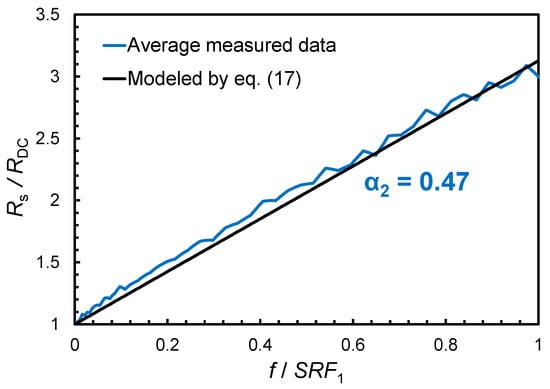
Figure 6.
Comparison between measured and modeled normalized series resistance.
Table 1 summarizes the dependencies of performance parameters on circuit components, fitting parameters and scalable equations for the advanced model in Figure 5b. A sensitivity analysis for the main performance parameters is instead reported in Table 2.

Table 1.
Performance parameter dependencies for the advanced model in Figure 5b.
Table 2.
Sensitivity analysis on performance parameters for 50% variations in the fitting parameters for the advanced model in Figure 5b (n = 1.5, w = 60 µm, dIN = 290 µm).
4. Model Validation and Comparison
The proposed lumped models have been validated by comparison with the experimental data of geometrically scaled circular inductors in a very wide range of geometrical parameters. Specifically, the turn number, n, spans from 1.5 to 6.5, the metal width, w, from 10 µm to 100 µm, and the inner diameters, dIN, from 60 µm to 300 µm, while the metal spacing, s, is fixed to the minimum technological value, i.e., 10 μm. In this work, special attention was given to covering a wide range of metal width, w (i.e., 10 µm to 100 µm), which is essential to achieve accuracy not only for low-current inductors, but also for high-current inductors in power applications. As far as the frequency range is concerned, both models have been developed to cover typical needs of sub 6-GHz power amplifiers and therefore they have not been validated for high-frequency inductors, i.e., inductors with SRF higher than 15 GHz, which exhibit a Q-factor peak well above 6 GHz.
The comparison is first carried out in terms of the common inductor performance parameters, such as L, Q-factor, and SRF. Indeed, such parameters, along with the maximum delivered current and consumed area, are largely adopted by RF IC designers to optimize the geometry of the inductor, as already shown in Figure 4.
Figure 7, Figure 8, Figure 9 and Figure 10 compare measured inductance and Q-factor curves versus frequency with the estimated behaviors of the two lumped models for four geometrically scaled inductors, whose layouts are shown for the sake of clarity. Figure 11 compares model-calculated values of low-frequency L, SRF, and Q-factor at 2 GHz with measured values. Both models approximate the low-frequency L with maximum errors below 8%. On the other hand, both SRF and Q-factor estimations are very challenging due to the very wide geometrical parameter range. Specifically, as far as the SRF is concerned, the π-based model in Figure 5a shows a lack of accuracy at the increasing of the metal width, w, with percentage errors as high as 13%. On the other hand, both models predict the Q-factor with good precision in the rising low-frequency region, where the skin effect is dominant, while showing growing errors at higher frequencies when current crowding is significant and resonance bend starts. The Q-factor peak frequency range is well predicted, but maximum Q-factor is affected by higher errors for both models. Finally, the advanced model in Figure 5b achieves better accuracy in the SRF prediction with maximum errors of about 3%.
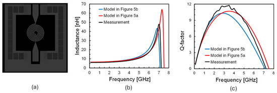
Figure 7.
Comparison between proposed models and measurements: (a) circular inductor layout (n = 6.5, w = 10 µm, dIN = 60 µm), (b) inductance versus frequency, (c) Q-factor versus frequency.
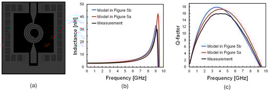
Figure 8.
Comparison between proposed models and measurements: (a) circular inductor layout (n = 3.5, w = 20 µm, dIN = 150 µm), (b) inductance versus frequency, (c) Q-factor versus frequency.
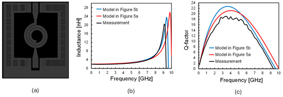
Figure 9.
Comparison between proposed models and measurements: (a) circular inductor layout (n = 2.5, w = 40 µm, dIN = 200 µm), (b) inductance versus frequency, (c) Q-factor versus frequency.
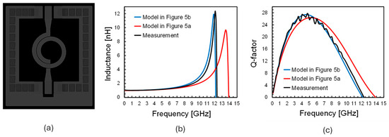
Figure 10.
Comparison between proposed models and measurements: (a) circular inductor layout (n = 1.5, w = 60 µm, dIN = 290 µm), (b) inductance versus frequency, (c) Q-factor versus frequency.
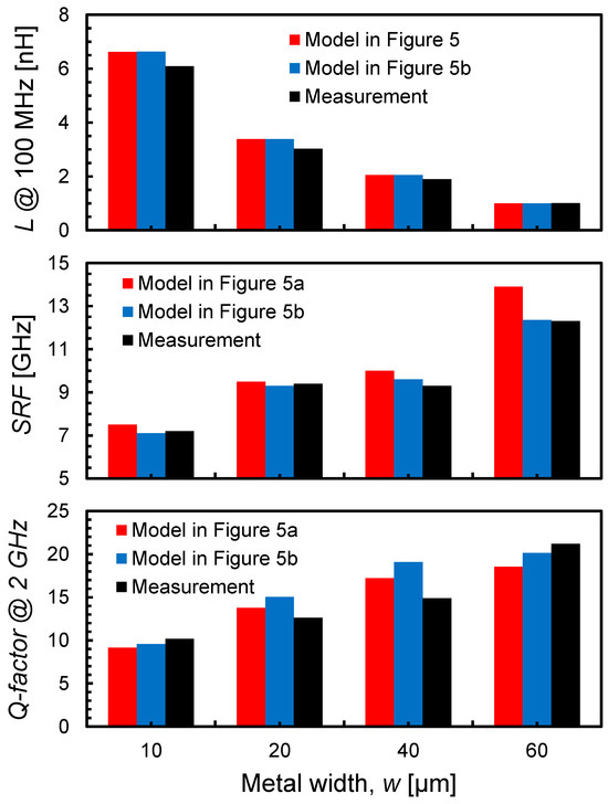
Figure 11.
Model comparison at different metal widths, w.
Discrepancies between models and measurements can be attributed to the substrate effects. Indeed, series losses due to current crowding are well predicted, as demonstrated by Figure 6, and therefore the residual error on the Q-factor is mainly ascribed to the substrate losses. It is worth noting that adopted silicon substrate exhibits frequency-dependent conductivity [6], which cannot be accurately modeled by a simple equation like (11) used in both presented models. The frequency dispersity could also explain the inductance discrepancies since the inducted magnetic field, expressed by LSUB in Equation (1), depends on the substrate conductivity.
The comparison between models has also been carried out in terms of two-port S-parameters in Figure 12, Figure 13, Figure 14 and Figure 15. Indeed, accurate S-parameter estimation is required to exploit lumped modeling in RF IC design, when inductor EM-extracted data are not available yet. Figure 11, Figure 12, Figure 13 and Figure 14 compare measured and modeled S-parameters (i.e., S11, S22, and S21) for the previously reported geometries. The comparison highlights that the S-parameter estimation of the π-model has significant discrepancies with respect to measurements, especially for higher w values. Moreover, the π-model shows its limits in predicting the transmission coefficient, S21, which is of high importance to evaluate inductor signal loss. On the other hand, Figure 10, Figure 11, Figure 12, Figure 13 and Figure 14 demonstrate that the advanced model in Figure 5b is well-suited to S-parameter prediction thanks to its topology.
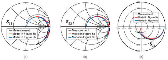
Figure 12.
Comparison between model-estimated and measured S-parameters: (a) S11, (b) S22, and (c) S21 (n = 6.5, w = 10 µm, dIN = 60 µm).
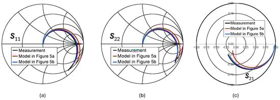
Figure 13.
Comparison between model-estimated and measured S-parameters: (a) S11, (b) S22, and (c) S21 (n = 3.5, w = 20 µm, dIN = 150 µm).
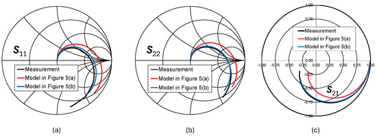
Figure 14.
Comparison between model-estimated and measured S-parameters: (a) S11, (b) S22, and (c) S21 (n = 2.5, w = 40 µm, dIN = 200 µm).
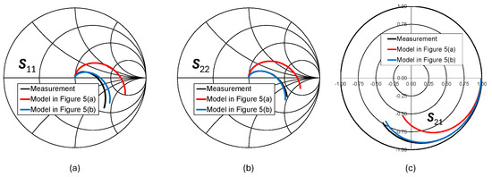
Figure 15.
Comparison between model-estimated and measured S-parameters: (a) S11, (b) S22, and (c) S21 (n = 1.5, w = 60 µm, dIN = 290 µm).
Specifically, the transmission coefficient, S21, is predicted with lower percentage errors compared to the simple π-model ones, as shown in Figure 16 for four scaled inductors.
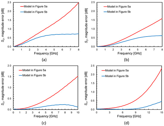
Figure 16.
S21 magnitude errors: (a) n = 6.5, w = 10 µm, dIN = 60 µm, (b) n = 3.5, w = 20 µm, dIN = 150 µm, and (c) n = 2.5, w = 40 µm, dIN = 200 µm, (d) n = 1.5, w = 60 µm, dIN = 290 µm.
The above results confirm the soundness of both lumped scalable models for GaN inductors that can be profitably used within the design flow in Figure 4 (steps 1–2), while the advanced model is more suited for the tuning phase (step 3) that requires accurate S-parameter estimation. To the author’s knowledge, this is the first time a fully scalable model has been experimentally validated for S-parameter prediction of GaN-on-Si inductors.
5. Conclusions
This study proposes and compares a π-based model and an advanced model for circular inductors in 0.5 µm RF GaN-on-Si technology for sub 6-GHz power applications. Both models are lumped and fully geometrically scalable. They demonstrate similar accuracy in predicting both L and Q-factor in a wide range of geometrical parameters, also including high-width values adopted for power applications. Moreover, thanks to its novel topology, the advanced model achieves improved accuracy in SRF, as well as in S- parameter estimation, which makes it highly suited to typical RF IC design flow. To the authors’ knowledge, this is the very first experimentally validated model for spiral inductors in RF GaN technology able to predict two-port S-parameters in a wide range of geometrical parameters. The high potentiality of the model suggests that in future work it could be extended either to a wider range of geometric parameters and therefore higher operative frequencies or for different shapes or structures (i.e., polygonal, multi-layer, symmetric, etc.). Finally, the model could also be improved by taking advantage of AI-based techniques that have already proven useful in this field.
Author Contributions
Conceptualization, S.S., G.S. and E.R.; validation, S.S. and G.S.; formal analysis, S.S.; methodology, S.S., G.S. and E.R.; project administration, E.R. and M.G.; supervision, E.R., G.S. and M.G.; writing—original draft, E.R.; writing—review and editing, S.S., G.S., M.G. and E.R. All authors have read and agreed to the published version of the manuscript.
Funding
This study was partially supported by STMicroelectronics under the Research Contract with the DIEEI titled “Progettazione e ottimizzazione di componenti passivi reattivi integrati per applicazioni 5G in tecnologia GaN on Si e relativa attività propedeutica per rilascio di un futuro design kit”.
Data Availability Statement
The data presented in this study is available on request from the corresponding author.
Conflicts of Interest
Simone Spataro, Giuseppina Sapone, and Marcello Giuffrida are employed by the company STMicroelectronics. The remaining author declares that the research was conducted in the absence of any commercial or financial relationships that could be construed as a potential conflict of interest.
References
- Eblabla, A.; Li, X.; Wallis, D.J.; Guiney, I.; Elgaid, K. High-performance MMIC inductors for GaN-on-low-resistivity silicon for microwave applications. IEEE Microw. Wirel. Compon. Lett. 2018, 28, 99–101. [Google Scholar] [CrossRef]
- Montesdeoca, M.S.M.; Angulo, S.M.; Duarte, D.M.; Del Pino, J.; García, J.A.G.Y.; Khemchandani, S.L. An analytical scalable lumped-element model for GaN on Si inductors. IEEE Access 2020, 8, 52863–52871. [Google Scholar] [CrossRef]
- Chander, S.; Bansal, K.; Gupta, S.; Gupta, M. Design and analysis of high performance air-bridge spiral circular inductors for GaN MMICs up to Ku band. In Proceedings of the 2017 Devices for Integrated Circuit (DevIC), Kalyani, India, 23–24 March 2017; pp. 734–736. [Google Scholar]
- Chander, S.; Bansal, K.; Gupta, S.; Gupta, M. Design and analysis of spiral circular inductors for GaN based low noise amplifier (MMICs). In Proceedings of the 2015 International Conference on Microwave, Optical and Communication Engineering (ICMOCE), Bhubaneswar, India, 18–20 December 2015; pp. 292–294. [Google Scholar]
- Wang, H.-S.; He, W.-L.; Wang, R.-D.; Zhang, M.-H. A double-π equivalent circuit model for GaN on-chip inductors. In Proceedings of the IEEE International Conference on Solid-State and Integrated Circuit Technology, Hangzhou, China, 25–28 October 2016; pp. 811–815. [Google Scholar]
- Spataro, S.; Sapone, G.; Giuffrida, M.; Ragonese, E. A geometrically scalable lumped model for spiral inductors in radio frequency GaN Technology on Silicon. Electronics 2024, 13, 2665. [Google Scholar] [CrossRef]
- Huo, X.; Chan, P.C.H.; Chen, K.J.; Luong, H.C. A physical model for on-chip spiral inductors with accurate substrate modeling. IEEE Trans. Electron Devices 2006, 53, 2942–2949. [Google Scholar] [CrossRef]
- Sia, C.B.; Ong, B.H.; Chan, K.W.; Yeo, K.S.; Ma, J.G.; Do, M.A. Physical layout design optimization of integrated spiral inductors for silicon-based RFIC applications. IEEE Trans. Electron Devices 2005, 52, 2559–2567. [Google Scholar] [CrossRef]
- El-Gharniti, O.; Kerherve, E.; Begueret, J.-B. Modeling and characterization of on-chip transformers for silicon RFIC. IEEE Trans. Microw. Theory Tech. 2007, 55, 607–615. [Google Scholar] [CrossRef]
- Scuderi, A.; Biondi, T.; Ragonese, E.; Palmisano, G. A lumped scalable model for silicon integrated spiral inductors. IEEE Trans. Circuits Syst. I Regul. Pap. 2004, 51, 1203–1209. [Google Scholar] [CrossRef]
- Krishna, S.R.; Narayana, J.L.; Reddy, L.P. A neural network inverse modeling approach for the design of spiral inductor. Int. J. Comput. Sci. Eng. Technol. (IJCSET) 2012, 2, 54–60. [Google Scholar]
- Dervenis, N.; Alexandridis, G.; Stafylopatis, A. Neural network specialists for inverse spiral inductor design. In Proceedings of the 2018 IEEE 30th International Conference on Tools with Artificial Intelligence (ICTAI), Volos, Greece, 5–7 November 2018; pp. 60–64. [Google Scholar]
- Abi, S.; Bouyghf, H.; Raihani, A.; Benhala, B. Swarm intelligence optimization techniques for an optimal RF integrated spiral inductor design. In Proceedings of the International Conference on Electronics, Control, Optimization and Computer Science (ICECOCS), Kenitra, Morocco, 29–30 November 2018; pp. 1–7. [Google Scholar]
- Guillod, T.; Papamanolis, P.; Kolar, J.W. Artificial neural network (ANN) based fast and accurate inductor modeling and design. IEEE Open J. Power Electron. 2020, 1, 284–299. [Google Scholar] [CrossRef]
- Lee, D.; Shin, G.; Lee, S.; Kim, K.; Oh, T.-H.; Song, H.-J. Neural-network-based automated synthesis of transformer matching circuits for RF amplifier design. IEEE Trans. Microw. Theory Tech. 2022, 70, 4726–4739. [Google Scholar] [CrossRef]
- Yin, S.; Wang, R.; Zhang, J.; Liu, X.; Wang, Y. Automatic design for W-band front-end system via bottom-up sizing and layout generation. IEEE Trans. Comput.-Aided Des. Integr. Circuits Syst. 2024, 43, 705–715. [Google Scholar] [CrossRef]
- Karahan, E.A.; Liu, Z.; Gupta, A.; Xu, X.; Hsu, S.L.; Zheng, J.; Sun, G.; Zhang, Z.; Xu, H.; Vaddiraju, S.; et al. Deep-learning enabled generalized inverse design of multi-port radio-frequency and sub-terahertz passives and integrated circuits. Nat. Commun. 2024, 15, 10734. [Google Scholar] [CrossRef] [PubMed]
- Vandendaele, W.; Leurquin, C.; Lavieville, R.; Jaud, M.A.; Viey, A.G.; Gwoziecki, R.; Mohamad, B.; Nowak, E.; Constant, A.; Iucolano, F. Reliability of GaN MOSc-HEMTs: From TDDB to threshold voltage instabilities (Invited). In Proceedings of the IEEE International Reliability Physics Symposium (IRPS), Monterey, CA, USA, 26–30 March 2023; pp. 1–8. [Google Scholar]
- Scandurra, A.; Testa, M.; Franzò, G.; Greco, G.; Roccaforte, F.; Castagna, M.E.; Calabretta, C.; Severino, A.; Iucolano, F.; Bruno, E.; et al. Isolation of bidimensional electron gas in AlGaN/GaN heterojunction using Ar ion implantation. Mater. Sci. Semicond. Process. 2023, 168, 107871. [Google Scholar] [CrossRef]
- Santhakumar, R.; Pei, Y.; Mishra, U.K.; York, R.A. Monolithic millimeter-wave distributed amplifiers using AlGaN/GaN HEMTs. In Proceedings of the IEEE MTT-S Int. Microwave Symposium Digest, Atlanta, GA, USA, 15–20 June 2008; pp. 1063–1066. [Google Scholar]
- Korndorfer, F.; Muhlhaus, V. Lumped modeling of integrated MIM capacitors for RF applications. In Proceedings of the Microwave Measurement Conference (ARFTG), Austin, TX, USA, 8–9 December 2016; pp. 1–4. [Google Scholar]
- Bevilacqua, A. Fundamentals of integrated transformers: From principles to applications. IEEE Solid-State Circuits Mag. 2020, 12, 86–100. [Google Scholar] [CrossRef]
- Long, J.R. Monolithic transformers for silicon RF IC design. IEEE J. Solid-State Circuits 2000, 35, 1368–1382. [Google Scholar] [CrossRef]
- Tripoli, D.; Maiellaro, G.; Pavone, S.C.; Ragonese, E. A low-phase-noise and area-efficient quad-core VCO based on stacked two-port inductors. IEEE Access 2024, 12, 87065–87076. [Google Scholar] [CrossRef]
- Tripoli, D.; Maiellaro, G.; Pavone, S.C.; Ragonese, E. Interstacked Transformer Quad-Core VCOs. Electronics 2024, 13, 927. [Google Scholar] [CrossRef]
- Papotto, G.; Nocera, C.; Finocchiaro, A.; Parisi, A.; Cavarra, A.; Castorina, A.; Ragonese, E.; Palmisano, G. A 27-mW W-band radar receiver with effective TX leakage suppression in 28-nm FD-SOI CMOS. IEEE Trans. Microw. Theory Tech. 2021, 69, 4132–4141. [Google Scholar] [CrossRef]
- Keysight. N5224B PNA Microwave Network Analyzer. 2025. Available online: https://www.keysight.com/us/en/product/N5224B/pna-microwave-network-analyzer-900-hz-10-mhz-43-5-ghz.html (accessed on 23 July 2025).
- Form Factor. Cascade Summit 200 mm Manual Probe System. 2025. Available online: https://www.formfactor.com/product/probe-systems/200-mm-systems/summit/ (accessed on 23 July 2025).
- Davidson, A.; Jones, K.; Strid, E. LRM and LRRM calibrations with automatic determination of load inductance. In Proceedings of the 36th ARFTG Conference Digest, Monterey, CA, USA, 29–30 November 1990; pp. 57–63. [Google Scholar]
- Shang, X.; Ding, J.; Ridler, N.; Buck, C.; Geen, M. Calibration Techniques for Millimetre-wave On-wafer S-parameter Measurements. In Proceedings of the ARMMS RF & Microwave Society Conference, Wyboston, UK, 18–19 November 2019; Available online: https://www.armms.org/media/uploads/xiaobang-shang---armms-nov-2019.pdf (accessed on 23 July 2025).
- Biondi, T.; Scuderi, A.; Ragonese, E.; Palmisano, G. Characterization and modeling of silicon integrated spiral inductors for high-frequency applications. Analog. Integr. Circuits Signal Process. 2007, 51, 89–100. [Google Scholar] [CrossRef]
- Kuhn, W.B.; Ibrahim, N.M. Analysis of current crowding effects in multiturn spiral inductors. IEEE Trans. Microw. Theory Tech. 2001, 49, 31–38. [Google Scholar] [CrossRef]
- Kuhn, W.B. Loss mechanisms and quality factor improvement for inductors in high-resistivity SOI processes. In Proceedings of the IEEE 12th Topical Meeting on Silicon Monolithic Integrated Circuits in RF Systems, Santa Clara, CA, USA, 16–18 January 2012; pp. 29–32. [Google Scholar]
- Kuhn, W.B.; He, S.; Mojarrad, M. Modeling spiral inductors in SOS processes. IEEE Trans. Electron Devices 2004, 51, 677–683. [Google Scholar] [CrossRef]
- Mohan, S.S.; del Mar Hershenson, M.; Boyd, S.P.; Lee, T.H. Simple accurate expressions for planar spiral inductances. IEEE J. Solid-State Circuits 1999, 34, 1419–1424. [Google Scholar] [CrossRef]
- Mohan, S.S. The Design, Modeling and Optimization of on Chip Inductor and Transformer Circuit. Ph.D. Thesis, Stanford University, Stanford, CA, USA, 1999. [Google Scholar]
- Kuhn, W.B.; Ibrahim, N.M. Approximate analytical modeling of current crowding effects in multi-turn spiral inductors. In Proceedings of the 2000 IEEE MTT-S International Microwave Symposium Digest, Boston, MA, USA, 11–16 June 2000; pp. 405–408. [Google Scholar]
- Craninckx, J.; Steyaert, M.S.J. A 1.8-GHz low-phase-noise CMOS VCO using optimized hollow spiral inductors. IEEE J. Solid State Circuits 1997, 32, 736–744. [Google Scholar] [CrossRef]
- Long, J.R.; Copeland, M.A. The modeling, characterization, and design of monolithic inductors for silicon RF IC’s. IEEE J. Solid-State Circuits 1997, 32, 357–369. [Google Scholar] [CrossRef]
- Kapur, S.; Long, D.E. Modeling of integrated RF passive devices. In Proceedings of the IEEE Custom Integrated Circuits Conference, San Jose, CA, USA, 19–22 September 2010; pp. 1–8. [Google Scholar]
Disclaimer/Publisher’s Note: The statements, opinions and data contained in all publications are solely those of the individual author(s) and contributor(s) and not of MDPI and/or the editor(s). MDPI and/or the editor(s) disclaim responsibility for any injury to people or property resulting from any ideas, methods, instructions or products referred to in the content. |
© 2025 by the authors. Licensee MDPI, Basel, Switzerland. This article is an open access article distributed under the terms and conditions of the Creative Commons Attribution (CC BY) license (https://creativecommons.org/licenses/by/4.0/).