Article

Harmonic Distortion Peculiarities of High-Frequency SiGe HBT Power Cells for Radar Front End and Wireless Communication

by
Paulius Sakalas
1,2,*,† and
Anindya Mukherjee
3
1
TU CEDIC Technische Universität Dresden, 01062 Dresden, Germany
2
BPTI Baltic Institute of Advanced Technology, Pilies St. 16, 01403 Vilnius, Lithuania
3
Infineon Technologies AG, 85579 Neubiberg, Germany
*
Author to whom correspondence should be addressed.
Current address: MPI Corporation, Advanced Semiconductor Test Division, No. 155, Chung-Ho St., Chu-Pei, Hsinchu 302, Taiwan.
Electronics 2025, 14(15), 2984; https://doi.org/10.3390/electronics14152984
Submission received: 9 May 2025 / Revised: 25 June 2025 / Accepted: 1 July 2025 / Published: 26 July 2025

Abstract

High-frequency (h. f.) harmonic distortion (HD) of advanced SiGe heterojunction bipolar transistor (HBT)-based power cells (PwCs), featuring optimized metallization interconnections between individual HBTs, was investigated. Single tone input power (Pin) excitations at 1, 2, 5, and 10 GHz frequencies were employed. The output power (Pout) of the fundamental tone and its harmonics were analyzed in both the frequency and time domains. A rapid increase in the third harmonic of Pout was observed at input powers exceeding −8 dBm for a fundamental frequency of 10 GHz in two different PwC technologies. This increase in the third harmonic was analyzed in terms of nonlinear current waveforms, the nonlinearity of the HBT p-n junction diffusion capacitances, substrate current behavior versus Pin, and avalanche multiplication current. To assess the RF power performance of the PwCs, scalar and vectorial load-pull (LP) measurements were conducted and analyzed. Under matched conditions, the SiGe PwCs demonstrated good linearity, particularly at high frequencies. The key power performance of the PwCs was measured and simulated as follows: input power 1 dB compression point (Pin_1dB) of −3 dBm, transducer power gain (GT) of 15 dB, and power added efficiency (PAE) of 50% at 30 GHz. All measured data were corroborated with simulations using the compact model HiCuM L2.

1. Introduction

Recent predictions and advancements in SiGe HBT performance [1,2,3,4] have enabled the realization of high-frequency (h. f.) power amplifiers (PAs), including stacked PAs, transceivers, and complete MIMO radar systems [5,6,7,8,9,10,11,12]. Among the critical components in an RF transceiver, the power amplifier plays a central role. It is typically composed of an array of so-called power cells (PwCs), which correspond to multifinger transistors or cells connected in parallel. The interconnections within the array significantly impact on the overall PA performance, including PAE%, Pout, and GT [9]. The linearity and gain of the PAs at h. f. are limited by the parasitic effects, mutual self-heating, influence of the interconnection-induced parasitics, cell placement, and intrinsic nonlinearities of the HBT. Therefore, careful optimization of the PwC layout [9], based on electromagnetic (EM) simulations and nonlinear current behavior, is essential for each given process technology.
Maintaining high speed and power in a single device has consistently posed significant challenges. High-frequency SiGe HBT have highly doped collector region, which set a limit on the collector–emitter bias due to a low impact ionization voltage threshold in the base–collector region. Nevertheless, the collector emitter breakdown voltage (BVCE0) can be improved by optimizing the base region to exhibit lower impedance [11,13,14]. An increase in the Pout of a high-speed SiGe HBT is typically achieved by combining multiple devices in parallel, particularly forming a power cell, as described earlier. This increases the total collector current and, conditionally, extends the Pout. However, this improvement is constrained by the 50 Ω load impedance at the PwC terminal and the substrate breakdown voltage, both defined by the process technology. These constraints impose limits on the number of parallel transistors in the stacking configuration. Moreover, parallel elements associated with interconnections and stacked transistor architectures impair high-frequency performance. Specifically, the gain of a PwC tends to degrade with increasing numbers of parallel cells, and this degradation is frequency dependent. In the frequency range up to the V-band, the power amplifiers can be effectively implemented using a “stacked configuration,” which leverages voltage scaling rather than current scaling. However, beyond the V-band, maintaining sufficient gain from individual power cells requires devices with intermediate emitter areas (AE0) even for unit cells. This necessity arises because the maximum achievable output power from a single power cell diminishes at higher frequencies, necessitating power combination techniques. Therefore, depending on the application frequency, a power cell may consist of one or multiple high-speed devices and must be optimized accordingly. At these frequencies, the performance of the active device used in the power cell becomes highly dependent on its layout [15]. Parasitic elements—such as base, emitter, and collector resistances, substrate resistance, and coupling capacitances—ultimately determine the maximum achievable gain of the circuit. For a unit cell, the transit frequency (fT) and maximum oscillation frequency (fmax) are defined by
f T = g m 2 π C i n   ,   f m a x = f T 8 π R B C μ t o t  
where Cin is the total input capacitance (comprising both depletion and diffusion components), RB is the base resistance, and Cμtot is the total base–collector capacitance. For optimal device performance, all these parameters should be minimized. However, their dependence on layout geometry varies, necessitating careful trade-off during design. For example, in multifinger HBT cell, the base resistance RB decreases with the ratio of emitter width to total emitter length (wE)/(lE,tot). In such structures, wider emitter transistors exhibit lower base resistance, which results in an improved maximum oscillation frequency (fmax) and a lower noise figure (NF). Linearity is a critical characteristic of power amplifiers and is strongly influenced by the harmonic distortion (HD) behavior of the multifinger HBT cell. HD in HBTs and related circuits has been studied in a numerous works [16,17,18,19,20,21,22,23,24,25]. In this work we have taken the most advanced SiGe HBTs realized in IHP SiGe SG13G2 technology [26]. However, in most cases, the analysis is constrained to impractical low-power, linear operating regions and relies on Volterra series representations [27]. Volterra series applies to so-called NICE systems, which map periodic inputs to periodic outputs. Yet, SiGe HBTs are inherently strongly nonlinear devices that generate harmonics even under moderate excitation levels. Therefore, nonlinear measurements are essential—not only for accurate compact modeling, but also for gaining insights into PA behavior under realistic operating conditions, where linear approximations fall short. From another perspective, odd-order harmonics, particularly the third harmonic, are critical for improving the efficiency of any power amplifier operating beyond class AB. Among these, the third harmonic is typically the most accessible and effective to manipulate. Understanding the internal mechanisms of third-harmonic generation in the transistor is thus vital. Nonlinear Vector Network Analyzers (NVNAs) enable detailed investigation of hard nonlinear systems such as SiGe HBTs. NVNAs measure both the magnitudes and phases of incident and reflect power waves, as well as the phase relationships among generated harmonics [28]. This allows a comprehensive analysis of nonlinearities, fundamental signal components, and harmonics across varying input power levels, frequencies, and biasing conditions. In this study, nonlinear network analyzer, NVNA PNA-X 5247A was employed.
This work presents the current–voltage I(V) characteristics, RF performance, and high-frequency distortion behavior of a double-emitter high-speed PwC (with fT = 300 GHz), under both 50 Ω and optimized output impedance conditions. The results are modeled and analyzed to gain insights into nonlinear behavior and design optimization of high-speed SiGe-based power cells.

2. DUT and Measurement Setup

The layout of the investigated PwC, embedded in Ground–Signal–Ground (G-S-G) pads, is shown in Figure 1. Although the emitter contact of the G-S-G configuration is grounded, it carries the highest current. Therefore, to ensure reliable operation under high current densities, the final emitter contact must be implemented using a thick and wide metal layer. The top view of the SiGe PwC layout 2xCBEBEBC in the Figure 1 illustrates the perpendicular layout of the investigated power cell, which consists of two interconnected CBEBEBC-type devices. Each device features a drawn emitter area of AE0 = 0.13 µm × 10.16 µm × 2.
The IHP SG13G2 BiCMOS process provides seven metal layers for routing and interconnects [26]. In the layout depicted in Figure 1, two HBTs are connected and separated by a shallow isolation trench, forming a single composite power cell. The collectors and bases of the individual transistors are interconnected and terminated using Topmetal 2 of the process.
Two types of PwCs were implemented, as illustrated in Figure 2a,b. The emitter contacts are connected vertically and arranged in parallel (refer to Figure 1 and Figure 2). The emitter metallization forms a rooftop structure, which, being connected to ground, functions as an inverted microstrip line—see Figure 2a for reference.
In this work, the metal stack of the PwC, along with the RF pads, was (EM) simulated using Keysight Momentum. The simulation results were combined (incorporated) with a compact model (CM) within the power simulation environment of Keysight Advanced Design System (ADS). On-wafer measurements of DC, RF (0.1–67 GHz), and nonlinear characteristics were conducted using NVNA PNA-X N5247A, SMU N6705C, and HP4142, cf. Figure 3. NVNA calibration—including the phase reference module—was performed in accordance with the procedure detailed in the Keysight application note: 5989-8575: Nonlinear Vector Network Analyzer (NVNA). All losses introduced by cables and probes were carefully characterized and compensated for during the system calibration. Transferred and reflected voltage and current waves were measured across various frequencies and RF power levels using both input and output excitation of the device under test (DUT). The performance data for both PwC variants were evaluated. Version (a) was selected for detailed analysis due to its superior power performance. Load-pull data at 30 GHz showed the following:
  • Version (a) Pin/Pout/GT = −25 dBm/−9.9 dBm/15 dB.
  • Version (b) Pin/Pout/GT = −25 dBm/−11 dBm/13 dB.
A comprehensive set of I(V) characteristics and S-parameters was measured at various temperatures to enable the extraction and verification of compact model (CM) parameters. The comparison between simulated and measured data is provided to validate the model and to support an analysis of the power-related characteristics. Circuit-level simulations were carried out using the HiCuM/L2 compact model, implemented in Verilog-A. This modeling approach ensures accurate representation of device behavior across a wide range of operating conditions, including nonlinear and temperature-dependent effects.
High-frequency scalar load-pull measurements were performed with the Maury Microwave Automated Tuner System, while vectorial load-pull (LP) measurements were performed using the Focus Microwaves Delta Tuner System [29]. Both setups were integrated with an MPI TS3500 SE probe station from MPI corporation (Hsinchu, Taiwan), equipped with a thermal chuck, enabling precise on-wafer measurements. The chuck provided stable temperature control across a wide range, from −60 °C to +300 °C, allowing for accurate thermal characterization of the devices under test.
Delta impedance tuners offer several advantages, including ultra-low vibration during motor actuation, which helps maintain reliable contact on aluminum (Al) pads, and low insertion loss due to the direct connection of RF probes to the tuner input. Integrated directional couplers allow seamless integration of Delta tuners into any four-port Vector Network Analyzer (VNA) equipped with direct access to both receivers and sources. Accurate and efficient load-pull (LP) calibration and measurements were achieved through in situ fast calibration using Focus Microwaves FDCS software, which also manages tuner characterization. A circulator was included in the input circuitry to suppress back-reflected RF power from the device under test (DUT). A well-matched 50-ohm power sensor was employed for system calibration and simultaneously served as a load at the bias Tee (BT), as illustrated in Figure 4. To enable time-domain measurements with phase synchronization, the Mesuro PR67 phase reference module was integrated into the system [29]. The vectorial load-pull system was controlled via FDCS 3.8 software from Focus Microwaves (Saint-Laurent, QC, Canada). The vectorial load-pull system was controlled with FDCS 3.8 software from Focus Microwaves. All measurements were conducted at the laboratories of TUD CEDIC and Automatisierungs Technik Voigt.

3. Results and Discussion

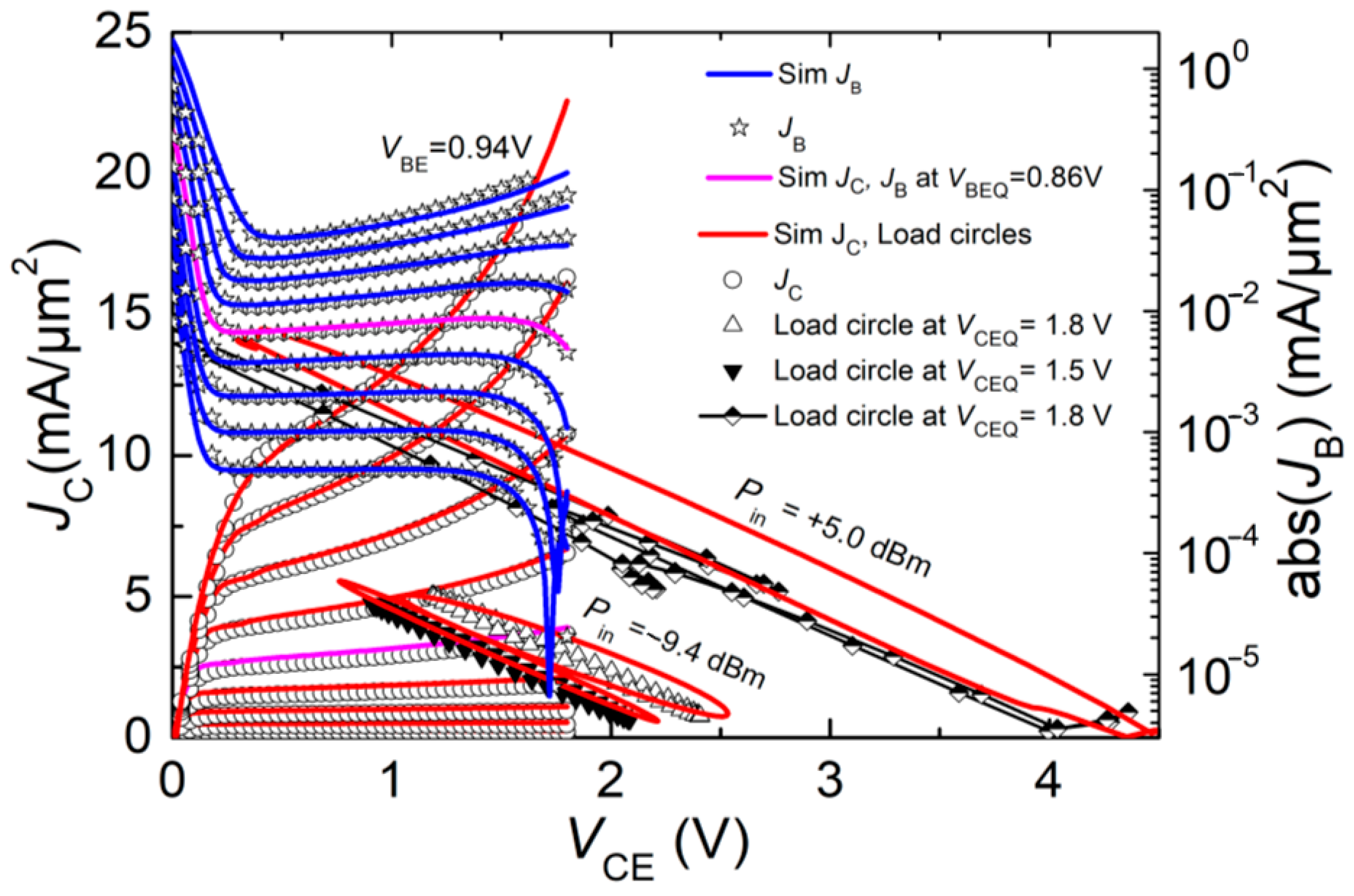
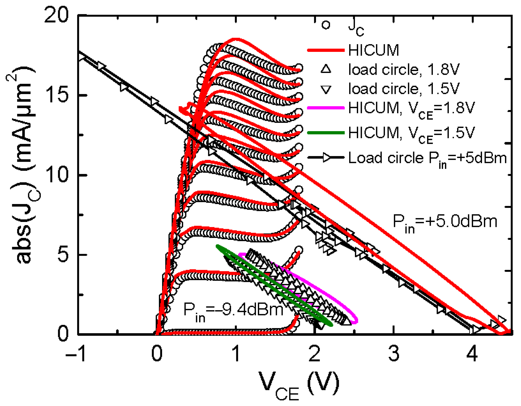
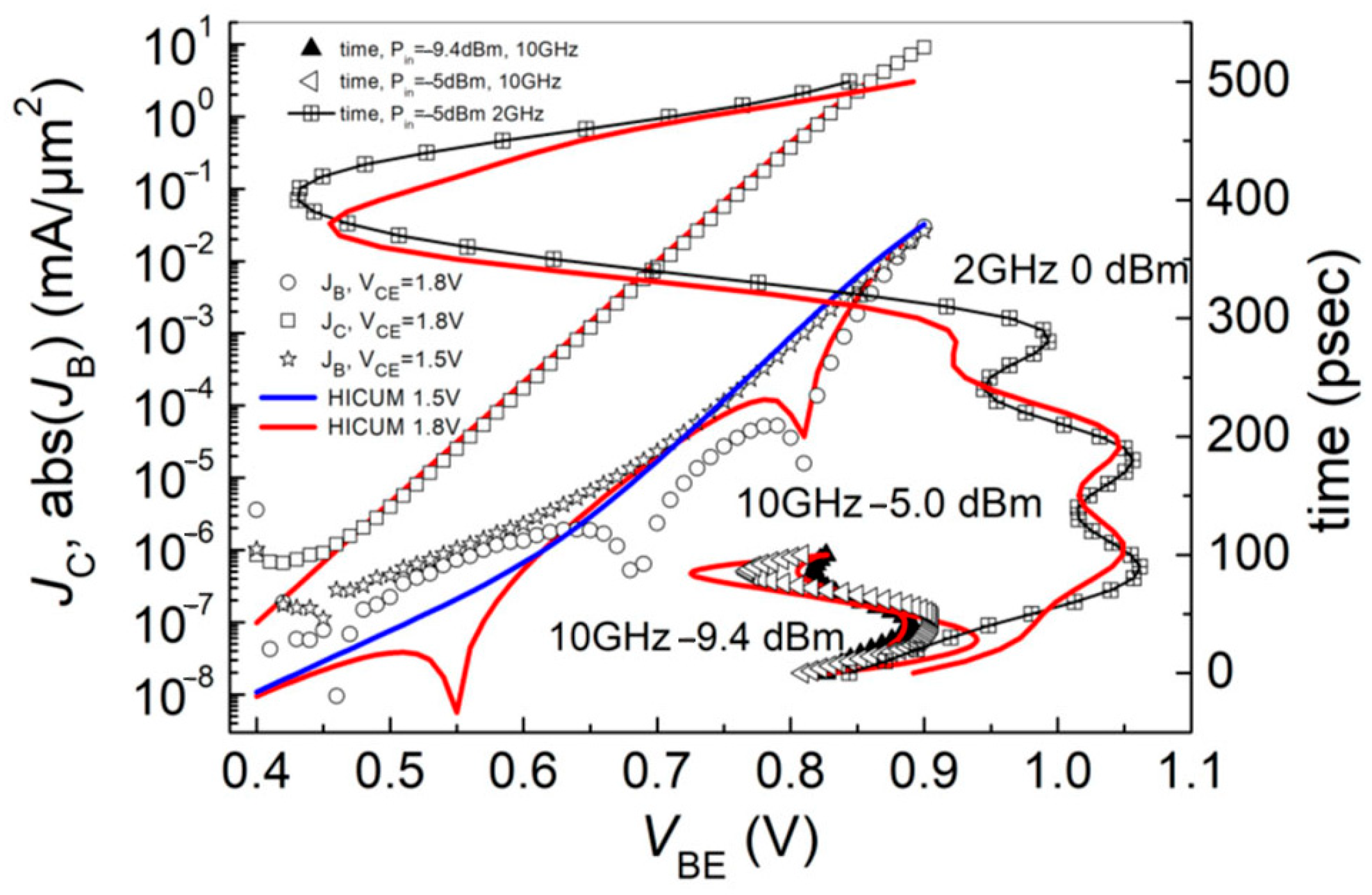
3.1. DC and RF Characteristics

The current–voltage output characteristics, JC (VCE) driven by VBE and IB, for the power cell are shown in Figure 5 and Figure 6, respectively. Avalanche carrier multiplication is observed, leading to a negative base current with a threshold voltage at VBE = 0.74 V, corresponding to a breakdown voltage BVCE0 = 1.7 V (see Figure 5). Additionally, the load circles at incident RF power levels Pin = −9.4 and +5 dBm at a fundamental frequency of 10 GHz are presented in both figures. It is important to note that the quiescent JC (VCE) and JB (VCE) characteristics shown in both plots do not include dynamic currents associated with incident RF power. The superimposed load circles indicate the range of the current swing under RF excitation.
Compact model simulations (shown as lines) exhibit good agreement with experimental data. At an RF input power of +5 dBm, the load circles become significantly distorted, reflecting nonlinear behavior and dynamic load modulation effects. The nonlinear dynamic collector–emitter voltage VCEd swing exceeds the breakdown voltage BVCE0, indicating that nonlinearities associated with impact ionization (I.I.) currents may contribute to harmonic distortion (HD). Nevertheless, the choice of a relatively high VCE0 = 1.8 V remains advantageous for power circuit applications [5,30,31], provided that the input power is not excessively high. Although the compact model shows better agreement with measured data at lower frequencies (e.g., 2 and 5 GHz), a higher RF frequency of 10 GHz was deliberately selected to enable analysis of the peculiar behavior of the third harmonic in high-frequency SiGe HBT power cells (PwCs).
The Gummel plot at VCE = 1.5 and 1.8 V is shown in Figure 7. The observed dips in the absolute values of base current density JB values at VCE = 1.8 V are attributed to avalanche multiplication currents occurring in the base–collector junction. The dynamic base–emitter voltage waveforms VBEd, induced by the incident RF input power, extend into the nonlinear region of the static JC (VBE) and JB (VBE) characteristics, thereby triggering nonlinearity in the transconductance. This nonlinear behavior is frequency-dependent and may also be influenced by the nonlinear behavior of the input capacitance Cin. It is important to note that JC shown in Figure 7 does not account for the superposition of the dynamic RF currents. The dynamic VBEd waveforms in the time domain at 2 and 10 GHz serve to illustrate the extent of bias swing within the static quiescent bias scale under high input power excitation. The collector’s current cut-off frequency fT and maximum oscillation frequency fmax as a function of JC are presented in Figure 8. At 2 GHz and an input power Pin = 0 dBm, the dynamic current density wave becomes distorted (flattened) and reaches the JC level corresponding to the peak fT. The ripples in the current waves stem from a too-low harmonic number (5), while Fourier transformation is applied for the signal conversion from the frequency to the time domain. High input RF power waves, especially at lower frequencies, face limitations because of nonlinearity in the transconductance.
Measured total collector (JC), and base current (JB) densities (including both static and dynamic components) as a function of incident RF power are presented in Figure 9 and Figure 10. For Pin = −15 dBm at VCE = 1 V, the frequency-dependent JC and JB increase with Pin. At lower frequencies, the increases in JC (Pin) and JB (Pin) are more pronounced, suggesting a capacitive origin of the nonlinear dynamic current. At VCE = 1.8 V, impact ionization (I.I.) additionally occurs and contributes positively to the total collector current density (JC + JCd), as shown in Figure 9 (red curve, Delta JC). This term represents the current component arising from I.I. and includes a minor contribution from self-heating effects (cf. the pink line in Figure 5, which shows only a slight increase with VCE).
The complete (quiescent and dynamic) frequency-dependent base current densities JB (Pin) at VCE = 1 V and 1.8 V are depicted in Figure 10. The frequency dependence of both JC and JB at both VCE values is attributed to the junction diffusion and substrate capacitances. At higher incident powers and elevated electric fields (i.e., VCE = 1.8 V) hot electrons in the base–collector (BC) region undergoes impact ionization, leading to a negative contribution to the base current, as seen in the JB (Pin) behavior in Figure 10. The impact-ionization-induced current and the nonlinear dynamic current act in opposition: while the I.I.-related current reduces JB, potentially turning it negative, the nonlinear dynamic current increases with Pin, driving JB toward positive values. At lower frequencies (f = 2 and 5 GHz), the nonlinear component of the base current contribution is more pronounced and counteracts the impact ionization (I.I.) component in JB (Pin), as shown in Figure 10. At VCE = 1.8 V, the initially negative base current density JB becomes positive once the incident power Pin exceeds the frequency-dependent threshold. This transition indicates the emergence of a nonlinear dynamic current that competes with the impact ionization (I.I.) contribution and includes a component due to self-heating effects (cf. Figure 10). The dynamic collector current component remains positive across all conditions, as does the I.I. contribution to the collector current.
The frequency-dependent nonlinear current is also influenced by the base–emitter bias: increasing VBE enhances the I.I. current. Accordingly, the base current density, resulting from impact ionization, becomes more pronounced at higher VBE values, as shown in Figure 11.
The dynamic base–emitter voltage (VBEd) at VCE = 1 V (I.I. free) exhibits a dependence on the input power, as shown in Figure 12. At higher VBE and at frequency of 10 GHz, the VBEd contribution is less pronounced.
The dependence of dynamic base–emitter voltage VBEd at the fundamental frequency of 10 GHz on Pin, measured at VCE = 1.8 V (including I.I.), is shown on a logarithmic scale. The dynamic VBEd (Vin in Figure 13) exhibits highly linear behavior with respect to Pin, with no significant increase in the third-harmonic component of VBEd beyond the input power of interest (−8 dBm). This suggests that the observed rise in the third-harmonic power is not attributed to the input capacitance.
Rapid increase in the third harmonic of the total output voltage Vout (VCEd) is observed in the Vout (Pin) dependence, as shown in Figure 14. This effect is frequency-dependent and appears for the fundamental incident frequencies between 10 GHz and 12 GHz. A similar drop-out of the third-harmonic power was also seen in B11HFC process technology of SiGe HBT power cells [32] (cf. Figure 15). This indicates that the effect is systematic and cannot be attributed to specific technological process variations. The same measurement setup was used to characterize other standard SiGe power transistors as well as InP HBTs, and no such drop-out was observed in those devices. We therefore hypothesize that the effect originates from reactive components in the transistor’s output structure, particularly in the base–collector p-n junction capacitance CBC and/or substrate–collector capacitance CSC, and nonlinearity of diffusion capacitances.
Although standard compact model (CM) simulations, including EM-simulated parasitic capacitances of the transistor’s metal interconnects, show good agreement with the measured results, they do not capture the observed third-harmonic behavior. Specifically, the resonance is not due to parasitic capacitances of the metallic routing. Data analysis shows that the drop-out of the third-harmonic power is not related to I.I. current since it occurs for both VCE = 1 V and 1.8 V.
In the next section, an analysis of the capacitance behavior under RF power at different frequencies is given.

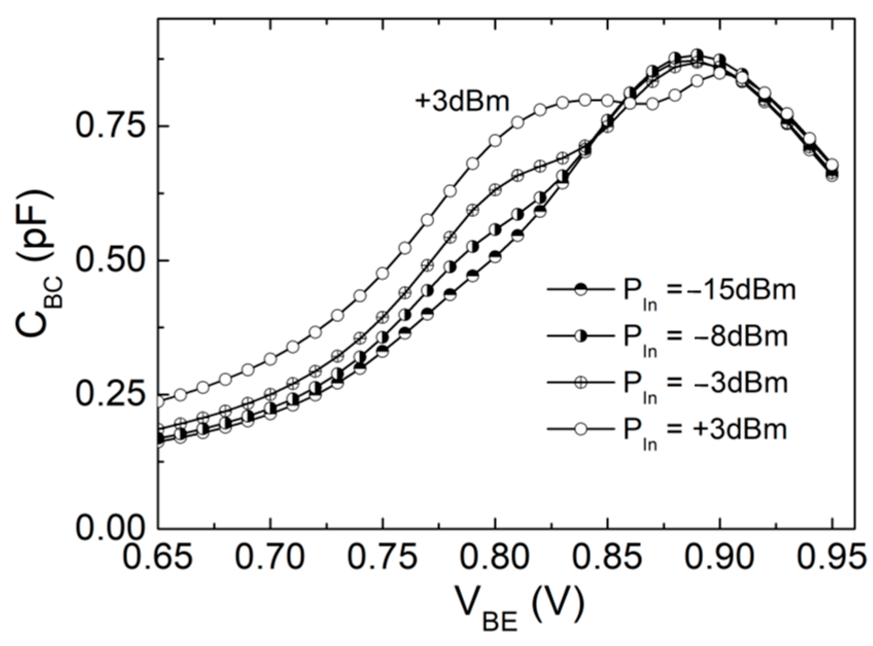
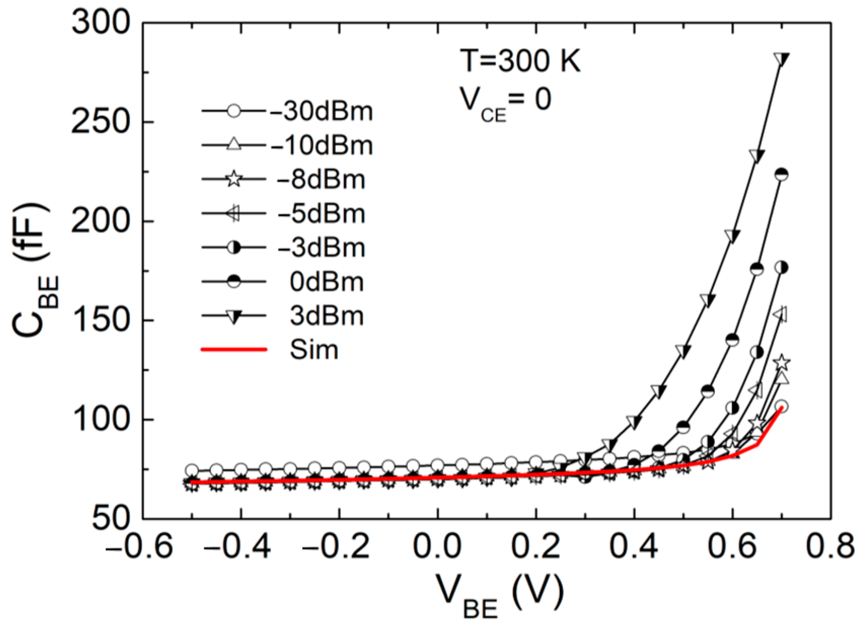
3.2. Dynamic Behavior of the Diffusion Capacitances

At a lower RF input power (Pin = −9.4 dBm), simulated collector current density shows agreement with the measured data, as evidenced by the load lines in Figure 5 and Figure 6. However, at higher input powers (Pin > −8.4 dBm), the dynamic current behavior is influenced by multiple nonlinear mechanisms: nonlinear transconductance, the nonlinearity due to diffusion capacitances, impact ionization currents, and the self-heating effect. It is known that avalanche current creates traps in the emitter–base region, particularly within the shallow trench isolation of the HBT. In the shallow trench of the HBT, an increase in the substrate capacitance CSC was observed [30].
To investigate the impact of incident RF power on the SiGe HBTs, capacitance measurements and extractions were performed at different incident RF power levels, as shown in Figure 16, Figure 17, Figure 18, Figure 19 and Figure 20. The base–collector and base–emitter junction capacitances were extracted from measured S-parameters. Such extraction is valid unless there is no gain in the DUT. As shown in Figure 16, the base–emitter junction capacitance CBE increases with VBE, as expected. However, under certain conditions (Pin = −5 dBm), CSC becomes significantly negative (−150 fF). A negative substrate capacitance can be interpreted as an inductive behavior, which may give rise to dynamic current resonance, at the corresponding frequency—a phenomenon observed in Figure 14, where a third harmonic emerges for Pin > −8 dBm. The physical interpretation and implications of negative capacitance are discussed in detail in Section 3.3.
As shown in Figure 17, deviations of CBC from a uniform (homogeneous) increase begin to appear at Pin > −8 dBm. The non-uniform dependence of CBC (VBE) behavior indicates the presence of a harmonic distortion source.
The diffusion-related components of the junction capacitances—CBE, CBC, and particularly CSC—exhibit sensitivity to the incident RF power. During nonlinear harmonic measurements, incident power waves can reach levels as high as +5 dBm. At higher RF power levels, starting from approximately −8.4 dBm, the base–collector junction capacitance CBC displays non-uniform behavior with respect to input power, as illustrated in Figure 17.
CBE (VBE) behavior remains homogeneous over a wide range of input powers, as shown in Figure 18. Similarly, the harmonic component of the input voltage Vin (Pin) also exhibits a homogeneous response, as shown in Figure 13. Compact-model-based simulations performed at Pin = −30 dBm show excellent agreement with the measured data.
The dependence of the total (depletion and diffusion) base–collector junction capacitance on RF power and bias across the base–collector p–n junction VBC dependence for the PwC and single h. s. SiGe HBT are presented in Figure 19. The CM simulation at Pin = −30 dBm matches the measured data. The homogeneous CBC (VBC) increase with Pin does not imply any anomalies that could be associated with a rapid rise in third-harmonic power or dynamic resonance effects. The typical biasing range of the transistor VBC is between −0.5 to 0 V, cf. Figure 19. In this area, CBC is less RF-power-dependent. The substrate capacitance is quite sensitive to input RF power at positive VBC only, cf. Figure 20.
The usual biasing of the transistor is between VBC of [−1 to 0] V, where CSC(VBC) exhibits nearly linear behavior with minimal dependence on RF power. Simulated data partially captures CSC(VBC) reduction for positive VBC, but only at lower incident RF power levels, as shown in Figure 20.
The absence of a resonance at 30 GHz in single high-frequency SiGe HBTs is attributed to the substrate–collector capacitance CSC being significant smaller, compared to that of the PwC HBTs, in a single h. f. SiGe HBT (Figure 20) and negligible in AIIIBV HBTs. The expected resonance for a single SiGe HBT with more than 4 times smaller CSC capacitance may be shifted to a higher frequency. The resonance of the third harmonic power at 30 GHz was also found in a different technology [32] SiGe HBT PwC, cf. Figure 15.
The third-harmonic drop-out in an IFX device occurs at a lower Pin = −14 dBm, compared to the IHP technology, where the drop-out begins at Pin = −8.4 dBm.
The third harmonic drop-out in is not evident at this frequency for a PDK h. f. SiGe HBT (Figure 21) probably due to a smaller CSC value. The shape of the harmonic power P3 (Pin) dependence on a single h. f. SiGe HBT is similar to that of the PwC but with a less expressed increase beyond −10 dBm of Pin.
The measured Pout (Pin) at 10 GHz and the corresponding third harmonic at various ambient temperatures (Ta) are presented in Figure 22. It is clearly observed that the peculiar behavior of the third harmonic is not temperature dependent. This indicates that the nonlinearity of transconductance, which is very sensitive to Ta, is not the main reason for the peculiar behavior of the third harmonic. However, the threshold input power at which the nonlinear effect begins shifts to a higher Pin with a decrease in temperature.
What happens when high RF input power is applied? Pin with 2 and 10 GHz frequencies is applied to the SiGe PwC input. Using Fourier transformation, Pout was converted to the corresponding RF power waveforms. The extracted VBC waves were superimposed on the CSC (VBC), cf. Figure 23. It is seen that incident RF power-related dynamic VBC output waves can exceed quiescent VBC = 1 V, cf. Figure 23, and cause CSC (VBC) reduction down to negative values, consistent with observations in Figure 16.
Negative capacitance can introduce effective inductive behavior, potentially leading to resonance at specific frequencies within the circuit.

3.3. Understanding Negative Capacitance in the HBT

The frequency-dependent complex dielectric permittivity, εeff (ω) = ε′(ω) − i ε″(ω), or the corresponding complex capacitance, C (ω) = C′(ω) − i C″(ω), define the response of dielectric polarization to an alternating electric field or the stored charge to alternating voltage on a capacitor [33]. Usually ε′, ε″, C′, and C″ are positive, indicating that the polarization/charge is in phase with the driving field/voltage and energy losses are present due to dielectric relaxation. Negative values of ε″ and C″ are incompatible with a passive system; otherwise, that would create an energy gain from the polarization change, which violates the principles of energy conservation. The case of a negative real part, ε′ or C′, corresponds to a system in which the oscillations of polarization/charge are in antiphase with the driving field/voltage, and this is the case in resonant systems above the resonant frequency [33]. One possible situation raising negative charge in the system is the presence of two charge carrier species of opposite sign in a semi-insulating medium. If one charge, e.g., electrons, is injected as homo charge at the negative electrode, the current is limited by the resulting space charge, but this may be relieved by the arrival of the hetero charge of opposite polarity from the other electrode. The time delay to the onset of a rising current under these circumstances is determined by the transit time of the hetero charges across the sample [33]. Investigated SiGe power cells exhibited negative CSC versus VBE in the operating VBE range: 0.8 V to 0.92 V, cf. Figure 15.
Negative capacitance was also observed in the bipolar transistor, but without a proper physical explanation [34]. Indeed, in the SiGe HBT, the charge of the base/collector junction and the charge in the collector substrate corresponds to two charge species with opposite signs. This explains the negative charge in the SiGe HBT. Alternating high-frequency power inserted from the RF (the source of the Vector Network Analyzer) source stays in phase with QBE dynamic charge but is in antiphase to the other, QSC, charge, thus releasing it. This implies a rise in the substrate dynamic frequency-dependent current and results in a significant increase in harmonic distortion.
The case of a negative real part, ε′ or C′, corresponds to a system in which the oscillations of polarization/charge are in antiphase with the driving field/voltage, and this is the case in resonant systems above the resonant frequency. The electrical lumped component representation involves an inductance L that necessarily implies the existence of magnetic energy storage in the system, which may not always be physically plausible. A series electrical circuit consisting of resistance R and inductance L may be represented, in the limit of high frequencies, ω >> R/L, by an effective capacitance Ceff = −l/ω2L that has the required negative sign but also has the specific inverse quadratic frequency dependence. Genuine inductive behavior requires, therefore, that the observed ‘negative capacitance’ should be seen at ‘high’ frequencies, that it should have a physical explanation, involving magnetic storage of energy, and that its frequency dependence should be l/ω2L [35].

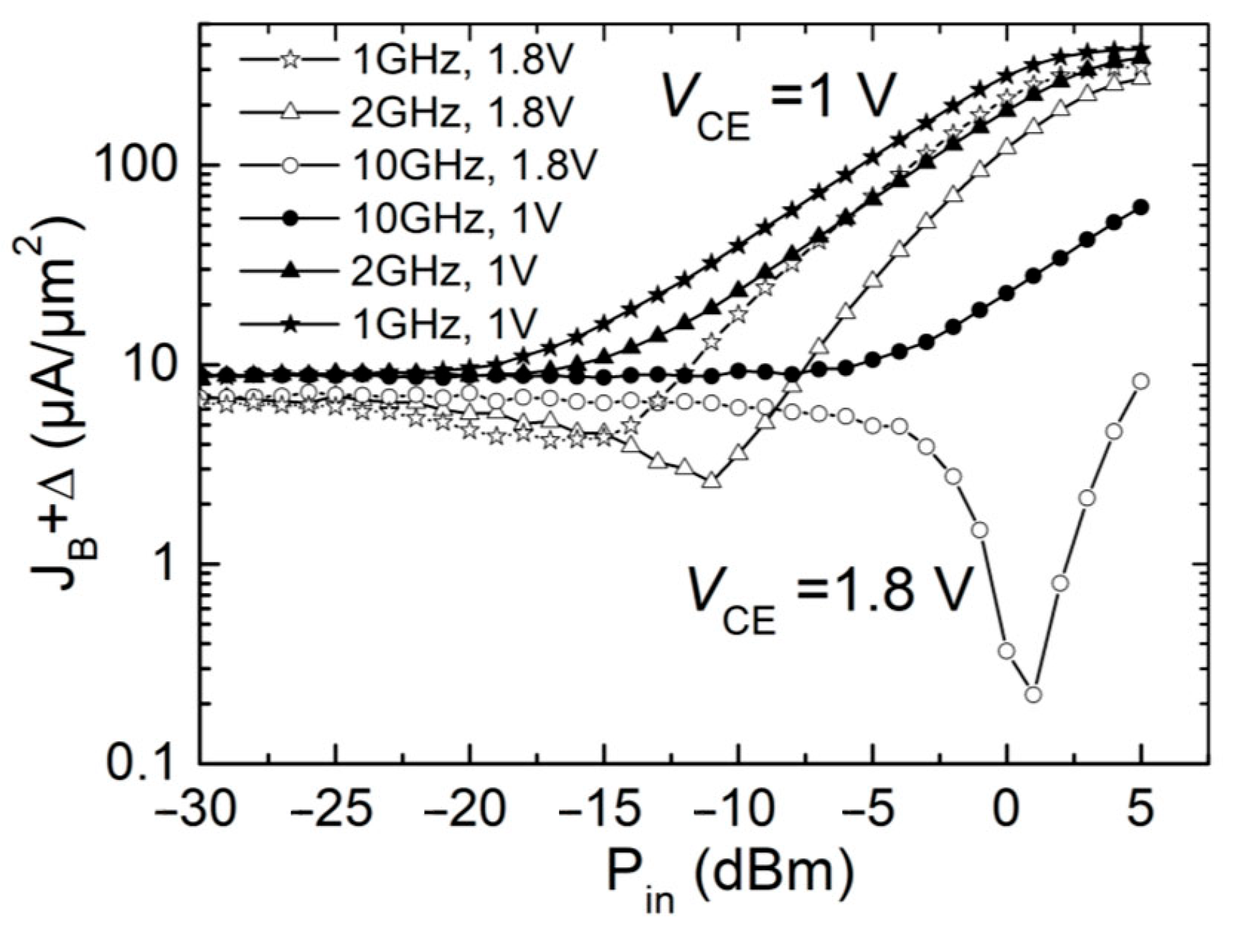
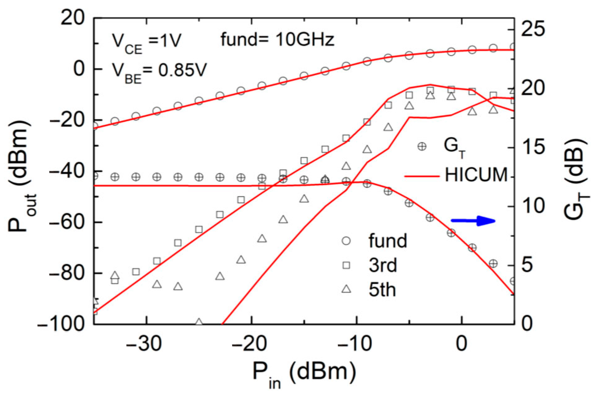
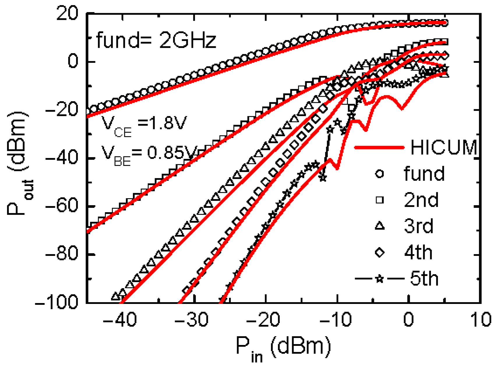
3.4. Power Characteristics of CE Power Cell, Discussion

The investigated devices yield high fT/fmax (250/220 GHz), cf. Figure 8, and acceptable power linearity up to moderate input powers of Pin = −5 dBm (Figure 24 and Figure 25). The compact model accounts for most of the nonlinearity sources in SiGe HBT PwCs, except for the odd behavior of the third harmonic. In general, there are six known main sources of distortion in SiGe HBTs, related to IB (VBE), ICE (VBE,VBC), ICB (VBE,VCB), CBC (VBC), CBE (VBE), and CSC (VSC) [16,17,18,36]. Following nonlinear measurement data analysis, the dominant power transfer through the HBT nonlinearity source up to −5 dBm of input power in the investigated SiGe PwCs is related to transconductance nonlinearity.
The power of the third harmonic shows a sharp increase beyond Pin > −13 dBm for Infineon technology [32] PwCs and −8.4 dBm for IHP technology [26] PwCs at a 30 GHz frequency, cf. Figure 15 and Figure 24. Data analysis shows that the drop-out of the third harmonic is related to the peculiarities of the substrate capacitance. This behavior is frequency-dependent and is observable only for SiGe power cells at fundamental frequency of around 10 GHz (not present at 2 GHz, cf. Figure 25). Large signal measurements at cryogenic and elevated temperatures (Ta = 4.2 K–400 K) show that the peak of rapid increase in the third harmonic does not depend on Ta and on VCE in a reasonable range.
Let us consider avalanche-current-related nonlinearity. At VCE = 1.5 V, avalanche current in JB (Figure 7: stars and blue line) is not present, but an increase in the third-harmonic power is evident, cf. Figure 24. The avalanche multiplication factor (M-1) decreases with JC, resulting in a decrease in related nonlinearity with the collector current density [18]. At the input powers, beyond Pin = −8.4 dBm, where the third harmonic drops out (Figure 24), the current density is approximately JC = 2.8 mA/µm2 for VCE = 1.8 V, 10 GHz. This point fits the JC value at the peak fT. At such high saturation of the DC current density, the thermal heating is set on with an ambient temperature (simulated value: Ta = 393 K), which reduces impact ionization itself [37]. The dynamic current gives rise to additional heating, especially for parallel power cell devices, where the heat interaction between them is significant. Therefore, at such high JC values, avalanche-multiplication-current-related nonlinearity cannot dominate. Avalanche multiplication current’s contribution to nonlinearity itself is not responsible for the sharp increase in the third-harmonic power. On the other hand, avalanche multiplication current causes the device to degrade. Generated hot carriers in the base–collector space charge region (SCR) travel to the emitter–base and base–collector dielectric and damage the emitter–base and collector–base dielectric, creating traps in the shallow trench [30]. As a result, the base current degrades [35,38,39]. It was found that large voltage swings, even at low VCE, where avalanche is not present, degrade the base current. The observed effect is frequency-dependent: for 1, 2, and 5 GHz, the third harmonic does not show such a sharp increase and perfectly fits the model, cf. Figure 25, indicating that the observed effect is related to the charge, is not dependent on VCE, and finally, is not due to the systematic error. The observed dips in the harmonic powers are due to the cancellation effect, which was well explained with the transfer function and third-order derivative of input voltage swing [40]. An increase in the third harmonic power has the threshold origin: it moves toward lower Pin with an increase in quiescent bias VBE, cf. Figure 26. The input power generated by dynamic VBEd compensates quiescent VBE to maintain the threshold power.
An evaluation of the summarized threshold bias VBEΣ = VBE + VBEd from the measured power characteristics at 10 GHz of fundamental excitation yields an average threshold bias value of VBEΣ = 0.88 V (from 0.86 V to 0.9 V). To reveal the possible contribution of CBC (VBC), CBE (VBE), and CSC (VSC) nonlinearities, the bias dependencies of CBC and CBE are presented in Figure 23 and Figure 27. In the measured devices, the VBC swings with incident powers of −8.4 dBm and −5 dBm did not reach the strong nonlinear region of the CBC (VBC), cf. Figure 23. The selected bias point at VCE = 1.8 V pushes incident wave away from the CBC strong nonlinearity bias area (VBC > 0.25 V), thus disabling the harmonic distortion source from the base–collector CBC and substrate capacitance CSC nonlinearities in favor of the transfer current nonlinearity, which was shown to be a significant one at higher VCE values and at moderate current densities [16,18,36,41]. Analysis of the input voltage wave of incident power beyond Pin > −9.4 dBm reveals that the voltage swing hits the nonlinear region of CBE bias dependency, cf. Figure 27, thus invoking the contribution of CBE nonlinearity to the total distortion.
Nevertheless, the nonlinearity contribution from CBE is negligible (cf. Figure 13) [24,36] compared to gm and transfer current nonlinearity stemming from the self-heating and accumulated charge in the collector at a high VBE.
To show the power capabilities of the investigated SiGe HBT PwC, scalar and vectorial load-pull measurements at 10, 30, and 50 GHz were performed. The high-speed power cell exhibited a transducer power gain of GT = 22/11 dB at 10/50 GHz, respectively. The load-matched output power compression depends on the frequency and is correlated with the base current, cf. Figure 28.

4. Conclusions

The harmonic distortion and load-pull behavior of high-frequency SiGe power cells were investigated. A frequency-dependent increase in the third harmonic of 10 GHz fundamental incident power was observed. This increase in P3 (Pin) exhibits a threshold-like origin and is not attributed to avalanche multiplication or to nonlinearities in base–collector junction capacitance CBC (VBC) behavior. The frequency-dependent drop-out of the third harmonic in the output power is linked to resonance effects, associated with negative-charge-behavior-related resonance behavior in the substrate capacitance Csc (Pin). This phenomenon was observed in SiGe HBTs fabricated with two different technologies, indicating that it is not technology specific. A detailed analysis confirms that impact ionization (I.I.) is not responsible for the unusual behavior of P3 (Pin). Furthermore, the effect persists in the SiGe HBT PwCs across a wide temperature range (Ta = 4.2 K–400 K), suggesting its robustness. The SiGe HBT h. f. power cell in matched load conditions exhibits good linearity beyond 30 GHz frequency and is suitable for power applications in the V- and W-bands.

Author Contributions

P.S. did all the measurements, compact model parameter model extraction, large signal measurements, including cryogenic and all simulations. A.M. designed power cells, including layout optimization with EM tool and participated writing paper. All authors have read and agreed to the published version of the manuscript.

Funding

This work was supported by EU project TARANTO (H2020-ECSEL-2016-1-RIA-two-stage).

Data Availability Statement

Dataset available on request from the authors.

Acknowledgments

M. Schroter is acknowledged for CEDIC laboratory access and valuable discussions. Automatisierungs Technik Voigt GmbH is acknowledged for access to Laboratory 1. The authors are thankful to V. Mallet from MPI Corporation, A. Beraro, and A. Weam from Focus Microwaves for support and consulting. Rohde & Schwarz is acknowledged for its support with equipment.

Conflicts of Interest

Author Paulius Sakalas was employed by the company BPTI Baltic Institute of Advanced Technology and MPI Corporation, author Anindya Mukherjee was employed by the company Infineon Technologies AG. The remaining authors declare that the research was conducted in the absence of any commercial or financial relationships that could be construed as a potential conflict of interest.

References

  1. Schröter, M.; Wedel, G.; Heinemann, B.; Jungemann, C.; Krause, J.; Chevalier, P.; Chantre, A. Physical and Electrical Performance Limits of High-Speed SiGeC HBTs, Part I: Vertical Scaling. IEEE Trans. Electron Devices 2011, 58, 3687–3696. [Google Scholar] [CrossRef]
  2. Lachner, R. Towards 0.7 terahertz Silicon Germanium heterojunction bipolar technology–The DOTSEVEN project. ECS Trans. 2014, 64, 21–37. [Google Scholar] [CrossRef]
  3. Fox, A.; Heinemann, B.; Rucker, H.; Barth, R.; Fischer, G.G.; Wipf, C.; Marschmeyer, S.; Aufinger, K.; Bock, J.; Boguth, S.; et al. Advanced Heterojunction Bipolar Transistor for Half-THz SiGe BiCMOS Technology. IEEE Electron Device Lett. 2015, 36, 642–644. [Google Scholar] [CrossRef]
  4. Yoon, D.; Kim, J.; Yun, J.; Kaynak, M.; Tillack, B.; Rieh, J.-S. 300-GHz Direkt and Heterodyne Active Imagers Based on 0.13-μm SiGe HBT Technology. IEEE Trans. Terahertz Sci. Technol. 2017, 7, 536–545. [Google Scholar] [CrossRef]
  5. Yishay, R.B.; Carmon, R.; Katz, O.; Elad, D. Correct. In Proceedings of the 2010 IEEE Radio Frequency Integrated Circuits Symposium, Anaheim, CA, USA, 23–25 May 2010; pp. 529–532. [Google Scholar]
  6. Cilici, F.; Margalef-Rovira, M.; Lauga-Larroze, E.; Bourdel, S.; Leger, G.; Vincent, L.; Mir, S.; Barragan, M.J. Nonintrusive Machine Learning-Based Yield Recovery and Performance Recentering for mm-Wave Power Amplifiers: A Two-Stage Class-A Power Amplifier Case Study. IEEE Trans. Microw. Theory Tech. 2023, 72, 3046–3064. [Google Scholar] [CrossRef]
  7. Thian, M.; Tiebout, M.; Buchanan, N.B.; Fusco, V.F.; Dielacher, F. A 76-84 GHz SiGe Power Amplifier Array Employing Low-Loss Four-way Differential Combining Transformer. IEEE Trans. Microw. Theory Tech. 2013, 61, 931–938. [Google Scholar] [CrossRef]
  8. Floyd, B.A.; Reynolds, S.; Pfeiffer, U.; Zwick, T.; Beukema, T.; Gaucher, B. SiGe Bipolar Transciever Circuits Operating at 60 GHz. IEEE J. Solid-State Circuits 2005, 40, 156–167. [Google Scholar] [CrossRef]
  9. Lin, C.-H.; Su, Y.-K.; Juang, Y.-Z.; Chiu, C.-F.; Chang, S.-J.; Chen, J.F.; Tu, C.-H. The Optimized Geometry of the SiGe HBT Power Cell for 802.11 a WLAN Applications. IEEE Microw. Wirel. Compon. Lett. 2007, 17, 49–51. [Google Scholar] [CrossRef]
  10. Wu, K.; Fahs, B.; Hella, M. A 220 GHz Outphasing Transmitter in 130-nm BiCMOS Technology. In Proceedings of the 2018 IEEE BiCMOS and Compound Semiconductor Integrated Circuits and Technology Symposium (BCICTS), San Diego, CA, USA, 15–17 October 2018; pp. 227–230. [Google Scholar]
  11. Chang, M.; Rebeiz, G.M. A Wideband High-Efficiency 79-97 GHz SiGe Linear Power Amplifier with >90 mW Output. In Proceedings of the 2008 IEEE Bipolar/BiCMOS Circuits and Technology Meeting, Monterey, CA, USA, 13–15 October 2008; pp. 69–72. [Google Scholar]
  12. Sakalas, M.; Joram, N.; Ellinger, F. Fully Differential High Input Power Handling Ultra-Wideband Low Noise Amplifier for MIMO Radar Application. In Proceedings of the 2017 IEEE Compound Semiconductor Integrated Circuit Symposium (CSICS), Miami, FL, USA, 22–25 October 2017. [Google Scholar]
  13. Datta, K.; Hashemi, H. Performance Limits, Design and Implementation of Class-E mm-Wave SiGe HBT Class-E and Stacked Power Amplifiers. IEEE J. Solid-State Circuits 2014, 49, 2150–2170. [Google Scholar] [CrossRef]
  14. Ma, Z.; Jiang, N. Base-Region Optimization of SiGe HBTs for High-Frequency Microwave Power Amplification. IEEE Trans. Electron Devices 2006, 53, 875–883. [Google Scholar]
  15. Gu, Q.J.; Xu, Z.; Chang, M.-C.F. Two-Way Current-Combining W-Band Power Amplifier in 65-nm CMOS. IEEE Trans. Microw. Theory Tech. 2012, 60, 1365–1374. [Google Scholar] [CrossRef]
  16. Yuan, X.; Lie, D.; Larson, L.; Blonski, J.; Gross, J.; Kumar, M.; Mecke, J.; Senior, A.; Chen, Y.; Poh, A.; et al. RF linearity study of SiGe HBTs for Low Power RFIC Design, Part 1. In Proceedings of the 2002 3rd International Conference on Microwave and Millimeter Wave Technology, 2002, Proceedings, ICMMT 2002, Beijing, China, 17–19 August 2002; pp. 70–73. [Google Scholar]
  17. Wambacq, P. Distortion Analysis of Analog Integrated Circuits; Klüver Academic Publishers: Dordrecht, The Netherlands, 1998. [Google Scholar]
  18. Niu, G.; Liang, Q.; Cressler, J.; Webster, C.; Harame, D. RF Linearity Characteristics of SiGe HBT. IEEE Trans. Microw. Theory Tech. 2000, 49, 1558–1565. [Google Scholar]
  19. Kracht, J.; Loffler, B.; Ribic, N.; Wachmann, E. BVCE0-Increased Operating Voltage for SiGe HBTs. In Proceedings of the 2006 IEEE International Reliability Physics Symposium Proceedings, San Jose, CA, USA, 26–30 March 2006; pp. 507–511. [Google Scholar]
  20. Sakalas, P.; Mukherjee, A.; Schroter, M. Distortion Analysis of CE and CB SiGe HBT Power-Cells with fmax beyond 220 GHz for Millimeter-Wave Applications. In Proceedings of the 2019 IEEE BiCMOS and Compound Semiconductor Integrated Circuits and Technology Symposium (BCICTS), Nashville, TN, USA, 3–6 November 2019; pp. 1–4. [Google Scholar]
  21. Schroter, M.; Pehlke, D.; Lee, T.-Y. Compact Modeling of High-Frequency Distortion in Silicon Integrated Bipolar Transistors. IEEE Trans. Electron Devices 2000, 47, 1529–1535. [Google Scholar] [CrossRef]
  22. de Vreede, L.C.N.; de Graaff, H.; Mouthaan, K.; de Kok, M.; Tauritz, J.; Baets, R. Advanced Modeling of Distortion effects in Bipolar Transistors using the Mextram Model. IEEE J. Solid-State Circuits 1996, 31, 114–121. [Google Scholar] [CrossRef]
  23. Sansen, W. Distortion in Elementary Transistor Circuits. IEEE Trans. Circuits Syst.-II Analog. Digit. Signal Process. 1999, 46, 315–325. [Google Scholar] [CrossRef]
  24. Samelis, A.; Pavlidis, D. Mechanisms Determining Third Order Intermodulation in AlGaAs/GaAs Heterojunction Bipolar Transistors. IEEE-Trans. Microw. Theory Tech. 1992, 40, 2374–2380. [Google Scholar] [CrossRef]
  25. Wambacq, P.; Gielen, G.G.; Kinget, P.R.; Sansen, W. High-Frequency Distortion Analysis of Analog Integrated Circuits. IEEE Trans. Circuits Syst. II Analog. Digit. Signal Process. 1999, 46, 335–345. [Google Scholar] [CrossRef]
  26. Heinemann, B.; Barth, R.; Bolze, D.; Drews, J.; Fischer, G.G.; Fox, A.; Fursenko, O.; Grabolla, T.; Haak, U.; Knoll, D.; et al. SiGe HBT Technology with fT/fmax of 300 GHz/500 GHz and 2.0 ps CML Gate Delay. In Proceedings of the 2010 International Electron Devices Meeting, San Francisco, CA, USA, 6–8 December 2010; pp. 688–691. [Google Scholar]
  27. Schetzen, M. The Volterra and Wiener Theories of Nonlinear Systems; Wiley: New York, NY, USA, 1980. [Google Scholar]
  28. Van Moer, M.; Rolain, Y. A Large-Signal Network Analyzer: Why is it needed? IEEE Microw. Mag. 2006, 7, 46–62. [Google Scholar] [CrossRef]
  29. Sakalas, P. Focus Application Note. AN-67, Vectorial Harmonic Load Pull for mm-Wave Frequency Power Device Characterization and Compact Model Verification. Available online: https://focus-microwaves.com/wp-content/uploads/2024/06/20221114-Vectorial-Load-Pull-for-mm-Wave-Frequency-Power-Device-Characterization-and-Compact-Model-Verification-MPI.pdf (accessed on 30 June 2025).
  30. Grens, C.M.; Cheng, P.; Cressler, J.D. Reliability of SiGe HBTs for Power Amplifiers–Part I: Large-signal RF Performance and Operating Limits. IEEE-Trans. Device Mater. Reliab. 2009, 9, 431–439. [Google Scholar] [CrossRef]
  31. Cheng, P.; Grens, C.M.; Cressler, J.D. Reliability of SiGe HBTs for Power Amplifiers–Part II: Underlying Physics and Damage Modeling. IEEE-Trans. Device Mater. Reliab. 2009, 9, 440–448. [Google Scholar] [CrossRef]
  32. Dielacher, F.; Tiebout, M.; Lachner, R.; Knapp, H.; Aufinger, K.; Sansen, W. SiGe BiCMOS Technology and Circuits for Active Safety Systems. In Proceedings of the Technical Papers of 2014 International Symposium on VLSI Design, Automation and Test, Hsinchu, Taiwan, 28–30 April 2014; pp. 1–4. [Google Scholar]
  33. Jonscher, A.K. The Physical Origin of Negative Capacitance. J. Chem. Soc. Faraday Trans. 2 Mol. Chem. Phys. 1986, 82, 75–81. [Google Scholar] [CrossRef]
  34. Maseko, N.S. Negative Capacitance Analysis of Discrete Semiconductors. Ph.D. Thesis, University of Johannesburg, Johannesburg, South Africa. Available online: https://ujcontent.uj.ac.za/esploro/outputs/graduate/Negative-capacitance-analysis-of-discrete-semiconductors/9930309107691 (accessed on 22 August 2017).
  35. Freeman, G.; Rieh, J.-S.; Yang, Z.; Guarin, F. Reliability and performance scaling of very high speed SiGe HBTs. Microelectron. Reliab. 2004, 44, 397–410. [Google Scholar] [CrossRef]
  36. Niu, G.; Liang, Q.; Cressler, J.; Webster, C.; Harame, D. Systematic Analysis of RF Distortion in SiGe HBT’s. In Proceedings of the 2001 IEEE Radio Frequency Integrated Circuits (RFIC) Symposium (IEEE Cat. No.01CH37173), Phoenix, AZ, USA, 20–22 May 2001; pp. 147–150. [Google Scholar]
  37. Sakalas, P.; Ramonas, M.; Schroter, M.; Jungemann, C.; Shimukovitch, A.; Kraus, W. Impact Ionization Noise in SiGe HBTs: Comparison of Device and Compact Modeling with Experimental Results. IEEE-Trans. Electron Devices 2009, 56, 328–336. [Google Scholar] [CrossRef]
  38. Grens, C.M.; Seth, S.; Cressler, J.D. Common-Base intermodulation Characteristics of advanced SiGe HBTs. In Proceedings of the 2008 IEEE Bipolar/BiCMOS Circuits and Technology Meeting, Monterey, CA, USA, 13–15 October 2008; pp. 244–247. [Google Scholar]
  39. Zhu, C.; Liang, Q.; Al-Huq, R.; Cressler, J.; Lu, Y.; Chen, T.; Joseph, A.; Niu, G. Damage Mechanisms in Impact-Ionization-Induced mixed-Mode Reliability Degradation of SiGe HBTs. IEEE Trans. Device Mater. Reliab. 2005, 5, 142–149. [Google Scholar]
  40. Lee, C.-P.; Ma, W.; Wang, N.L. Averaging and Cancellation Effect of High-Order Nonlinearity of a Power Amplifier. IEEE Trans. Circuits Syst.-I Regul. Pap. 2007, 54, 2733–2740. [Google Scholar]
  41. Lee, C.I.; Lin, Y.T.; Lin, W.C. Investigation of linearity in the high electric field region for SiGe HBTs based on Volterra series. IEEE Trans. Device Mater. Reliab. 2014, 14, 1049–1055. [Google Scholar] [CrossRef]
Figure 1. The top view of the SiGe PwC layout 2xCBEBEBC, where “E” is emitter, “B” in base and “C” is collector.
Electronics 14 02984 g001
Figure 2. Photos of two realizations of SiGe power cells with AE0 = 0.13 µm × 10.16 µm × 2 and contact CBEBEBC configuration, embedded in test structures: (a) perpendicular and (b) parallel to base and collector access lines.
Electronics 14 02984 g002
Figure 3. Harmonic distortion measurement setup with Keysight PNA-X N5247A nonlinear network analyzer and SMU N6705C.
Electronics 14 02984 g003
Figure 4. Schematic of vectorial LP measurement system with Delta impedance tuners from Focus Microwaves, C-67100 at the source and harmonic tuner M-67100 at port 4. Incident to the DUT input power wave is b1 and reflected from the input of the DUT power wave is a1. Transferred through the DUT power wave is b2 and reflected from the DUT output wave is a2.
Electronics 14 02984 g004
Figure 5. Collector and base current density of the PwC versus VCE with VBE drive (0.74 to 0.94 V, 0.02 V step). Load circles are for quiescent VCEQ = 1.5 V and VCEQ = 1.8 V at 10 GHz.
Electronics 14 02984 g005
Figure 6. Collector current density versus VCE with IB drive: 1 µA to 501 µA with 50 µA step. Load circles are for VCE = 1.5 V and VCE = 1.8 V at 10 GHz.
Electronics 14 02984 g006
Figure 7. Gummel plot at VCE = 1.8 V and 1.5 V, input voltage waves with input powers Pin = −9.4 and −5 dBm at 10 GHz and 0 dBm at 2 GHz; lines are model data.
Electronics 14 02984 g007
Figure 8. fT and fmax over quiescent JC and collector dynamic current density swing at 2 and 10 GHz at VBE = 0.85 V, VCE = 1.5 V.
Electronics 14 02984 g008
Figure 9. Complete collector and base current densities versus Pin with different frequencies at VCE = 1 V and VBE = 0.85 V. Delta JC is JC at VCE = 1.8 V referenced to the static value of JC at VCE = 1 V.
Electronics 14 02984 g009
Figure 10. Frequency dependence of the JB versus Pin at different VCE values and VBE = 0.85 V. Δ = 1.5 µA/µm2 was used to avoid partially negative currents for logarithmic representation.
Electronics 14 02984 g010
Figure 11. Complete JB versus Pin at different VBE values at 10 GHz.
Electronics 14 02984 g011
Figure 12. Real and imaginary parts of dynamic VBEd versus Pin at different VBE values.
Electronics 14 02984 g012
Figure 13. Dynamic VBEd versus available power (Pin) at 10 GHz. VCE = 1.8 V and VBE = 0.85 V, symbols are measured, lines are simulated data.
Electronics 14 02984 g013
Figure 14. Collector dynamic voltage Vout versus RF input power Pin, symbols are measured, lines—simulated data. Blue stripe shows an input power threshold of the third harmonic drop-out.
Electronics 14 02984 g014
Figure 15. Pout (Pan) for IFX-technology B11HFC-process [32] SiGe HBT PwC, VCE = 1.5 V, VBE = 0.85 V, fundamental frequency: 10 GHz.
Electronics 14 02984 g015
Figure 16. Measured capacitances CBE and substrate capacitance CSC versus VBE at different CW powers and VCE = 0 V.
Electronics 14 02984 g016
Figure 17. Measured capacitance CBC versus VBE at different RF input powers and at VCE = 0 V.
Electronics 14 02984 g017
Figure 18. CBE versus VBE extracted from different CW powers, VCE = 0 V, red line is simulated data at Pin = −30 dBm.
Electronics 14 02984 g018
Figure 19. CBC versus VBC extracted from different CW powers, the red lines are CM for the PwC and single SiGe HBT.
Electronics 14 02984 g019
Figure 20. CSC versus VBC extracted from different CW powers for the SiGe PwC and the PDK HBT.
Electronics 14 02984 g020
Figure 21. Pout (Pin) of fundamental and harmonics for an h. s. single PDK SiGe HBT with CBE contact configuration from IHP-technology SG13G2 Process at 10 GHz, VCE = 1 V, and VBE = 0.85 V. Lines are simulated data. AE0 = 0.12 µm × 0.96 µm × 8. Blue arrow points to the GT axis.
Electronics 14 02984 g021
Figure 22. Pout (Pin) of the fundamental and the third harmonic for an h. s. PwC from IHP technology at 10 GHz; VCE = 1.0 V; and VBE = 0.85 V at 300 K, 0.875 V at 225 K, 1.025 V at 75 K, and 1.05 V at 20 K.
Electronics 14 02984 g022
Figure 23. Measured and modeled CBC and CSC versus VBC and superimposed dynamic VBC waves at 2 and 10 GHz frequencies.
Electronics 14 02984 g023
Figure 24. Output power of fundamental and harmonics versus input power for SiGe PwC from IHP technology [26] at 10 GHz, VCE = 1.5 V, and VCE = 1.8 V.
Electronics 14 02984 g024
Figure 25. Output powers of fundamental and harmonics versus input power at 2 GHz, VCE = 1.8 V.
Electronics 14 02984 g025
Figure 26. The Pout of the third harmonic versus Pin at different VBE values.
Electronics 14 02984 g026
Figure 27. Base–emitter capacitance versus VBE, and time-dependent dynamic VBEd at frequencies of 2 and 10 GHz at RF power of 0 dBm.
Electronics 14 02984 g027
Figure 28. Load-matched output RF power Pout and IB versus Pin at different frequencies measured with a scalar LP system. Red lines are simulated data.
Electronics 14 02984 g028
Disclaimer/Publisher’s Note: The statements, opinions and data contained in all publications are solely those of the individual author(s) and contributor(s) and not of MDPI and/or the editor(s). MDPI and/or the editor(s) disclaim responsibility for any injury to people or property resulting from any ideas, methods, instructions or products referred to in the content.

