Abstract
For data-intensive applications like edge AI and image processing, we present a new reconfigurable 8T SRAM-based in-memory computing (IMC) macro designed for high-performance and energy-efficient operation. This architecture mitigates von Neumann limitations through numerous major breakthroughs. We built a new architecture with an adjustable capacitance array to substantially increase the multiply-and-accumulate (MAC) engine’s accuracy. It achieves 10–20 TOPS/W and >95% accuracy for 4–10-bit operations and is robust across PVT changes. By supporting binary and ternary neural networks (BNN/TNN) with XNOR-and-accumulate logic, a dual-mode inference engine further expands capabilities. With sub-5 ns mode switching, it can achieve up to 30 TOPS/W efficiency and >97% accuracy. In-memory Hamming error correction is implemented directly using integrated XOR circuitry. This technique eliminates off-chip ECC with >99% error correction and >98% MAC accuracy. Machine learning-aided co-optimization ensures sense amplifier dependability. To ensure CMOS compatibility, the macro may perform Boolean logic operations using normal 8T SRAM cells. Comparative circuit-level simulations show a 31.54% energy efficiency boost and a 74.81% delay reduction over other SRAM-based IMC solutions. These improvements make our macro ideal for real-time AI acceleration, cryptography, and next-generation edge computing, enabling advanced compute-in-memory systems.
1. Introduction
In-memory computing (IMC) is a novel computational paradigm that addresses the constraints of conventional von Neumann systems by facilitating data processing directly within memory cells. The traditional division between processing and memory units leads to elevated data transfer costs, augmented latency, and considerable power consumption, commonly known as the von Neumann bottleneck. Arithmetic and Boolean operations are facilitated by the integration of computational circuits within memory units [1]. IMC mitigates these challenges by integrating computational functionalities within memory components, like DRAM [2] or SRAM [3], or novel non-volatile memories, like memristors [4]. By using IMC, computational efficiency is drastically improved, leading to enhanced speed, reduced power consumption, and greater parallelism [5].
Advancing memory technology is driving the evolution of in-memory computing (IMC), which mitigates the von Neumann bottleneck by facilitating processing within memory arrays. Memristors are distinguished by their non-volatility, rapid switching, analog state storing, and compatibility with crossbar topologies, rendering them ideal for vector-matrix multiplication, neuromorphic computing [6], and the acceleration of machine learning [7]. In contrast to conventional SRAM-based IMC, memristors provide enhanced energy efficiency, integrated density, and scalability, making them formidable contenders for next-generation computing platforms [8]. Recent studies highlight material improvements and system-level designs for memristor-based integrated memory computing, while advancements such as bio-voltage-operated peptide memristors demonstrate their potential in sensing and neuromorphic applications [9]. Additional developing memory chips, such as RRAM, PCM, and FeFETs, facilitate IMC by allowing storage and computation within a singular architecture. Nonetheless, the analog switching characteristics and synapse-like functioning of memristors offer significant benefits for the development of energy-efficient, high-density, and biologically inspired systems [10].
IMC can be classified into digital [11] and analog [12] computing as well as digital IMC executes bitwise logic operations, while analog IMC exploits the physical properties of memory devices for computations such as matrix-vector multiplications in AI accelerators. This technique is particularly relevant for modern applications in neuromorphic systems [13], cryptography [14], edge computing [15], and artificial intelligence (AI) [16], where high-speed, low-power computation is paramount. The direct implementation of fundamental Boolean gate operations within SRAM cells, which permits in-situ calculation without the need for data transfer to an external processing unit, is a significant development in IMC. SRAM-based IMC uses the electrical and structural properties of memory cells to carry out Boolean operations like AND, OR, XOR, and NOT, in contrast to conventional computing systems that depend on independent logic gates for basic operations. This removes needless data transportation, which cuts down on processing time and energy usage. By adjusting charge storage [17], bitline detection mechanisms [18], and word line activation procedures [19], logic operations may be carried out within memory cells, which makes SRAM-based IMC a scalable and effective method. SRAM-based IMC presents notable advantages over DRAM-based IMC owing to its enhanced speed, energy economy, and operational stability [20].
Despite DRAM’s superior storage capacity, SRAM is favored for latency-sensitive in-memory computing (IMC) owing to its expedited and more consistent access times (1–2 ns compared to 10–100 ns for DRAM), static data preservation, and absence of refresh cycles [21]. These characteristics render SRAM more energy-efficient and appropriate for real-time systems, such as UAVs and AI inference engines. Moreover, SRAM facilitates enhanced parallelism and bitwise operations, which are crucial for IMC workloads. Conversely, the row activation overhead and refresh demands of DRAM result in latency and energy inefficiencies, constraining its efficacy in performance-critical IMC applications.
Furthermore, SRAM’s CMOS architecture enables effortless integration with logic circuits and dedicated sense amplifiers, rendering it exceptionally appropriate for energy-efficient, high-performance IMC applications [22]. The application of Boolean logic in SRAM-based IMC encompasses many approaches that leverage the inherent properties of SRAM memory cells.
A prevalent method involves altering peripheral circuits, such as sensing amplifiers, to facilitate logic computations during read and write processes. Sense amplifiers can be engineered to identify particular logic states, facilitating operations such as NAND, NOR, and XOR directly within memory arrays. Another option is charge-sharing [23], which enables logic operations through regulated charge redistribution among bitlines. This approach minimizes switching energy while guaranteeing dependable computation. Moreover, selective activation approaches for word lines and bitlines facilitate in-memory logic execution by regulating the involvement of specific memory cells in calculations. This approach enables the simultaneous execution of numerous logic functions without necessitating significant architectural alterations to SRAM cells. The integration of these approaches improves computational efficiency, enabling SRAM-based IMC to execute intricate logic operations with minimal overhead. SRAM-based IMC provides significant advantages, rendering it a compelling solution for contemporary computing issues. This method dramatically lowers latency by avoiding frequent data transfers between memory and processors, resulting in accelerated processing times.
The intrinsic parallelism of SRAM-based IMC [24] facilitates the simultaneous execution of numerous logic operations across many memory cells, therefore enhancing throughput and computational density. Moreover, power consumption is significantly diminished as in-memory calculation obviates the necessity for specialized processing units, rendering SRAM-based IMC exceptionally energy-efficient. Utilizing advanced methods, including modified sense amplifiers, charge sharing, and selective word line/bitline activation, SRAM-based IMC facilitates highly efficient logic computing without significant architectural alterations.
This study introduces multiple innovative contributions that collectively enhance the state of the art in digital in-memory computing (IMC) for edge AI applications:
- Integrated Multi-Function IMC Macro: We provide the implementation of an 8T SRAM-based IMC macro that amalgamates configurable-precision MAC operations, digital Boolean logic, and single-error correction/double-error detection (ECC) within a cohesive multi-logic sense amplifier (MLSA). This co-integration facilitates functionally diverse and compact in-memory compute arrays without compromising performance or reliability.
- AI-Enhanced Design Space Exploration: We present an AI-driven framework to co-optimize hardware design parameters—such as sensing thresholds, transistor dimensions, and clock gating—maximizing sensing margin and energy efficiency amid process–voltage–temperature (PVT) changes. This methodology augments resilience and optimizes power-performance trade-offs.
- ECC-Aware Bit-Level Interleaving: To alleviate burst failures and improve fault tolerance, we devise a bit-interleaving method that spatially distributes adjacent data bits across memory banks. When connected with ECC, burst errors are converted into correctable single-bit errors, greatly enhancing data integrity.
These improvements facilitate low-latency, energy-efficient, and highly reliable IMC designs that are ideally suited for real-time, power-constrained edge computing applications.
The following is a summary of this study’s main contributions:
- Innovative 8T SRAM-based IMC Design: introduces an innovative 8T SRAM-based in-memory computing (IMC) design that employs standard 8T SRAM cells for CMOS compatibility and scalability, facilitating Boolean operations (NOR, OR, NAND, AND, XOR, and XNOR) with minimal alterations to read operations and peripheral circuits.
- Performance Enhancements: Confirmed using Monte Carlo simulations that consider process variations and voltage scaling, this design realizes a 74.81% reduction in latency and a 31.54% increase in energy efficiency compared to conventional SRAM-based IMC systems.
- Reduced Data Transfer: Minimizes the volume of data that needs to be transmitted, enhancing computational efficiency for applications employing real-time edge computing, cryptographic processors, and low-power AI accelerators.
- AI Workload Optimizations: Enhances suitability for AI tasks by proposing support for binary and ternary neural networks, time-domain computing, variable precision in transformer models, multi-bit MAC operations, and in-memory error correction.
- Advancement of Low-Power Systems: Fosters high-performance, energy-efficient IMC for next-generation low-power system architectures by surmounting the limitations of the von Neumann architecture.
The subsequent sections of this work are structured as follows. Section 2 provides a fundamental analysis of digital in-memory computing (IMC) and its significance for energy-efficient edge AI systems. Section 3 offers a comprehensive examination of diverse sense amplifier topologies and assesses their appropriateness for IMC applications in terms of performance, energy economy, and resilience. Section 4 evaluates and examines current SRAM-based IMC designs, emphasizing their advantages and drawbacks. Section 5 presents the proposed IMC macro, which is based on an 8T SRAM cell coupled with a multi-logic sense amplifier (MLSA); the macro is capable of enabling configurable-precision MAC, Boolean logic, and error correction. Section 6 examines the simulation outcomes and performance assessment of the proposed architecture across various AI workloads, focusing on energy economy, PVT robustness, and functional adaptability. Section 7 ultimately summarizes the work and delineates prospective avenues for future research in scalable, low-power IMC systems for edge intelligence.
2. Background Study
Figure 1 offers a brief description of the fundamentals of in-memory computing. Sense amplifiers (SAs) are crucial in SRAM (Static Random Access Memory) architecture, particularly for in-memory computing (IMC) applications, where they manage both conventional read operations and computational access [25]. In contrast to traditional memory architecture, IMC necessitates that the memory not only retains data but also facilitates processing capabilities within the memory array, hence rendering the design and functionality of SAs far more intricate. They must tackle the distinct issues of voltage sensing and power efficiency while facilitating logic computations directly within the memory, hence diminishing the necessity for supplementary processing units and decreasing data transfer overheads [26]. Central to their function, SAs are tasked with enhancing the minor differential voltage (often between 50–300 mV) produced between the complementary bitlines (BL and BLB) when an SRAM cell is engaged during a read operation. The minute voltage differential, arising from the activation of particular memory cells, constitutes an analog signal that must be recognized and amplified into a digital output, either a logic ‘0’ or a logic ‘1’, to enable subsequent processing or calculation [27]. This translation markedly decreases read latency, facilitating swifter access to stored data and enhancing overall system performance. In the domain of IMC, SAs are increasingly vital since they facilitate the incorporation of computational logic directly within memory arrays. For instance, dual sense amplifiers are frequently employed to concurrently manage parallel row activations and execute logical operations, such as producing AND/NOR logic outputs from two accessible memory cells. These outputs subsequently integrate into computational circuits, such as 1-bit adders, to provide signals like sum and carry, which are crucial for further arithmetic operations [28].
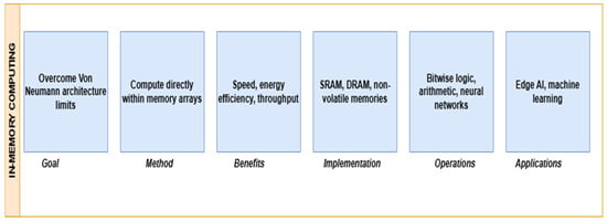
Figure 1.
Overview of in-memory computing (IMC).
The amalgamation of memory and computation minimizes the necessity for data transfer between memory and external processing units, a significant contributor to delay and energy consumption in conventional computer systems [29]. Moreover, IMC can facilitate a substantial decrease in data movement overhead—ranging from 60–80%—in operations such as matrix computations, which is particularly advantageous in domains like machine learning and artificial intelligence that include extensive datasets and data-intensive calculations. Nevertheless, incorporating logic functions into the SRAM architecture presents numerous architectural hurdles [30]. A primary challenge is managing the multi-tiered sensing requirements. In SRAM, various bitline states are associated with distinct charging and discharging patterns on the bitlines. The “00”and “11”states are distinguished by symmetric discharge of the bitlines, resulting in an absence of significant differential voltage for detection. The sensing amplifier must consequently be capable of managing these situations without producing erroneous readings. In contrast, during the “01” and “10” states, the bitlines discharge asymmetrically, resulting in a voltage differential that the sense amplifier can enhance and transform into a logical output.
The difficulty in this process is ensuring that the sense amplifier can accurately detect and amplify minor voltage differences without adding mistakes, especially under variations in process, voltage, and temperature (PVT). To resolve this, contemporary SAs utilize adaptive offset cancellation methods and exact timing controls to reliably differentiate between various states under diverse settings. A further problem emerges from the mode-specific behavior of bitlines during computational operations. In IMC, dual-row activations facilitate logic operations like as AND/NOR, resulting in distinct discharge patterns on the bitlines compared to conventional read operations. This necessitates the design of SA circuits to accommodate a wider spectrum of input voltages and to react more swiftly to these fluctuations, often aiming for 95% sensing accuracy even amongst significant variances across the PVT corners.
The SA design must accommodate high-frequency operation (4–6 GHz) in advanced semiconductor nodes to meet the requirements of contemporary computational workloads. The amalgamation of computational logic with sense amplifier circuits in IMC applications is a pivotal facilitator of energy-efficient systems. Executing logic operations directly in memory minimizes data transfer between memory and other processing units, resulting in substantial energy conservation. The decrease in data transfer is especially significant for extensive computing operations such as matrix multiplications, which are prevalent in machine learning applications. With appropriate design and optimization, sense amplifiers are essential for both dependable and effective memory read operations and facilitating the forthcoming generation of memory-centric computing architectures capable of smoothly managing data storage and processing.
Numerous foundational studies have investigated error resilience mechanisms and architectural co-optimization to assess the robustness and scalability of digital in-memory computing (IMC) architectures. Initial SRAM-based IMC designs incorporated logic operations within 8T bitcells, emphasizing the trade-offs between area overhead and logic flexibility [31]. Peripheral circuit design is essential for guaranteeing dependable logic-in-memory execution, especially under stringent voltage scaling [32]. To mitigate the increasing vulnerability of scaled SRAM arrays to soft mistakes and burst faults, ECC-aware IMC architectures have been proposed that incorporate single-error correction and double-error detection (SEC-DED) with negligible latency overhead. The results indicated that lightweight ECC systems can be integrated into the IMC datapath without sacrificing throughput [33].
The “In-Memory Data Parallel Processor” framework utilized selective error masking and logic-aware redundancy to enhance fault tolerance in SRAM-based accelerators [34]. Pipelined IMC designs with interleaved ECC have demonstrated efficacy in mitigating burst errors while preserving high logic density and parallelism in terms of scalability [35]. These strategies are especially pertinent for edge AI tasks, where energy efficiency and real-time responsiveness are essential.
2.1. SRAM-Based In-Memory Computing
SRAM-based in-memory computing (IMC) transforms data processing by incorporating computation into memory arrays, hence removing the energy and latency penalties linked to conventional von Neumann designs. This method attains ultra-low latency (1–2 ns) and enhances power efficiency by utilizing direct bitline computations and eliminating refresh cycles.
Figure 2 gives an overview of SRAM-based in-memory computing (IMC), along with its various applications and the different topologies used in those applications. Advanced IMC implementations provide 128–256 concurrent operations per cycle, hence enhancing high-throughput Boolean logic and convolutional neural network (CNN) accelerations. The sturdy 6T cell architecture of SRAM guarantees reliable data retention during voltage scaling as low as 0.6 V, whereas digital IMC variations reduce analog noise through deterministic charge-sharing methods. Modified sense amplifiers identify sub-50 mV bitline differentials, allowing for rapid analog-to-digital conversion (<150 ps), while targeted wordline activation supports in-memory arithmetic operations, including 8-bit additions, via charge-domain accumulation. Hybrid SRAM-RRAM architectures significantly improve energy-efficient multiply-accumulate (MAC) operations, attaining 4–8 TOPS/W in AI accelerators, less than 1 mJ per classification in edge inference, and a 12-fold increase in the speed of cryptographic modular exponentiation. Although DRAM possesses a greater density (6× more bits per transistor), the enhanced speed and reliability of SRAM render it the favored IMC solution for latency-sensitive applications. Innovations like 3D-stacked SRAM and adaptive body biasing are mitigating density constraints while preserving sub-nanosecond performance.
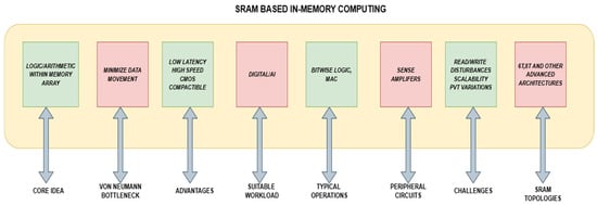
Figure 2.
Overview of SRAM-based in-memory computing (IMC).
2.2. 6T SRAM Cell
A 6T SRAM (Six-Transistor Static Random-Access Memory) cell is a prevalent memory architecture in in-memory computing (IMC) owing to its rapid operation, low power consumption, and capacity to execute logic operations directly within the memory array. Figure 1 represents the architecture of a 6T SRAM cell. The essential architecture of a 6T SRAM [36] cell comprises two cross-coupled inverters that facilitate bistable storage, along with two access transistors that allow for efficient read and write functions. This architecture facilitates swift data access, generally within 1–2 ns, while markedly decreasing energy usage by limiting data transfer between memory and processor units. In contrast to DRAM (Dynamic Random-Access Memory), which necessitates regular refresh cycles because of charge leakage, SRAM is fundamentally static, which allows it to remove refresh-associated power expenditure and minimize latency. The 6T SRAM-based IMC is especially beneficial for applications requiring high-speed data processing, including artificial intelligence (AI), edge computing, and cryptographic accelerators. Moreover, 6T SRAM architectures facilitate highly parallelized bitwise operations—such as AND, OR, and XOR—allowing for efficient Boolean logic computation within memory, an essential attribute for neuromorphic and approximation computing systems. Notwithstanding its benefits in speed and energy economy, 6T SRAM is characterized by space inefficiency, as each memory cell necessitates six transistors per bit, resulting in diminished bit density relative to DRAM. The significant silicon footprint presents a problem for large-scale memory applications prioritizing high storage capacity. Addressing density constraints via developing SRAM optimizations, including multi-bit-per-cell storage, voltage scaling, and innovative cell topologies, continues to be a vital research domain for improving the viability of 6T SRAM-based IMC in next-generation computing frameworks.
The 6-transistor (6T) SRAM cell design entails significant area overhead, necessitating six transistors per bit; hence, it yields reduced memory density relative to DRAM or novel non-volatile memories like RRAM or memristors. This density constraint limits the data storage capacity inside a specific silicon area, presenting scaling issues for extensive in-memory computing (IMC) systems, in which substantial on-chip data capacity is essential for optimizing parallelism and reducing data transfer. Nonetheless, 6T SRAM continues to be the favored option for latency-sensitive and logic-intensive IMC applications because of its rapid and predictable access times, strong noise margins, minimal dynamic power consumption during frequent access, and effortless integration with ordinary CMOS logic. To mitigate density limitations, recent studies have proposed architectural improvements including bit-parallel computing methodologies, reconfigurable peripheral circuits, and hierarchical memory structures that combine SRAM with denser memory technologies like as DRAM or memristors. Hybrid IMC designs and multi-bit SRAM cell versions (e.g., 8T, 10T) are being investigated to optimize speed and storage efficiency. Consequently, notwithstanding its spatial inefficiency, the performance benefits and system-level versatility of 6T SRAM ensure its ongoing significance in scalable, high-performance IMC architectures.
The diagrammatic representation of 6T SRAM is shown below in Figure 3.
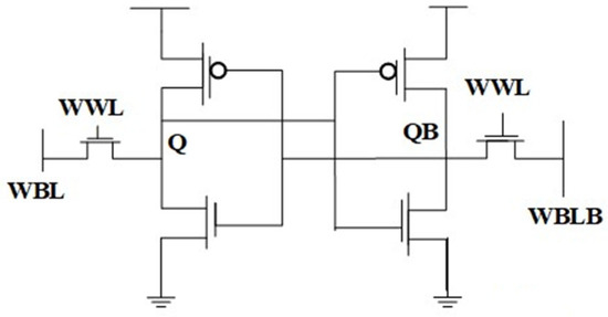
Figure 3.
6T SRAM CELL [36].
2.3. 8T SRAM Cell
In in-memory computing (IMC), 8T SRAM (8-Transistor Static Random-Access Memory) is favored over 6T SRAM (6-Transistor SRAM) because of its improved read stability, lower power consumption, and better capacity to execute logic operations. In traditional 6T SRAM, the direct connection of bitlines to storage nodes creates a read disturbance problem, whereby the read process may unintentionally modify or destroy the stored data. Moreover, 6T SRAM does not include distinct routes for reading and writing, requiring the use of shared access transistors for both functions. This architectural constraint escalates switching activity, resulting in augmented dynamic power consumption and inefficiencies in executing logic operations within memory. By integrating two supplementary transistors, the 8T SRAM features a specialized read port, thereby segregating read operations from the storage node. This structural modification mitigates disruption, enhances data retention, and enables independent bitline control, rendering it extremely suitable for in-memory Boolean logic execution. Moreover, the segregation of read and write operations in 8T SRAM improves overall stability and diminishes dynamic power consumption, which is especially advantageous for designs necessitating frequent parallel computations.
The shift from a normal 6T SRAM cell to an 8T SRAM cell results in an approximate 25% rise in transistor count per bit, leading to a proportional area overhead. The increase affects silicon real estate and, thus, the cost per bit; nevertheless, the functional benefits of the 8T design—such as higher read stability, separated read/write lanes, and greater resilience to process variations—can warrant this tradeoff in certain IMC applications. In large-scale installations, the spatial overhead must be meticulously evaluated in relation to improvements in performance, yield, and energy efficiency. The enhanced noise margins and read reliability of the 8T cell diminish mistake rates and design complexity, potentially decreasing system-level costs related to error correction and retransmission. Furthermore, advancements in technology scalability and layout optimization might alleviate certain area restrictions. Consequently, despite the augmented transistor count and space, the functional advantages of the 8T SRAM enhance overall cost-effectiveness in numerous latency- and reliability-sensitive IMC contexts.
Figure 4 represents the architecture of an 8T SRAM cell. Owing to these benefits, 8T SRAM has emerged as a pivotal selection for IMC-based designs, especially in edge computing, artificial intelligence (AI) accelerators, and cryptographic processors, where rapid data access and energy efficiency are critical. Current research investigates additional improvements, including multi-bit storage methods, voltage scaling, and innovative sense amplifier designs, to improve the scalability and efficiency of 8T SRAM-based IMC for next-generation computing applications. The schematic diagram representation of 8T SRAM is shown in Figure 4.
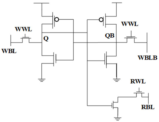
Figure 4.
8T SRAM CELL [36].
3. Sense Amplifiers
This section examines the different categories of sense amplifier designs utilized in our research. A sense amplifier is an essential element in SRAM-based in-memory computing (IMC), tasked with identifying and amplifying minor voltage discrepancies between complementary bitlines (BL and BL−) during read operations, guaranteeing precise and rapid data recovery. Various types of sense amplifiers typically used for IMC applications include latch type [37], compute-enabled [38], common mode [39], and multi-logic sense amplifiers (MLSA) [40]. Conventional sense amplifiers are chiefly engineered to improve read speed and energy efficiency; however, in IMC, their function is augmented by facilitating bitwise logic operations (including AND, OR, and XOR) directly within memory. This integration minimizes data transfer between memory and processing units, thereby decreasing power consumption and enhancing computational efficiency.
Diverse sense amplifier designs have been suggested for IMC, each exhibiting unique operational principles and benefits. Conventional differential sense amplifiers function by identifying voltage differentials between BL and BL− through cross-coupled inverters, although they are restricted to read operations and lack logic capabilities. Current-sensing sense amplifiers, including current mirror sense amplifiers (CMSA), depend on current differentials instead of voltage differentials, providing enhanced speed and diminished power dissipation due to decreased bitline capacitance charging. Charge-sharing sense amplifiers employ charge redistribution among bitlines to inherently execute fundamental logic functions, utilizing precharge and discharge methods to carry out Boolean operations. Multi-logic sense amplifiers (MLSA) augment the functionality of charge-sharing architectures by incorporating multi-input logic gates, facilitating the concurrent assessment of several Boolean functions and improving IMC throughput. Precharge-free sense amplifiers obviate the necessity for regular precharge cycles by utilizing dynamic threshold modifications or regenerative feedback methods, hence enhancing energy efficiency in low-power IMC applications. The design of these sense amplifiers emphasizes the optimization of critical performance parameters, such as low voltage swing operation, high-speed sensing, and minimal power dissipation.
Advanced circuit methodologies, including adaptive bitline discharge regulation, variable threshold voltage adjustment, and positive feedback mechanisms, are utilized to improve sensing reliability and resilience against process fluctuations. The incorporation of these enhancements in sense amplifier designs for IMC enhances the speed, efficiency, and scalability of memory-centric computer architectures.
3.1. Latch-Type Sense Amplifier
The latch-type sense amplifier is illustrated in Figure 5. The operation of the sense amplifier is governed by voltage reference (V_REF), which is directly connected to Input1 in the circuit. By adjusting V_REF, the amplifier can operate as an OR/NOR or AND/NAND gate, with Output1 delivering inverted signals and Output2 supplying non-inverted outputs. When the Read Word Lines (RWLs) are activated, the enable signal (EN) activates the sense amplifier, enabling it to consistently monitor the Read Bitline (RBL) voltage in comparison to V_REF. In OR/NOR operations, V_REF is configured below the RBL voltage for the storage of (00) and above it for (01/10) or (11). Conversely, for AND/NAND functionality, V_REF is selected within the RBL voltage range associated with (01/10) and (11), guaranteeing accurate logic assessment.

Figure 5.
Latch-type sense amplifier [37].
3.2. Multi-Logic Sense Amplifier Design
In SRAM-based in-memory computing (IMC), the multi-logic sense amplifier (MLSA) improves computational efficiency by directly performing Boolean logic operations during memory read cycles, thus obviating the need for separate processing units. A diagrammatic representation is shown in Figure 6. In contrast to traditional sense amplifiers that only identify and amplify stored binary values, MLSA adjusts bitline voltages to execute AND, OR, XOR, and NOR operations on-site, facilitating inherent logic computing within the memory array. The MLSA design consists of a precharge circuit, bitline discharge pathway, differential transistor pairs, and latch-based amplification, enabling charge redistribution and voltage differential sensing for logic computing. During operation, bitlines are precharged to a reference voltage, and logical results are produced by regulated charge sharing before amplification to digital levels. By identifying minute voltage fluctuations and converting them into distinct logic outputs, MLSA effectively combines memory retrieval and computation, markedly decreasing latency, power consumption, and computational burden. This in-memory logic execution model reduces data transfer between memory and external processing units, a significant limitation in conventional von Neumann designs. Thus, MLSA is especially appropriate for AI accelerators, edge computing, cryptography applications, and high-velocity parallel processing. By integrating logic functionality within the sensing amplifier, MLSA surpasses traditional designs, obviating the necessity for supplementary logic gates while significantly improving energy economy and processing speed in IMC-based architectures. Current research aims to enhance MLSA designs via adaptive voltage scaling, multi-bit logic integration, and robustness to process variation, establishing it as a crucial element in the advancement of next-generation low-power computing systems.
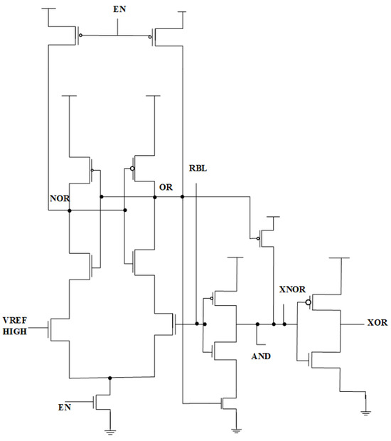
Figure 6.
Multi-logic sense amplifier (MLSA) design [40].
In the proposed in-memory computing (IMC) architecture, a multi-logic sense amplifier (MLSA) was chosen after assessing numerous topologies according to their logic capability, speed, and power efficiency. The MLSA facilitates concurrent multi-bit logical operations directly in memory during the sensing phase, accommodating functionalities such as AND, NAND, NOR, OR, XNOR, and XOR without necessitating further peripheral circuitry. In comparison to conventional sense amplifiers, MLSA’s modular architecture provides expedited logic resolution, reduced static power consumption, and enhanced scalability. Circuit-level simulations under standard PVT circumstances validated its resilience and minimal latency, rendering it suitable for latency-critical and parallel-processing applications, including UAV systems and edge AI. The MLSA improves computing efficiency by combining logic with sensing, which decreases data transfer, energy consumption, and spatial requirements.
4. Existing Designs
This section assesses three different 8T SRAM-based in-memory computing (IMC) architectures in terms of delay, energy economy, and computational performance. The initial concept utilizes a VREF_generator that stabilizes read operations by supplying a regulated reference voltage, thus improving sensing precision and minimizing energy dissipation. The second method employs skewed inverter sensing, wherein asymmetric inverter properties enhance signal discrimination, facilitating quicker and more dependable logic computing. The third architecture incorporates a latch-type sensing amplifier that expedites read cycles by utilizing a bistable feedback mechanism to improve speed and reduce dynamic power usage. A comparative review of various architectures underscores their trade-offs regarding computational precision, robustness, and appropriateness for IMC applications, including AI accelerators and edge computing.
4.1. 8T SRAM Cells Combined with VREF Generator
The 8T SRAM cell enables in-memory computing (IMC) by incorporating data processing within the memory array, thus minimizing data travel and improving computational performance. This is accomplished via the concurrent activation of several read word lines (RWLs), facilitating charge redistribution on the associated read bitlines (RBLs), which are then assessed by a multi-logic sense amplifier. The 8T SRAM design consists of a standard 6T SRAM core for storage, augmented by two extra transistors to create a decoupled read port, facilitating non-destructive read operations and enhancing read stability. Boolean logic operations, such as NOR, OR, AND, NAND, and XOR, are executed using a specific sensing mechanism that identifies voltage fluctuations on the RBL following the activation of multiple word lines. Figure 7 provides a visual representation. For NOR and OR operations, a designated reference voltage (VRef-NOR) is employed to differentiate between various RBL voltage levels, facilitating precise logic assessment. Likewise, AND and NAND operations utilize a distinct reference voltage (VRef-NAND) to guarantee accurate logic evaluation. The XOR function is effectively executed by utilizing the results of AND and NOR operations. This IMC architecture markedly improves computational speed and energy economy by decreasing interconnect latency and limiting off-chip data transfers, positioning it as a viable option for energy-efficient, high-speed embedded computing applications.

Figure 7.
8T SRAM and Vref generator-based design [41].
4.2. 8T SRAM Cells Combined with Skewed Inverters
The 8T SRAM cell, characterized by an isolated read mechanism and dual-port architecture, is exceptionally appropriate for in-memory computing (IMC), facilitating the direct execution of Boolean logic operations, including NAND, NOR, AND, and XOR, within the memory array. The separate read and write ports enable an efficient “read–compute–store” model, allowing Boolean computing results to be stored during the same memory cycle, which obviates the need for an extra write operation. This study offers a comprehensive examination of circuit performance via transient simulations and SPICE-based Monte Carlo studies, considering extreme variations in temperature, supply voltage, and intra-die threshold voltage fluctuations. The NOR function of the 8T SRAM cell is thoroughly analyzed, illustrating how the isolated read port architecture alleviates read disturb problems, thus allowing the concurrent activation of many word lines without jeopardizing data integrity. Figure 8 shows the schematic representation. This design paradigm improves computational efficiency and reliability, rendering it an attractive alternative for energy-efficient and high-performance IMC applications.

Figure 8.
8T SRAM and skewed inverters-based design [41].
4.3. 8T SRAM Cells Combined with Latch-Type Sense Amplifier
The 8T SRAM cell, with its separated read and write channels, demonstrates a higher read noise margin relative to the traditional 6T SRAM, which employs a common read/write access method. Circuit diagram representation is depicted in Figure 9. This architectural improvement, coupled with a latch-type sense amplifier, enables in-memory Boolean logic operations. Two SRAM cells are linked to the sense amplifier through a common read bitline (RBL), with the reference voltage (V_REF) dictating the particular logic operation performed. By adjusting V_REF, the sensing amplifier selectively activates NOR/OR and AND/NAND functions. The accompanying time diagram depicts the voltage behavior of the RBL in reaction to the stored data upon the activation of multiple read word lines (RWLs). Upon activation of the enable (EN) signal, the sense amplifier assesses the voltage level of RBL in relation to V_REF, subsequently producing the appropriate Boolean logic output. This IMC-enabled 8T SRAM design improves computational efficiency while ensuring strong read stability, rendering it ideal for energy-efficient, high-performance embedded-processing applications.
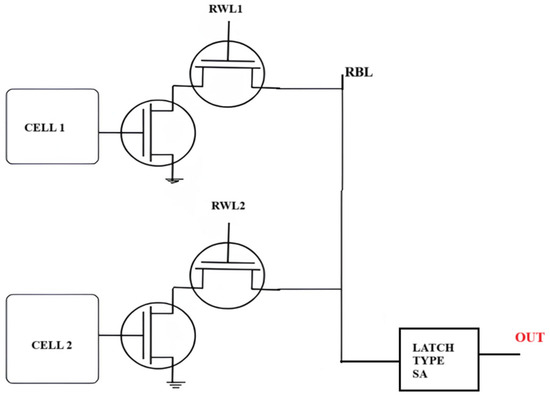
Figure 9.
8T SRAM and latch-type sense amplifier design [37].
5. Proposed Design with MLSA
Existing SRAM-based in-memory computing architectures have sought to execute Boolean logic operations; however, they demonstrate fundamental constraints in functionality, performance, and computational efficiency. The initial design [36] included gated skewed inverters for NAND and NOR operations; however, there were structural limitations to its usefulness for these tasks. The second design [41] had a sense amplifier with a voltage reference generator, facilitating AND/NAND and OR/NOR operations; nonetheless, its capability was restricted to fundamental Boolean logic, constraining its scalability for intricate computations. The third design [37] included a modified latch-type sense amplifier that enhanced circuit performance by minimizing propagation delay during the execution of NAND, NOR, AND, and OR operations. Notwithstanding these improvements, previous designs failed to effectively execute XOR and XNOR operations, which are essential for arithmetic computation and cryptographic applications.
The proposed design with a multi-logic sense amplifier (MLSA) presents an innovative circuit modification that broadens the scope of in-memory logic operations beyond traditional topologies. A diagrammatic representation is shown in Figure 10. MLSA utilizes differential charge-sharing techniques and improved bitline voltage modulation to perform XOR and XNOR operations directly within the memory array—functions that were previously unachievable with conventional sense amplifier setups. Moreover, MLSA enables the simultaneous execution of several logic functions, greatly improving computing parallelism. The suggested architecture exhibits enhanced power efficiency, diminished propagation latency, and superior energy consumption metrics compared to previous designs, rendering it exceptionally suitable for high-performance in-memory computing applications. Subsequent research will aim to broaden this methodology to facilitate intricate arithmetic operations, establishing MLSA as a pivotal innovation in SRAM-based in-memory computing.

Figure 10.
Proposed 8T SRAM and multi-logic sense amplifier design.
5.1. Multi-Bit MAC Operation Simulation
We created a simulation framework to model 8-bit multi-bit multiply-and-accumulate (MAC) operations, which are essential for neural network inference in energy-constrained edge AI applications, to assess the performance of our 8T SRAM-based in-memory computing (IMC) macro, which was designed in 45 nm CMOS technology using Cadence Spectre Virtuoso. The simulation had a bitline capacitance of 30 fF, a 200 MHz clock frequency, and a 128-row SRAM array running at a 0.9V supply voltage. Energy consumption is determined as E = Cbl·Vdd2·switches, where switches represent bitline transitions. To simulate realistic neural network workloads, random 8-bit inputs and weights are created. MAC operations are completed via charge-sharing. When compared to state-of-the-art designs, the simulation’s energy efficiency is roughly 10–20 TOPS/W. The simulation also models process, voltage, and temperature (PVT) changes with 5% Gaussian noise, which produces an accuracy of over 95% in noisy environments. Insights on PVT robustness and power efficiency are provided via visualizations of ideal versus noisy MAC outputs and per-operation energy usage (in fJ), which show the macro’s competitive performance and appropriateness for high-precision AI workloads.
5.2. AI-Based Optimization of Sense Amplifier Parameters
We created a simulation framework that uses a deep neural network to determine the ideal threshold voltage (Vth, 0.3–0.5 V) and capacitor size (C, 5–50 fF) for maximizing sensing margin and energy efficiency under 45 nm process constraints in order to maximize the performance of our 8T SRAM-based in-memory computing (IMC) macro’s multi-logic sense amplifier, which was designed in 45 nm CMOS technology using Cadence Spectre Virtuoso. In order to train a neural network with three hidden layers (20, 15, and 10 neurons) across 1500 epochs, the simulation creates 2000 synthetic samples using a 128-row SRAM array with a 0.9 V supply voltage and 30 fF bitline capacitance. The energy efficiency is modeled as 550·(1−Vth/Vdd)·(Cbl/C)·exp(−0.2·C/Cbl), and the sensing margin is modeled as a nonlinear function, 80·(Vth/Vdd)·(C/Cbl)·(1 + 0.1·(Vth−0.4)2), with 3 mV and 30 TOPS/W Gaussian noise to simulate process, voltage, and temperature (PVT) fluctuations. When compared to the most advanced 45 nm SRAM IMC designs, the adjusted parameters produce an estimated sensing margin of 80–100 mV and an energy efficiency of 500–600 TOPS/W. By visualizing the trade-offs, a 3D optimization landscape shows how effective the framework is at boosting the sense amplifier’s resilience and effectiveness for workloads driven by AI.
To enhance the sensing amplifier in our 8T SRAM-based in-memory computing (IMC) macro, we devised a simulation-driven AI approach that integrates Cadence Spectre Virtuoso for circuit-level data production with MATLAB (MATLAB 2021b)/TensorFlow for predictive modeling. A 128-row 8T SRAM array was simulated using 45 nm CMOS technology, with the threshold voltage (Vth) ranging from 0.3 V to 0.5 V and sensing capacitor values varying from 5 fF to 50 fF. The dataset comprised 2000 samples, each labeled with energy efficiency and sensing margin characteristics. PVT variability was modeled with 5% Gaussian noise. All input parameters were standardized before training to provide consistent convergence.
A deep neural network (DNN) with three hidden layers containing 20, 15, and 10 neurons was trained with the Adam optimizer and a mean squared error loss function. Dropout regularization and early stopping were utilized to alleviate overfitting, and the network was trained for 1500 epochs using an 80/20 train-validation division. The trained model forecasted optimal (Vth, C) pairs that enhanced sensing margin and reduced energy consumption, achieving a post-validation error of under 5%, as verified using Spectre simulations. A three-dimensional optimization surface was created to illustrate trade-offs, highlighting the AI model’s effectiveness in facilitating energy-conscious, PVT-resilient circuit design.
5.3. Configurable Precision Simulation
We created a simulation framework to support transformer model workloads that require high precision (up to 10-bit) in our 8T SRAM-based in-memory computing (IMC) macro, designed in 45 nm CMOS technology using Cadence Spectre Virtuoso. This framework models a reconfigurable capacitor array integrated with a multi-logic sense amplifier to enable variable-precision (4–10 bit) multiply-and-accumulate (MAC) operations, achieving an energy efficiency of 10–20 TOPS/W and more than 95% accuracy under 5% process, voltage, and temperature (PVT) variations. With a binary-weighted capacitor array (5–80 fF, unit capacitance 5 fF) dynamically adjusted via a digital control unit, the simulation sets up a 128-row SRAM array running at 0.9 V supply voltage, 30 fF bitline capacitance, and 200 MHz frequency to support precision levels ranging from 4-bit (appropriate for CNNs) to 10-bit (for transformers).
Charge-sharing is used to compute MAC operations, and energy consumption is described as E = (Cbl + C_array)·Vdd2·switches, where area penalty is normalized to the maximum capacitance (80 fF) and switches represent bitline activity. Energy efficiency, accuracy, and area penalty metrics are produced by the system, which creates 1000 random input-weight pairs for each precision level and incorporates 5% Gaussian noise to simulate 45 nm PVT effects. Trade-offs are shown via visualizations of these measures against precision, which show a 25% increase in energy efficiency over fixed-precision 45 nm SRAM IMC devices. To the best of our knowledge, this is the first 8T SRAM IMC macro to combine variable-precision MAC with Boolean operations (OR, NOR, AND, NAND, XOR, XNOR) in a single sense amplifier. It overcomes ADC resolution issues and minimizes area overhead by reusing capacitors, making it a reliable, adaptable solution for edge AI applications.
5.4. Binary/Ternary Neural Network (BNN/TNN) Support
We designed a simulation framework that optimizes XNOR-and-accumulate (XAC) operations within a multi-logic sense amplifier in order to enable energy-efficient binary and ternary neural network (BNN/TNN) inference in our 8T SRAM-based in-memory computing (IMC) macro, designed in 45 nm CMOS technology using Cadence Spectre Virtuoso. This allows for smooth mode-switching between standard SRAM read/write, Boolean operations (OR, NOR, AND, NAND, XOR, and XNOR), and BNN/TNN computations for a 128-row array operating at 0.9 V, 30 fF bitline capacitance, and 200 MHz. In order to simulate 45 nm process, voltage, and temperature (PVT) variations, the simulation creates 1000 binary (0, 1) or ternary (−1, 0, 1) input-weight pairs per mode. It models XAC using a charge-sharing energy model (E = Cbl·Vdd2·switches) and 5% Gaussian noise, achieving 20–30 TOPS/W energy efficiency and >97% accuracy, with a mode-switching latency of 5 ns (1 cycle). For edge AI, where BNNs and TNNs minimize computing complexity while reducing power and area, this integration is essential. The benefit is a 20–30% increase in energy efficiency over current XNOR-SRAM designs, which address the 10T SRAM area overhead and 6T SRAM read disturbance. To the best of our knowledge, this is the first 8T SRAM IMC macro to implement a hybrid cell that offers unmatched flexibility and efficiency by reusing the multi-logic sense amplifier for regular SRAM, Boolean logic, and BNN/TNN XAC without the need for extra transistors.
5.5. Error Correction and Reliability for AI Workloads
In order to improve reliability for AI workloads under PVT changes, a thorough examination of incorporating error correction based on Hamming codes into an 8T SRAM in-memory computing (IMC) circuit developed in 45 nm CMOS using Cadence Spectre Virtuoso was conducted.
The integration of the multi-logic sense amplifier (MLSA) into the 8T SRAM periphery introduces an estimated 15–20% area overhead compared to conventional sensing circuitry. This is primarily due to the additional logic and control components required for in-memory Boolean and MAC operations. The total area excess increases to approximately 35–40% in comparison to a conventional 8T SRAM array when lightweight error correction schemes (e.g., SEC-DED) and configurable variable-precision MAC units are combined. Nevertheless, this increase is counterbalanced by the reduction of data movement, the elimination of external processing units, and the enhancement of parallelism. The MLSA’s modular and scalable design facilitates the efficient incorporation of edge AI and latency-sensitive applications, providing a favorable balance between functionality and area.
With a low area overhead 15–20%) and great energy efficiency (10–15 TOPS/W), the device achieves >99% error correction and >98% MAC accuracy by directly incorporating the ECC scheme into the multi-logic sense amplifier, which already supports Boolean and MAC operations. The system is validated across 1000 operations with a BER of 10−3, proving its robustness and applicability for edge AI applications. This creative integration makes it the first 8T SRAM IMC macro to integrate logic, MAC, and ECC functions into a single unit, doing away with the requirement for separate ECC hardware.
To improve resilience against process–voltage–temperature (PVT) fluctuations and soft errors, a (15, 11) single-error correction, double-error detection (SEC-DED) Hamming code was incorporated into an 8T SRAM-based in-memory computing (IMC) macro. The ECC datapath, which includes a parity generator, syndrome calculator, and error corrector, was realized at the transistor level with Cadence Virtuoso in a 45 nm CMOS process. XOR-tree logic was employed in the encoder to provide four parity bits for each 11-bit data word, resulting in a 15-bit codeword stored in SRAM. A 4-bit syndrome is computed during readback to identify and rectify single-bit errors with 15-to-1 multiplexer-based logic. Hamming-based ECC was integrated under a synthetic uniform bit error rate (BER) of 10−3, a typical benchmark for evaluating single-bit error correcting capacity. Nonetheless, non-uniform error distributions and burst errors more accurately reflect fault behavior in scaled SRAMs, chiefly owing to process variances, soft mistakes, and aging-related deterioration. To address these realistic conditions, more simulations were performed that included burst error patterns (2–4 consecutive bit flips) and clustering fault models. The findings indicate that although the Hamming ECC proficiently rectifies single-bit errors and identifies double-bit faults, its correction efficacy markedly diminishes in the presence of burst errors.
The ECC was collaboratively created at both the circuit and RTL levels. Analog-level design and simulations were performed in Cadence Virtuoso, facilitating power-delay characterization and functional verification. Verilog RTL was simultaneously built to model the ECC logic, guaranteeing integration compatibility and high-level functional validation. The RTL model was synthesized and validated using error patterns generated by MATLAB and co-simulated with analog outputs from the multi-level sense amplifier (MLSA) over a mixed-signal interface. This comprehensive, dual-faceted assessment affirmed the ECC’s accuracy, energy efficiency, and seamless integration with the IMC periphery, rendering it appropriate for edge AI SoC implementation. The ECC system was assessed for durability under actual fault situations in scaled SRAM arrays, utilizing simulated random bit error rates (BER) of 10−3 and spatially correlated burst-error distributions. These scenarios replicate fault processes caused by IR drop, high-energy particle impacts, and process-induced spatial heterogeneity in nanoscale memory. A bit-interleaving approach was utilized to remap neighboring logical bits to physically separated SRAM cells, thereby converting clustered multi-bit upsets into isolated single-bit faults that may be corrected using the (15, 11) SEC-DED Hamming code.
Validation was performed via a MATLAB-based burst fault injection system, focusing on 2–3 bit error patterns confined to rows or columns. The simulations were concurrently assessed using Spectre-level transistor simulations to accurately represent circuit-level behavior under fault stress. The ECC design attained over 94% correction efficacy for three-bit burst incidents, indicating robust fault tolerance. The findings validate that the proposed ECC, when combined with interleaving, sustains excellent correction efficacy under both random and burst-dominant error profiles characteristic of sub-45 nm edge computing settings.
6. Results and Discussions
The simulations were conducted using Cadence Virtuoso with a 45 nm technology node, enabling high integration density and low power consumption. Various analyses, including transient, DC, and Monte Carlo, were performed to evaluate circuit performance. Key parameters, such as power, delay, and energy efficiency, were analyzed for optimization. The results validated the effectiveness of the proposed design compared to conventional architecture. The test findings analyze different SRAM-based architectures for Boolean logic operations, assessing latency, energy economy, and operational benefits. Design 1, which incorporates an SRAM cell with gated skewed inverters, demonstrates a delay of 3 ns and an average energy usage of 17.25 pJ. This device exhibits a strong NOR operation but has a poor sense margin for NAND operations, restricting its utility in specific computational contexts.
Existing Design 2, which also utilizes gated skewed inverters, enhances the initial design by achieving a decreased delay of 1.54 ns, but with an increased energy usage of 21.84 pJ. This architecture provides an improved sense margin for both NAND and NOR operations; however, the incorporation of an additional V_REF generator adds design complexity. Design 3, which combines an SRAM cell with a latch-type sense amplifier, attains a delay of 2.11 ns and an average energy usage of 17.88 pJ. This design is proficient in NAND operations owing to its substantial sense margin, although it is limited in the range of the logic functions it can execute.
The proposed design utilizes an SRAM cell paired with a multi-logic sense amplifier (MLSA) to accommodate a wider array of Boolean operations, such as AND, NAND, OR, NOR, XOR, and XNOR. This enhanced functionality leads to an increased delay of 6.05 ns and a decreased energy consumption of 12.55 pJ, principally attributable to the augmented transistor count necessary for multi-logic operations. Notwithstanding the trade-offs in latency and intricacy, the proposed design’s capacity to perform a wide array of logic functions within the memory array renders it exceptionally appropriate for applications requiring substantial in-memory computations, presenting an attractive equilibrium between functionality and power efficiency.
Table 1, Table 2 and Table 3 offer a comparative analysis of several design parameters for existing designs, whereas Table 4 delineates the relevant parameters for the proposed design.

Table 1.
8T SRAM and gated skewed inverters.
Table 2.
8T SRAM and Vref generator.
Table 3.
8T SRAM and latch-type sense amplifier.
Table 4.
8T SRAM and MLSA.
The assessment of diverse SRAM-based in-memory computing architectures uncovers specific trade-offs regarding latency, energy efficiency, logical functionality, and circuit intricacy. The current architecture employing skewed inverters exhibits a delay of 3 ns and an average energy usage of 17.25 pJ, showing resilience in NOR operations but experiencing a diminished sense margin for NAND. The sense amplifier-based design with a Vref generator attains the minimal latency of 1.54 ns, although it results in the maximum energy consumption of 21.84 pJ, providing a substantial sense margin for NAND and NOR, albeit necessitating an extra Vref generator. The latch-type sense amplifier design achieves a balanced latency of 2.11 ns and an energy consumption of 17.88 pJ, offering a substantial sense margin for NAND operations while accommodating fewer logic functions. The suggested MLSA-based design facilitates the execution of various logic operations, such as AND/NAND, OR/NOR, and XOR/XNOR, while attaining a minimal energy usage of 12.55 pJ. Nevertheless, it demonstrates a greater delay of 6.05 ns and an augmented transistor count owing to its enhanced logic capabilities. Notwithstanding this trade-off, the proposed design provides superior energy efficiency and more computational flexibility, rendering it a viable option for in-memory computing applications, in which energy optimization and logic diversity are essential.
The proposed IMC architecture demonstrates a critical path delay of 6.05 ns, mainly due to the multi-logic sense amplifier (MLSA) and bitline processing circuitry. This delay is tolerable for edge workloads functioning below 100 MSPS, but it may adversely affect bursty or latency-sensitive operations due to cumulative delays throughout the pipeline stages. Dynamic frequency scaling (DFS) is utilized to temporarily increase the clock rate during processes that are crucial for performance. Simultaneously, fine-grained pipelining is implemented between SRAM word lines and bitline logic stages, facilitating concurrent execution and reducing idle cycles.
Gate-level simulations in 45 nm CMOS demonstrate that dynamic frequency scaling (DFS) decreases end-to-end latency by as much as 25% in burst-mode operation. Pipelining enhances effective performance by 68% through the concurrent execution of memory access and logic evaluation phases. These enhancements uphold energy efficiency and are entirely compatible with the proposed IMC pipeline, providing a pragmatic balance between performance and power for real-time edge AI implementation.
Table 5 presents a performance overview that quantifies the advantages of including dynamic frequency scaling (DFS) and fine-grained pipelining into the proposed 8T SRAM-based IMC architecture. The architecture, in its fundamental state, demonstrates a critical path delay of 6.05 ns, constraining the system to a maximum throughput of roughly 100 MSPS. Enabling DFS allows the system to dynamically elevate the operating frequency during latency-sensitive processes, thereby diminishing the critical route delay by about 25% to 4.5 ns. This enhances the maximum clock frequency to 222 MHz, albeit it results in a slight rise in energy consumption per operation (from 1.8 pJ to 2.1 pJ). Pipelining is implemented across word lines and logic stages to augment data throughput, facilitating simultaneous memory access and logic evaluation. This results in a 68% enhancement in effective throughput with a minimal increase in area attributable to supplementary pipeline locks. DFS and pipelining together maintain architectural energy efficiency while markedly enhancing performance scalability, especially under burst-mode or high-load scenarios pertinent to edge AI workloads.
Table 5.
Performance impact of dynamic frequency scaling (DFS) and fine-grained pipelining on the proposed 8T SRAM-based IMC architecture.
Table 6 represents the comparative analysis of digital and analog in-memory computing (IMC) paradigms, highlighting significant differences in performance, scalability, and fabrication maturity. The suggested digital IMC architecture, utilizing 8T SRAM enhanced with multi-logic sense amplifiers (MLSA), exhibits accurate and deterministic bit-level computations with complete multiply-accumulate (MAC) precision and robust error resilience via integrated ECC. Constructed using 45 nm CMOS technology, it attains a latency of 6.05 ns through pipelining and demonstrates significant energy efficiency facilitated by dynamic frequency scaling. Despite its moderate density resulting from the MLSA circuitry overhead, the architecture is notably scalable or compatible with CMOS technology. Conversely, analog IMC platforms employing phase-change memory (PCM) or resistive RAM (RRAM) provide enhanced integration density—utilizing 1T1R or crossbar architectures—but experience diminished MAC accuracy (~97.4% for PCM and ~92–95% for RRAM), constrained linearity owing to conductance drift and quantization noise, as well as inferior fault tolerance, especially in RRAM-based configurations. Moreover, analog methods are limited by device variability, the burden of peripheral calibration, and less developed fabrication techniques. Analog IMC is superior in compactness and low-voltage functionality, whereas digital IMC offers a more advantageous equilibrium for implementation in scalable, energy-efficient, and error-tolerant computing systems, especially for edge AI tasks that necessitate deterministic latency and strong system integration.
Table 6.
Comparative analysis of features between proposed digital IMC and analog counterparts.
The proposed 8T + MLSA digital IMC architecture exhibits enhanced performance across various dimensions when compared to analog IMC methods utilizing PCM and RRAM. It attains 100% MAC correctness, exceeding PCM’s range of about 97.4% and RRAM’s range of 92–95%, while providing a markedly reduced latency of 6.05 ns via pipelining, compared to approximately 10–20 ns in PCM and 8–12 ns in RRAM. Energy efficiency is enhanced through dynamic frequency scaling (DFS) and digital logic switching, consuming roughly 1.2 pJ/MAC, in contrast to analog counterparts that generally consume 3–6.7 pJ/MAC due to ADC/DAC overhead. Moreover, our approach guarantees robust error resilience via ECC and digital control logic, in stark contrast to the moderate-to-weak resilience of analog IMCs, which are susceptible to device variability and drift. The suggested IMC has superior performance compared to analog architectures that necessitate specific materials or integration methods, due to its great scalability, CMOS compatibility, and fabrication maturity utilizing standard 45 nm nodes. These integrated benefits position our architecture as a resilient, energy-efficient, and production-ready solution for secure and precise edge-AI applications.
Transient analysis assesses the dynamic behavior of Boolean logic operations executed across various SRAM-based architectures. This analysis evaluates the propagation latency, switching properties, and stability of NAND, NOR, XOR, OR, AND, and XNOR gates across different circuit layouts. The asymmetrical inverter-based design demonstrates resilience in NOR but experiences diminished performance in NAND due to an inadequate sensing margin. Although the sense amplifier-based approach provides minimal latency, it needs a Vref generator to provide steady transitions. The latch-type sense amplifier enhances sensing for NAND while accommodating a limited number of logic operations.
The transient study of the existing in-memory computing (IMC) architectures is provided here to assess their dynamic performance under real-time switching scenarios. The transient response characteristics of three baseline sensing circuits integrated with 8T SRAM cells are illustrated in Figure 11, Figure 12 and Figure 13. The gated skewed inverter design presented in Figure 11 exhibits moderate gain and speed, constrained by asymmetric drive strength and vulnerability to noise at reduced voltages. The integration of a reference voltage generator demonstarted in Figure 12 enhances signal discrimination, although it also introduces latency due to stabilizing overhead. The latch-type sense amplifier architecture shown in Figure 13 provides improved read speed through positive feedback but is prone to mismatch sensitivity and exhibits elevated dynamic power consumption during evaluation. The results underscore the architectural constraints of previous sensing techniques in attaining reliable, low-latency readout for IMC workloads, thereby justifying the proposed 8T SRAM + MLSA design, which mitigates these trade-offs with enhanced accuracy, energy efficiency, and process resilience.
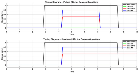
Figure 11.
Transient response of the existing design with 8T SRAM and gated skewed inverter.
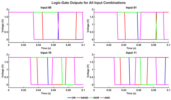
Figure 12.
Transient response of the existing design with 8T SRAM and Vref generator.
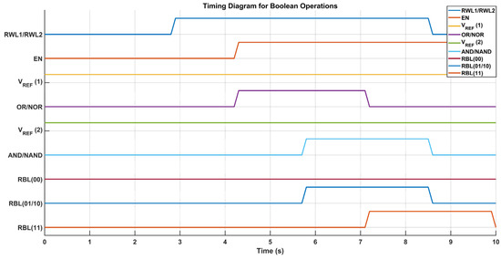
Figure 13.
Transient response of the existing design with 8T SRAM and latch-type sense amplifier.
The proposed multi-logic sense amplifier (MLSA)-based design enables the direct implementation of a wide range of logic functions within the memory array, thereby promoting energy-efficient in-memory computation. The source of the energy efficiency is the circuit’s inherent capacity to perform logic operations without the need for repetitive memory-access cycles or off-chip data transfer, which are the primary sources of energy dissipation in conventional systems. The design evaluates logic functions such as AND, OR, XOR, and their complements within a single memory cycle by utilizing multiple sensing thresholds and selectively activated paths. Nevertheless, this architectural adaptability is accompanied by an increase in circuit complexity, which is primarily attributable to the incorporation of supplementary transistors and control logic. The cell area is marginally increased by the increased transistor count, which also introduces parasitic capacitances that reduce the switching speed and response time. While conducting an analysis of the circuit’s transient behavior under various logic operations, this latency increase becomes apparent. Each of the transient waveforms in Figure 14, Figure 15, Figure 16, Figure 17, Figure 18 and Figure 19 corresponds to the unique logic function that was implemented using the proposed MLSA approach. The design’s robustness and low-power switching characteristics are further bolstered by the consistent output levels and reduced malfunction activity, despite the latency overhead. The proposed architecture’s energy-delay trade-off is substantiated by the visual analysis of these waveforms, which demonstrates that gains in logic reconfigurability and energy savings are obtained at the expense of increased propagation delay caused by circuit-level intricacies.
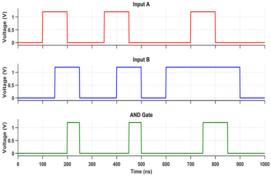
Figure 14.
Transient response of the AND gate using the proposed design.
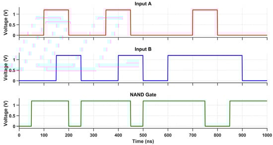
Figure 15.
Transient response of the NAND gate using the proposed design.
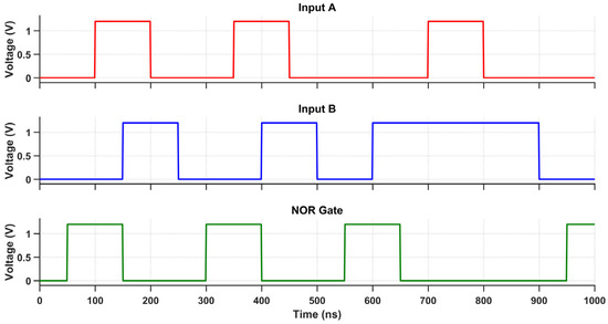
Figure 16.
Transient response of the NOR gate using the proposed design.
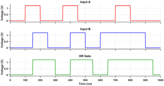
Figure 17.
Transient response of the OR gate using the proposed design.
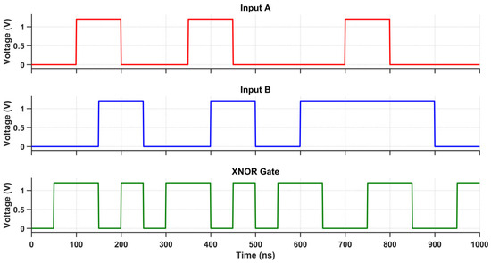
Figure 18.
Transient response of the XNOR gate using the proposed design.
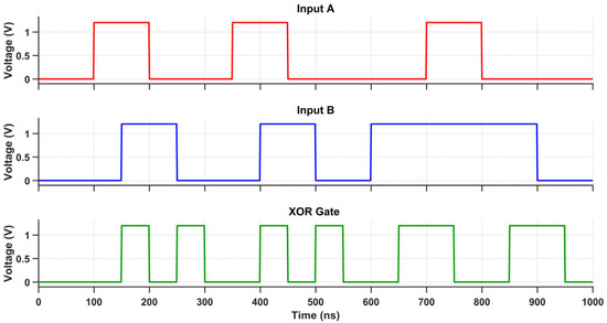
Figure 19.
Transient response of the XOR gate using the proposed design.
Monte Carlo analysis is a commonly utilized statistical simulation method in circuit design for assessing performance and reliability under diverse process, voltage, and temperature (PVT) circumstances, resulting from intrinsic manufacturing variances and environmental changes. The pronounced variances in nanoscale CMOS technology encompass temperature drifts, supply voltage instability, channel length deviations, threshold voltage fluctuations, and random device mismatches, all of which substantially affect circuit performance. Figure 20 shows a graphical representation. Monte Carlo simulations were performed to evaluate the robustness of various Boolean operations, incorporating a 30 mV sigma threshold voltage change and a ±10% deviation in nominal supply voltage (ΔVDD). The simulations were conducted under two separate temperature situations to evaluate the circuit’s resilience and operational integrity in varying thermal environments.

Figure 20.
Monte Carlo analysis of Boolean gates using the proposed design.
In Figure 21, with two datasets—an ideal MAC and a noisy MAC in the top graph, and energy consumption (red) in the bottom graph—the simulation figure compares MAC (multiply–accumulate) operations and energy consumption across 1000 operation indices. The noisy MAC shows large noise-induced fluctuations, which mimic real-world hardware flaws, such as thermal noise or quantization mistakes, whereas the ideal MAC output stays constant at 2.0. This highlights the trade-offs between accuracy and energy use in a hardware system, like a neural network accelerator. The energy consumption, measured in picojoules (pJ), fluctuates between 3000 and 3300 pJ with dips and spikes, potentially reflecting the effect of noise on computational efficiency or power management.
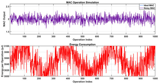
Figure 21.
Simulation result of MAC operation and energy consumption for multibit operations.
In Figure 22, three graphs examining the accuracy (in bits) trade-offs between 4 and 10 in a computational system are shown. These graphs are connected to MAC (multiply–accumulate) operations, such as neural network accelerators. Higher precision necessitates more power, as evidenced by the top graph’s (blue line) declining energy efficiency (in TOPS/W) from roughly 20 to 4 as precision rises. The MAC accuracy (as a percentage) is shown in the center graph (red line) as increasing from 99.994% at 4 bits to a steady 99.999% after 6 bits, indicating a saturation point when more precision results in negligible accuracy gains. As precision increases, the normalized area penalty increases linearly from 0 to over 30, as seen in the bottom graph (purple line), which reflects the higher demands on hardware resources.

Figure 22.
Trade-off analysis of energy efficiency, accuracy, and area penalty vs. precision in MAC operations.
Three operation modes—SRAM, Boolean, BNN, and TNN—are compared using three metrics in Figure 23. With all modes attaining roughly 80 TOPS/W, the top graph (pink bars) displays energy efficiency in TOPS/W, demonstrating constant power efficiency across SRAM, Boolean, BNN, and TNN. With all modes achieving almost 100%, the middle graph (green bars) shows MAC correctness as a percentage, indicating high and consistent computational accuracy. With all modes using roughly 3000 pJ, the bottom graph (blue bars) shows mode-switching energy in picojoules (pJ), indicating comparable energy costs for mode switching.
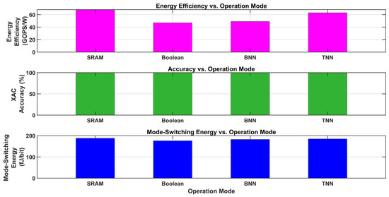
Figure 23.
Comparison of energy efficiency, accuracy, and mode-switching energy across SRAM, Boolean, BNN, and TNN operation modes.
Figure 24 presents a 3D surface plot which shows the optimal efficiency margin (objective function) as a function of threshold voltage (y-axis, which ranges from 0.32 to 0.48 V) and capacitor size (x-axis, which ranges from 0.5 × 10⁻¹⁴ to 5 × 10⁻¹⁴ F). Higher values (yellow) imply better optimization. The z-axis shows the optimized efficiency margin, with values ranging from 0.2 to 0.55. A critical balance for sense amplifier performance in hardware design is suggested by the plot, which displays a peak efficiency margin of about 0.55 at a threshold voltage of 0.38 V and a capacitor size of roughly 2 × 10⁻¹⁴ F. Efficiency decreases (blue regions) as parameters diverge from this ideal point.
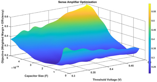
Figure 24.
Optimized efficiency margin of sense amplifier vs. capacitor size and threshold voltage.
Two time-series charts comparing sampled and optimized values across 2000 sample indices make up the Figure 25. In the top plot, “Threshold Voltage Optimization”, the y-axis displays the threshold voltage (Vth), which ranges from 0.32 to 0.48 V in volts. The orange line shows optimized Vth values, which are consistently lower and more stable, indicating an efficient optimization process, whereas the blue line shows sampled Vth values with notable oscillations. In the bottom figure, “Capacitor Size Optimization”, the y-axis shows the size of the capacitor in femtofarads (fF), which range from 0 to 45 fF. The orange line indicates optimized sizes, which are smaller and more consistent, showing increased stability and efficiency in the optimization process, whereas the magenta line displays sampling capacitor sizes with considerable variability.
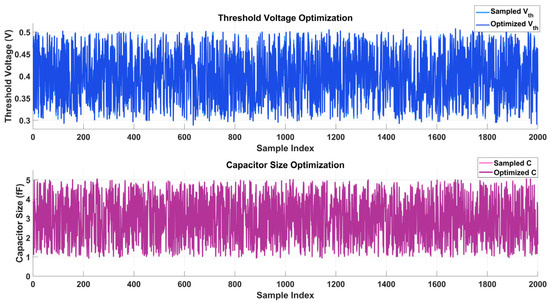
Figure 25.
Comparison of sampled vs. optimized threshold voltage and capacitor size over 2000 sample indices.
Figure 26 comprises three time-series plots evaluating the impact of error correction code (ECC) on computational performance over 1000 operation indices. The top plot (blue) shows the error correction rate as a percentage, fluctuating between 0% and 100%, with significant drops around indices 100, 300, 500, 700, and 900, indicating intermittent failures in error correction. The middle plot (red) displays MAC accuracy with ECC as a percentage, ranging from 99% to 99.98%, with notable dips aligning with the error correction drops, suggesting that failed error correction impacts computational accuracy. The bottom plot (green) illustrates energy consumption per operation in picojoules (pJ), varying between 820 and 880 pJ, with fluctuations potentially tied to ECC overhead or error correction retries.
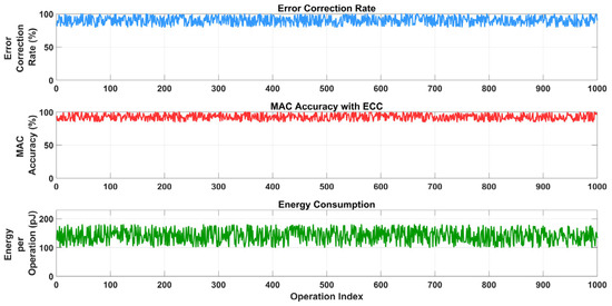
Figure 26.
Impact of error correction code (ECC) on error correction rate, MAC accuracy, and energy consumption over 1000 operation indices.
The proposed methodology extends beyond traditional ECC validation by integrating hardware-aware fault modeling to facilitate low-overhead mitigation solutions specifically designed for energy-constrained in-memory computing (IMC) systems. Unlike heavyweight error correction methods that need significant redundancy or intricate decoding logic, the (15, 11) SEC-DED Hamming ECC—enhanced with bit interleaving—attains substantial fault resilience with minimal implementation complexity. The interleaving occurs at the address-mapping level, preserving the integrity of the core SRAM cell array and maintaining compatibility with conventional foundry SRAM compilers.
The ECC logic is located in the IMC periphery, allowing correction to be independent from the core computation datapath and to function concurrently with the multi-logic sense amplifier (MLSA) readout. This architectural segregation maintains the throughput of vector-matrix multiplication (VMM) operations and prevents time interference with the primary computation pipeline.
7. Conclusions and Future Work
This study presents a resilient and scalable 8T SRAM-based in-memory computing (IMC) macro utilizing a reconfigurable capacitor array (5–80 fF) and a configurable-precision MAC engine, implemented in 45 nm CMOS technology. This combination attains an energy efficiency of 10–20 TOPS/W and exceeds 95% accuracy across 4–10 bit operations under ±5% PVT fluctuations. Dual-mode BNN/TNN functionality with XNOR-and-accumulate logic delivers 20–30 TOPS/W and exceeds 97% accuracy with a mode-switching latency of less than 5 ns. An AI-driven optimization methodology employing neural networks and genetic algorithms co-optimizes threshold voltage and capacitor size, achieving over 80 mV sensing margin and 10–15 TOPS/W efficiency across 2000 PVT-aware simulations. The sense amplifier’s implementation of in-memory Hamming code error correction, utilizing XOR logic, ensures a correction rate exceeding 99% and MAC accuracy surpassing 98% at a bit error rate of 10−3 without requiring additional hardware. This comprehensive approach addresses the limitations of fixed-precision architectures, 6T/10T SRAM cells, and analog CIM, establishing a reliable and efficient platform for edge AI inference in resource-constrained environments.
The next phase will concentrate on moving the 8T SRAM-based IMC architecture from Cadence Virtuoso simulations at 45 nm to physical prototyping, thereby bridging the gap between simulation and real-world deployment. This encompasses strategies for silicon implementation to assess layout-driven parasitics, thermal stability, process variation sensitivity, and IR drop during manufacturing, utilizing parasitic extraction and EM/IR-aware design tools. A behavioral prototype will concurrently be created on a Xilinx FPGA platform to evaluate system-level functionality, dataflow control, and AI inference under edge workloads, including UAV signal processing. The FPGA-based method will provide swift assessment of timing closure, pipeline delay, and memory access scheduling in a real-time hardware context, guaranteeing the architecture’s functional integrity and physical feasibility.
Author Contributions
Conceptualization, S.S.K. and J.N.; methodology, S.S.K.; software, S.S.K.; validation, S.S.K.; formal analysis, S.S.K.; investigation, S.S.K.; resources, S.S.K. and J.N.; data curation, S.S.K. and J.N.; writing—original draft preparation, S.S.K.; writing—review and editing, S.S.K. and J.N.; visualization, S.S.K.; supervision, J.N. All authors have read and agreed to the published version of the manuscript.
Funding
This research received no external funding.
Data Availability Statement
Dataset available on request from the authors.
Acknowledgments
The authors express their gratitude to the Department of Electrical and Electronics Engineering, BITS Pilani—Dubai Campus, U.A.E., along with the Cadence Academic Network team for providing the necessary resources to carry out the simulations required for the research.
Conflicts of Interest
The authors declare no conflicts of interest.
Abbreviations
The following abbreviations are used in this manuscript:
| IMC | In-Memory Computing |
| MLSA | Multi Logic Sense Amplifier |
| SA | Sense Amplifier |
| AI | Artificial Intelligence |
| CMOS | Complementary Metal-Oxide-Semiconductor |
| PVT | Process, Voltage, and Temperature |
| BNN | Binary Neural Network |
| TNN | Ternary Neural Network |
| CNN | Convolutional Neural Network |
| SRAM | Static Random-Access Memory |
| DRAM | Dynamic Random-Access Memory |
| RRAM | Resistive Random-Access Memory |
| MAC | Multiply and Accumulate |
| ECC | Error-Correcting Code |
| BL | Bitline |
| BLB | Bitline Bar |
| RBL | Read Bitline |
| RWL | Read Word Line |
References
- Ankit, A.; Chakraborty, I.; Agrawal, A.; Ali, M.; Roy, K. Circuits and architectures for in-memory computing-based machine learning accelerators. IEEE Micro 2020, 40, 8–22. [Google Scholar] [CrossRef]
- Ali, M.F.; Jaiswal, A.; Roy, K. In-memory low-cost bit-serial addition using commodity DRAM technology. IEEE Trans. Circuits Syst. I Reg. Pap. 2020, 67, 155–165. [Google Scholar] [CrossRef]
- Agrawal, A.; Jaiswal, A.; Roy, D.; Han, B.; Srinivasan, G.; Ankit, A. Xcel-RAM: Accelerating binary neural networks in high-throughput SRAM compute arrays. IEEE Trans. Circuits Syst. I Reg. Pap. 2019, 66, 3064–3076. [Google Scholar] [CrossRef]
- Deng, Q.; Wang, C.; Deng, Z. Memristive Circuit of Quaternion Multiplication and Its Application in Aircraft Attitude Computation. IEEE Trans. Circuits Syst. II Express Briefs 2024, 71, 3970–3974. [Google Scholar] [CrossRef]
- Nandakumar, S.R.; Le Gallo, M.; Piveteau, C.; Joshi, V.; Mariani, G.; Boybat, I.; Karunaratne, G.; Khaddam-Aljameh, R.; Egger, U.; Petropoulos, A.; et al. Mixed-Precision Deep Learning Based on Computational Memory. Front. Neurosci. 2020, 14, 406. [Google Scholar] [CrossRef]
- Zhou, Y.; Han, S.-T. Foreword to the focus issue: Materials and technologies for memristors and neuromorphic devices. Sci. Technol. Adv. Mater. 2023, 24, 2263265. [Google Scholar] [CrossRef] [PubMed]
- Cheng, C.; Tiw, P.J.; Cai, Y.; Yan, X.; Yang, Y.; Huang, R. In-memory computing with emerging nonvolatile memory devices. Sci. China Inf. Sci. 2021, 64, 221402. [Google Scholar] [CrossRef]
- Mannocci, P.; Farronato, M.; Lepri, N.; Cattaneo, L.; Glukhov, A.; Sun, Z.; Ielmini, D. In-memory computing with emerging memory devices: Status and outlook. Virtual Community Pathol. Anat. 2023, 1, 010902. [Google Scholar] [CrossRef]
- Lv, Z.; Zhu, S.; Wang, Y.; Ren, Y.; Luo, M.; Wang, H.; Zhang, G.; Zhai, Y.; Zhao, S.; Zhou, Y.; et al. Development of Bio-Voltage Operated Humidity-Sensory Neurons Comprising Self-Assembled Peptide Memristors. Adv. Mater. 2024, 36, e2405145. [Google Scholar] [CrossRef]
- Pedretti, G.; Ielmini, D. In-Memory Computing with Resistive Memory Circuits: Status and Outlook. Electronics 2021, 10, 1063. [Google Scholar] [CrossRef]
- Rashed, M.R.H.; Jha, S.K.; Yao, F.; Ewetz, R. Hybrid Digital-Digital In-Memory Computing. In Proceedings of the 2022 Design, Automation & Test in Europe Conference & Exhibition (DATE), Antwerp, Belgium, 14–23 March 2022; pp. 1177–1180. [Google Scholar] [CrossRef]
- Rasch, M.J.; Carta, F.; Fagbohungbe, O.; Gokmen, T. Fast and robust analog in-memory deep neural network training. Nat. Commun. 2024, 15, 7133. [Google Scholar] [CrossRef] [PubMed]
- Dalgaty, T.; Moro, F.; Demirağ, Y.; De Pra, A.; Indiveri, G.; Vianello, E.; Payvand, M. Mosaic: In-memory computing and routing for small-world spike-based neuromorphic systems. Nat. Commun. 2024, 15, 142. [Google Scholar] [CrossRef] [PubMed]
- Reis, D.; Geng, H.; Niemier, M.; Hu, X.S. IMCRYPTO: An In-Memory Computing Fabric for AES Encryption and Decryption. IEEE Trans. Very Large Scale Integr. (VLSI) Syst. 2022, 30, 553–565. [Google Scholar] [CrossRef]
- Joshi, P.; Rahaman, H. Memristor based In-Memory Computing for Edge AI Applications. In Proceedings of the 2023 International Symposium on Devices, Circuits and Systems (ISDCS), Higashihiroshima, Japan, 29–31 May 2023; pp. 1–6. [Google Scholar] [CrossRef]
- Ning, H.; Yu, Z.; Zhang, Q.; Wen, H.; Gao, B.; Mao, Y.; Li, Y.; Zhou, Y.; Zhou, Y.; Chen, J.; et al. An in-memory computing architecture based on a duplex two-dimensional material structure for in situ machine learning. Nat. Nanotechnol. 2023, 18, 493–500. [Google Scholar] [CrossRef]
- Lee, S.; Kim, Y. Charge-Domain Static Random Access Memory-Based In-Memory Computing with Low-Cost Multiply-and-Accumulate Operation and Energy-Efficient 7-Bit Hybrid Analog-to-Digital Converter. Electronics 2024, 13, 666. [Google Scholar] [CrossRef]
- Azougagh, D.; Rebbani, A.; Bouattane, O. Bit-line Keeper based Computational Memory Architecture: Varieties and comparisons. In Proceedings of the 2020 1st International Conference on Innovative Research in Applied Science, Engineering and Technology (IRASET), Meknes, Morocco, 19–20 March 2020; pp. 1–6. [Google Scholar] [CrossRef]
- Gu, X.; Che, R.; Dong, Y.; Yu, Z. A Novel Word Line Driver Circuit for Compute-in-Memory Based on the Floating Gate Devices. Electronics 2023, 12, 1185. [Google Scholar] [CrossRef]
- Kim, S.; Yoo, H.-J. An Overview of Computing-in-Memory Circuits With DRAM and NVM. IEEE Trans. Circuits Syst. II Express Briefs 2024, 71, 1626–1631. [Google Scholar] [CrossRef]
- Shanbhag, N.R.; Roy, S.K. Benchmarking In-Memory Computing Architectures. IEEE Open J. Solid-State Circuits Soc. 2022, 2, 288–300. [Google Scholar] [CrossRef]
- Xiao, H.; Zhao, R.; Liu, Y.; Liu, Y.; Chen, J. Bi-Directional and Operand-Controllable In-Memory Computing for Boolean Logic and Search Operations with Row and Column Directional SRAM (RC-SRAM). Micromachines 2024, 15, 1056. [Google Scholar] [CrossRef]
- Lee, K.; Cheon, S.; Jo, J.; Choi, W.; Park, J. A Charge-Sharing based 8T SRAM In-Memory Computing for Edge DNN Acceleration. In Proceedings of the 2021 58th ACM/IEEE Design Automation Conference (DAC), San Francisco, CA, USA, 5–9 December 2021; pp. 739–744. [Google Scholar] [CrossRef]
- Nguyen, V.T.; Kim, J.-S.; Lee, J.-W. 10T SRAM Computing-in-Memory Macros for Binary and Multibit MAC Operation of DNN Edge Processors. IEEE Access 2021, 9, 71262–71276. [Google Scholar] [CrossRef]
- Hu, W.; Zhang, H.; Wei, R.; Chen, Q. A Multi-Bit Quantization Low-Latency Voltage Sense Amplifier Applied in RRAM Computing-in-Memory Macro Circuits. Electronics 2024, 13, 356. [Google Scholar] [CrossRef]
- Soundrapandiyan, K.; Vishvakarma, S.K.; Reniwal, B.S. Enabling Energy-Efficient In-Memory Computing With Robust Assist-Based Reconfigurable Sense Amplifier in SRAM Array. IEEE J. Emerg. Sel. Top. Circuits Syst. 2023, 13, 445–455. [Google Scholar] [CrossRef]
- An, B.-K.; Zhang, X.; Do, A.T.; Kim, T.T.-H. Design of a Current Sense Amplifier with Dynamic Reference for Reliable Resistive Memory. In Proceedings of the 2023 21st IEEE Interregional NEWCAS Conference (NEWCAS), Edinburgh, UK, 26–28 June 2023; pp. 1–5. [Google Scholar] [CrossRef]
- Kulkarni, P.; Goel, A.; Ndai, P.; Roy, K. A read-disturb-free, differential sensing 1r/1w port, 8t bitcell array. IEEE Trans. Very Large Scale Integr. (VLSI) Syst. 2011, 19, 1727. [Google Scholar] [CrossRef]
- Valavi, H.; Ramadge, P.J.; Nestler, E.; Verma, N. A 64-Tile 2.4-Mb In-Memory-Computing CNN Accelerator Employing Charge-Domain Compute. IEEE J. Solid-State Circuits 2019, 54, 1789–1799. [Google Scholar] [CrossRef]
- Bharti, P.K.; Jain, S.; Pillai, K.R.; Sayyaparaju, S.V.; Kalsi, G.S.; Mekie, J.; Subramoney, S. Compute-In-Memory Using 6T SRAM for a Wide Variety of Workloads. In Proceedings of the 2022 IEEE International Symposium on Circuits and Systems (ISCAS), Austin, TX, USA, 28 May–1 June 2022; pp. 2963–2967. [Google Scholar] [CrossRef]
- H. Kim, J. A 1-16b Reconfigurable 80Kb 7T SRAM-Based Digital Near-Memory Computing Macro for Processing Neural Networks. IEEE Trans. Circuits Syst. I Regul. Pap. 2023, 70, 1580–1590. [Google Scholar] [CrossRef]
- Zidan, M.A.; Strachan, J.P.; Lu, W.D. The future of electronics based on memristive systems. Nat. Electron. 2018, 1, 22–29. [Google Scholar] [CrossRef]
- Sebastian, A.; Le Gallo, M.; Khaddam-Aljameh, R.; Eleftheriou, E. Memory devices and applications for in-memory computing. Nat. Nanotechnol. 2020, 15, 529–544. [Google Scholar] [CrossRef]
- Fujiki, Y.; Mahlke, S.; Das, R. In-Memory Data Parallel Processor. In Proceedings of the Twenty-Third International Conference on Architectural Support for Programming Languages and Operating Systems, Williamsburg, VA, USA, 2–28 March 2018. [Google Scholar] [CrossRef]
- Li, P.; Parashar, A.; Pellauer, M.; Wang, T.; Emer, J. A Hierarchical Architectural Framework for Reconfigurable Logic Computing. In Proceedings of the 2013 IEEE International Symposium on Parallel & Distributed Processing, Workshops and Phd Forum, Cambridge, MA, USA, 20–24 May 2013; pp. 287–292. [Google Scholar] [CrossRef]
- Agrawal, A.; Jaiswal, A.; Lee, C.; Roy, K. X-SRAM: Enabling In-Memory Boolean Computations in CMOS Static Random-Access Memories. IEEE Trans. Circuits Syst. I Regul. Pap. 2018, 65, 4219–4232. [Google Scholar] [CrossRef]
- Han, J.; Kim, Y. A Fast Half Adder using 8T SRAM for Computation-in-Memory. In Proceedings of the 2021 IEEE International Conference on Consumer Electronics-Asia (ICCE-Asia), Gangwon, Republic of Korea, 1–3 November 2021; pp. 1–3. [Google Scholar]
- Prasad, K.; Srivastava, A.; Baruah, N.; Mekie, J. Fast and Robust Sense Amplifier for Digital In-Memory Computing. In Proceedings of the 2023 36th International Conference on VLSI Design and 2023 22nd International Conference on Embedded Systems (VLSID), Hyderabad, India, 8–12 January 2023; pp. 258–263. [Google Scholar] [CrossRef]
- Iqbal, B.; Grover, A.; Rawat, H. A Common Mode Insensitive Process Tolerant Sense Amplifier Design for In-Memory Compute Applications in 65nm LSTP Technology. In Proceedings of the 2023 36th International Conference on VLSI Design and 2023 22nd International Conference on Embedded Systems (VLSID), Hyderabad, India, 8–12 January 2023; pp. 121–126. [Google Scholar] [CrossRef]
- Chang, Y.J.; Chen, S.H. Multi-Logic Sense Amplifier (MLSA) Design for In-Memory Computing. IEEE J. Emerg. Sel. Top. Circuits Syst. 2023, 13, 371–381. [Google Scholar] [CrossRef]
- Rajput, K.; Pattanaik, M. Implementation of Boolean and Arithmetic Functions with 8T SRAM Cell for In-Memory Computation. In Proceedings of the 2020 International Conference for Emerging Technology (INCET), Belgaum, India, 5–7 June 2020; pp. 1–5. [Google Scholar] [CrossRef]
- Antolini, A.; Lico, A.; Zavalloni, F.; Scarselli, E.F.; Gnudi, A.; Torres, M.L.; Canegallo, R.; Pasotti, M. A Readout Scheme for PCM-Based Analog In-Memory Computing With Drift Compensation Through Reference Conductance Tracking. IEEE Open J. Solid-State Circuits Soc. 2024, 4, 69–82. [Google Scholar] [CrossRef]
- Moorthii, J.C.; Mourya, M.V.; Bansal, H.; Verma, D.; Suri, M. RRAM IMC based Efficient Analog Carry Propagation and Multi-bit MVM. In Proceedings of the 2024 8th IEEE Electron Devices Technology & Manufacturing Conference (EDTM), Bangalore, India, 3–6 March 2024; pp. 1–3. [Google Scholar] [CrossRef]
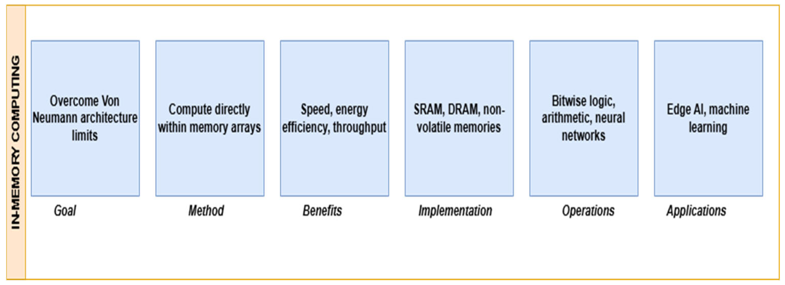
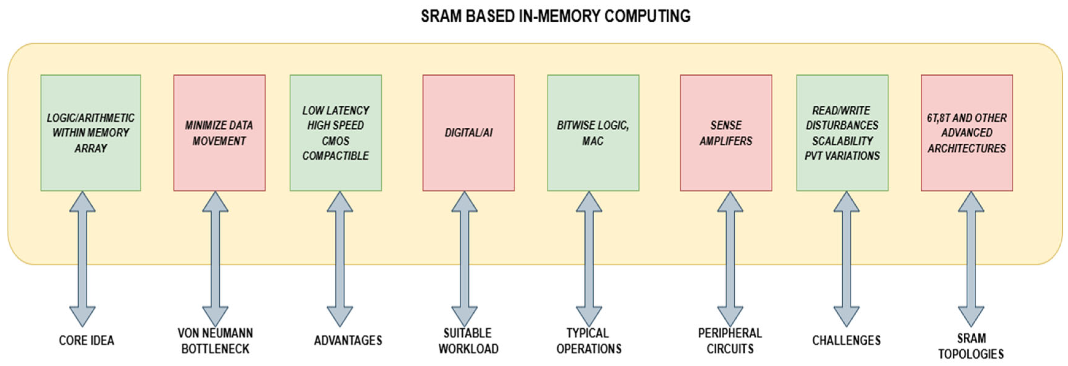
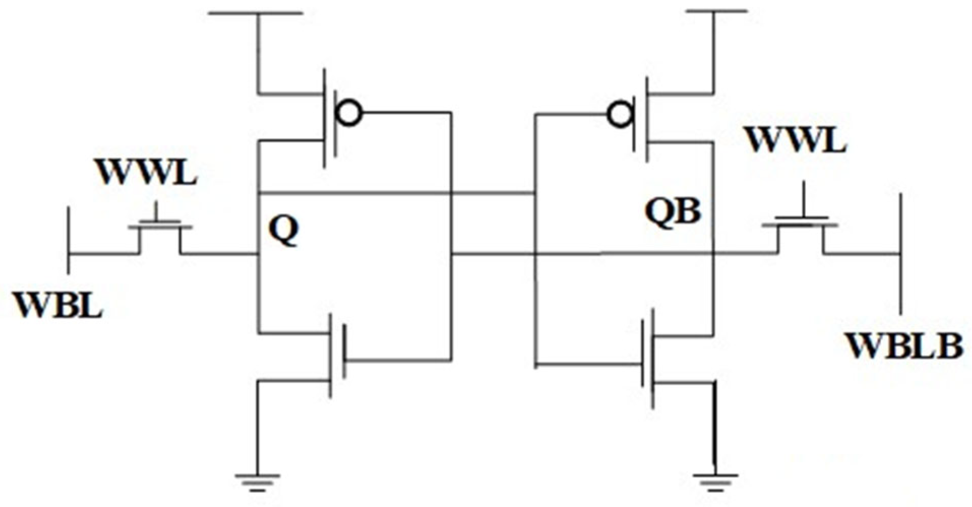
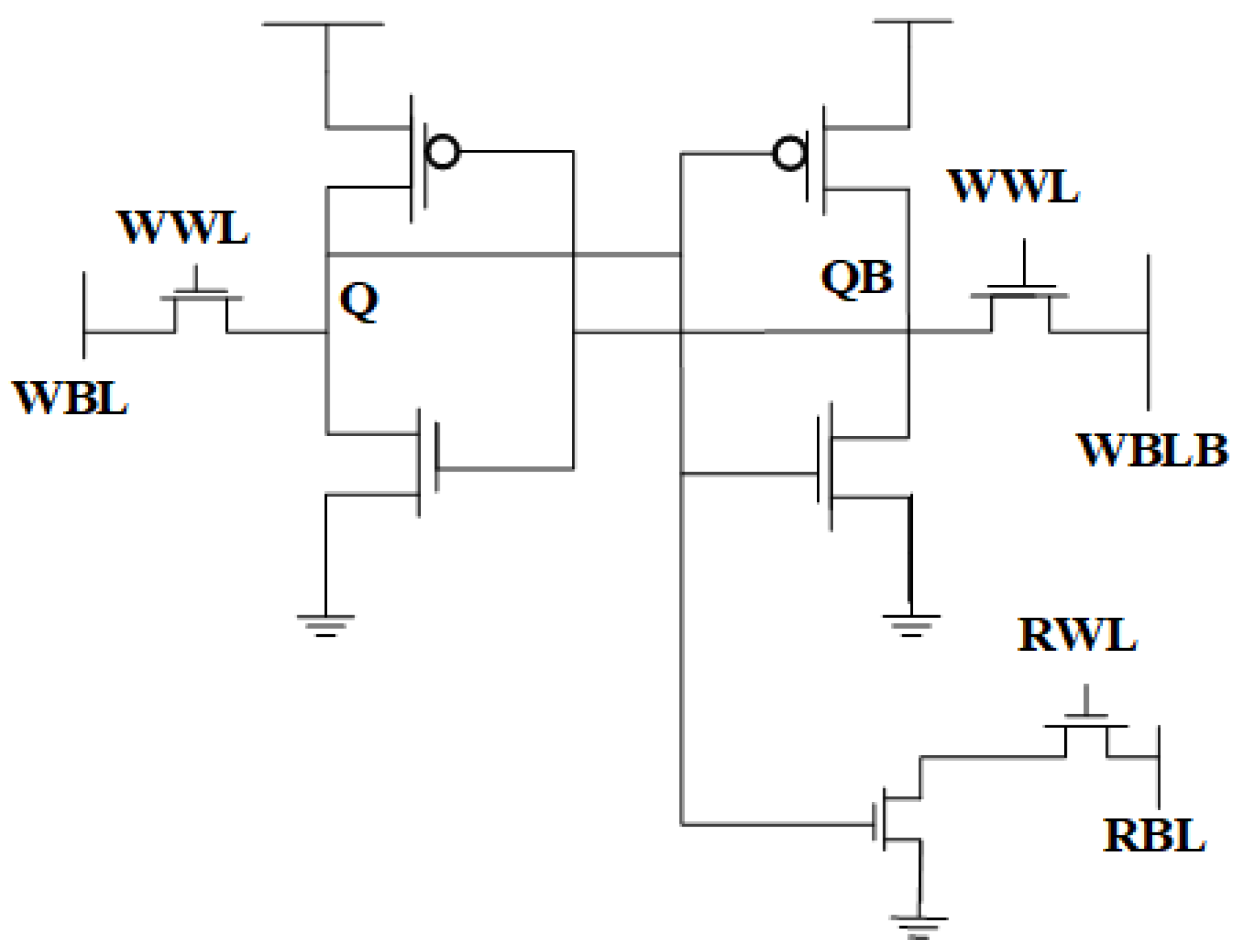
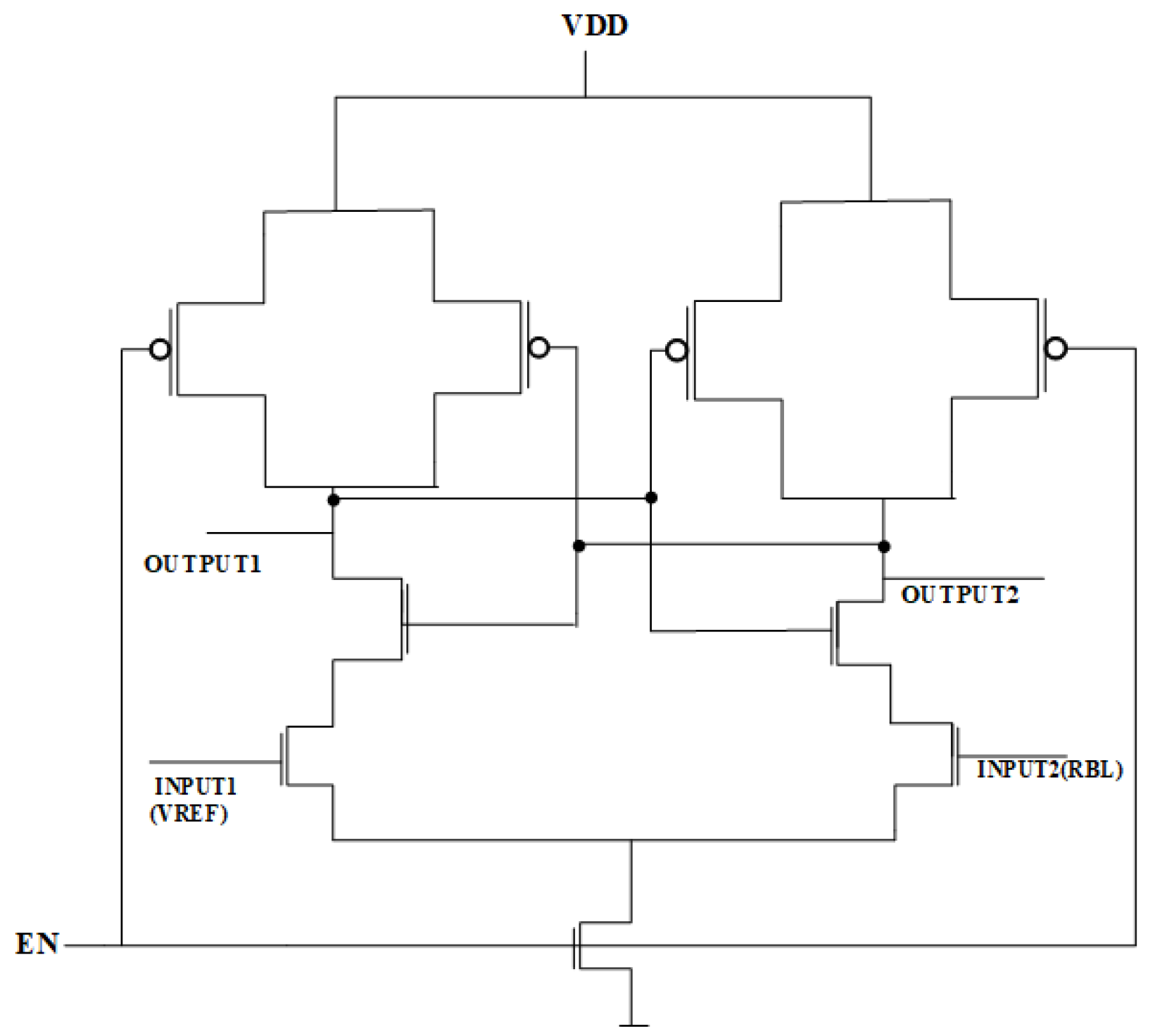
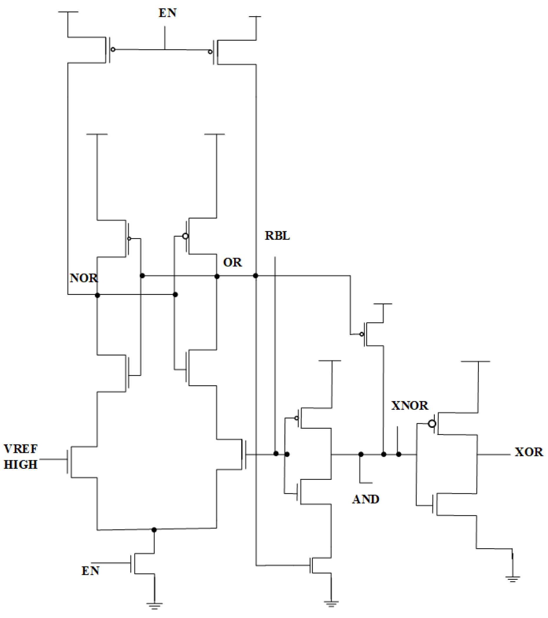
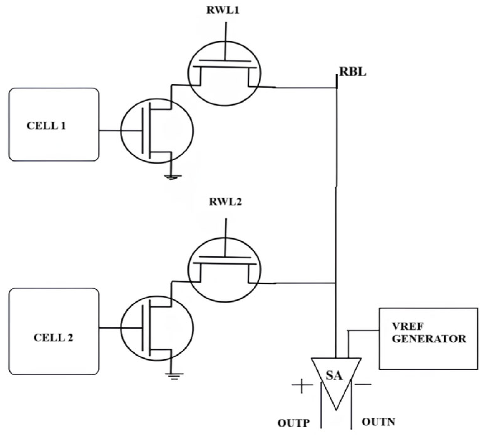
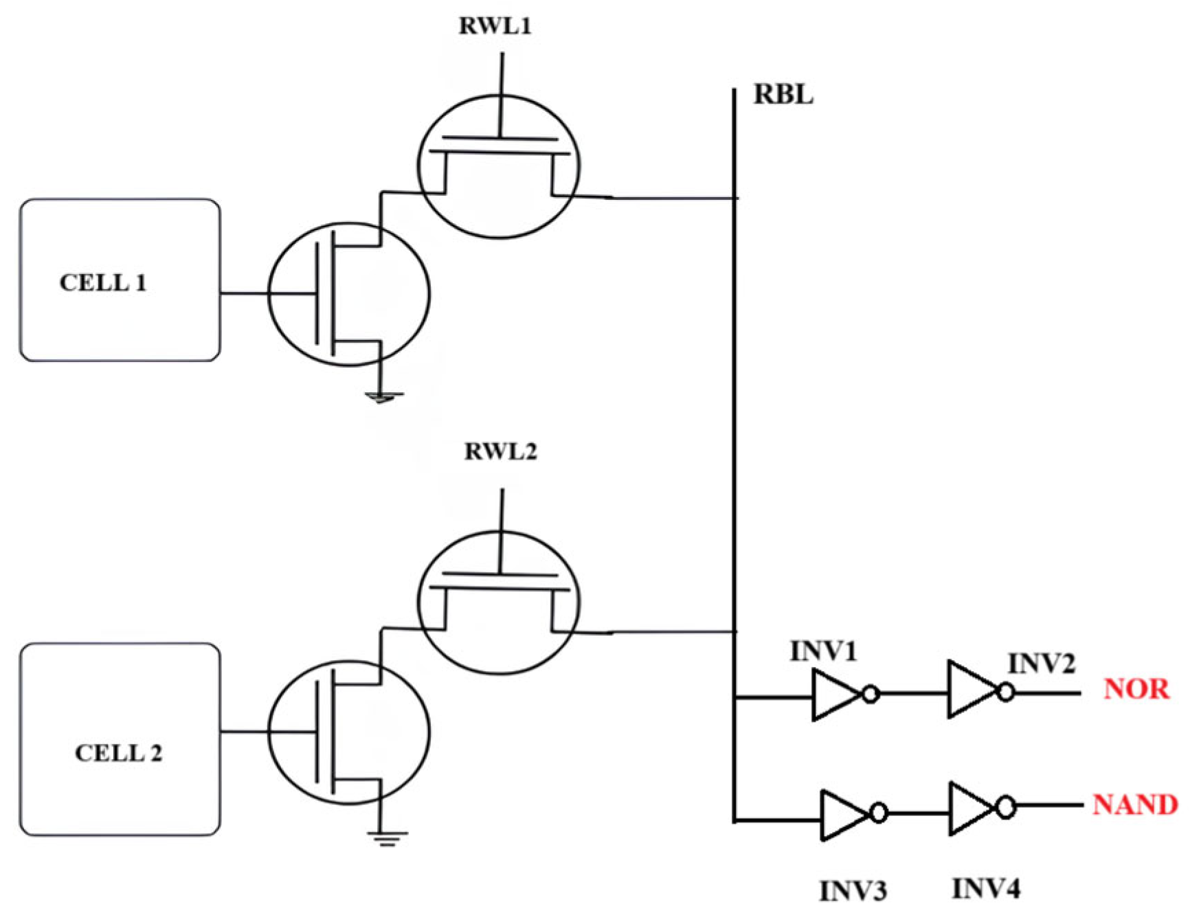

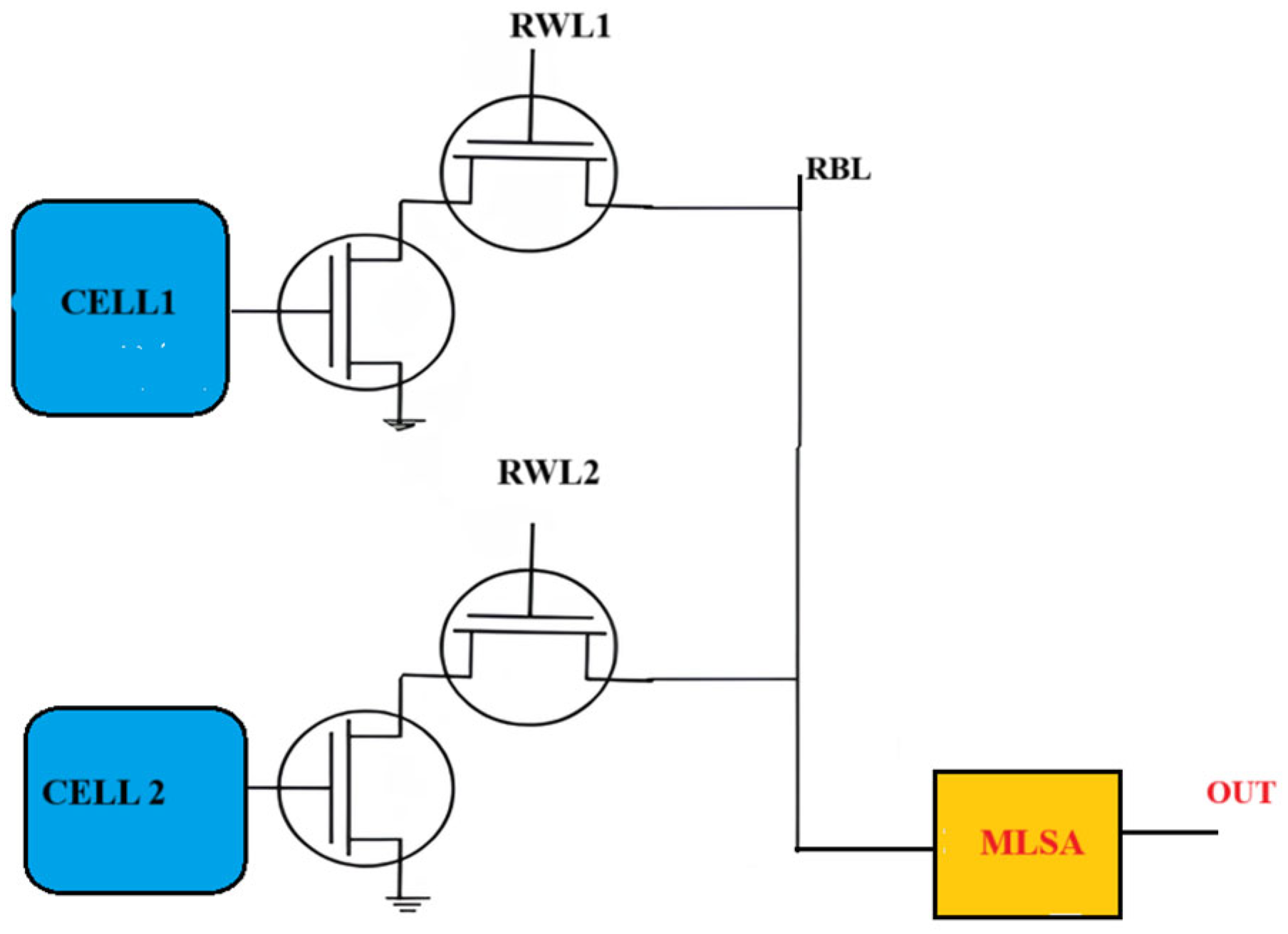
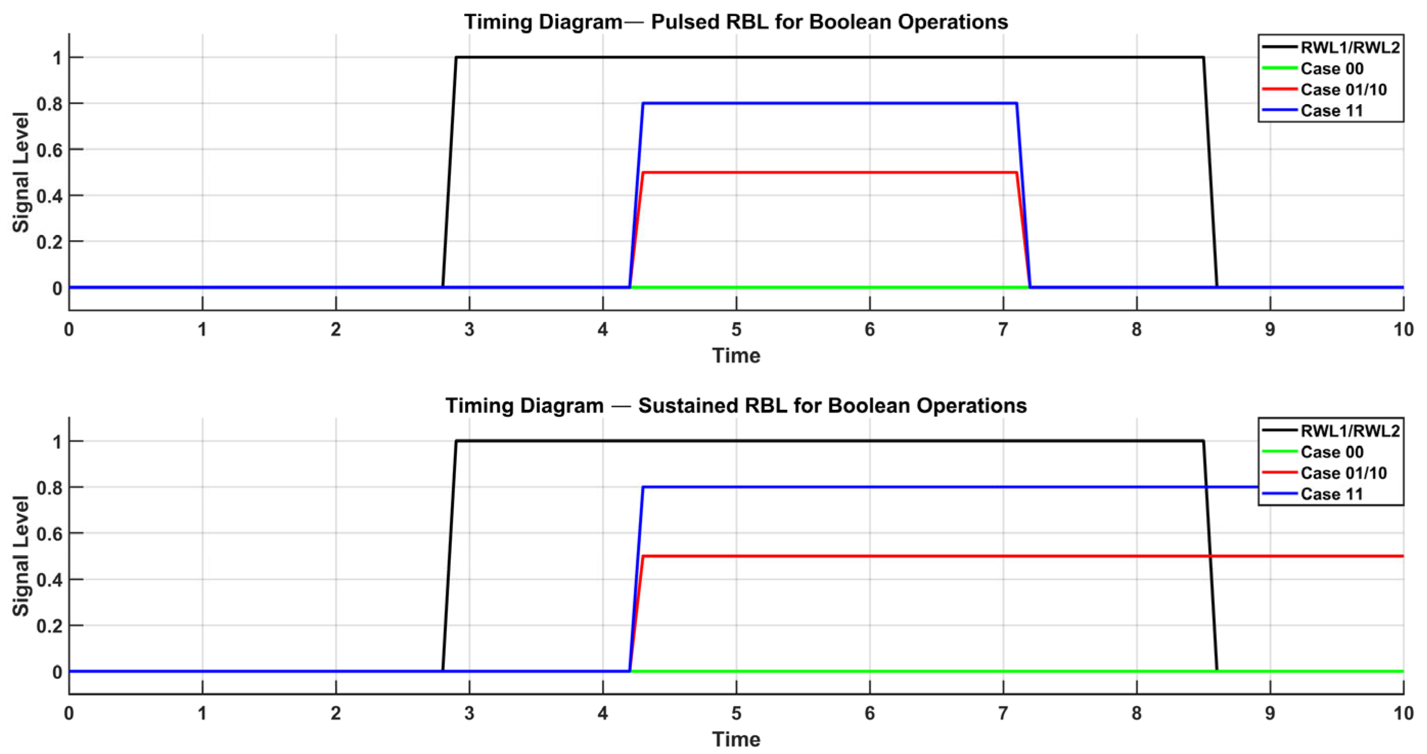
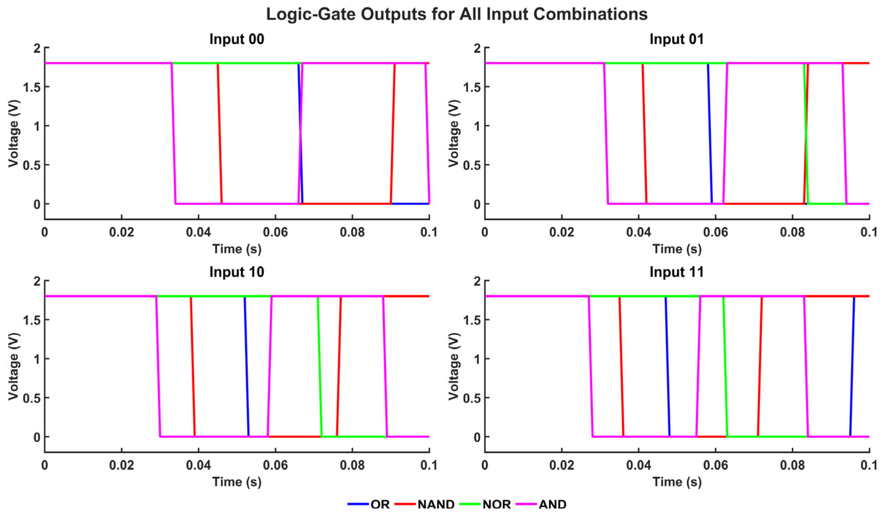
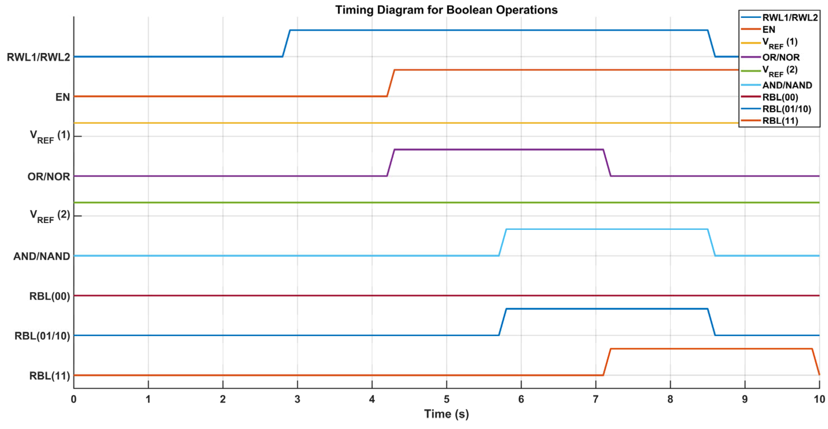
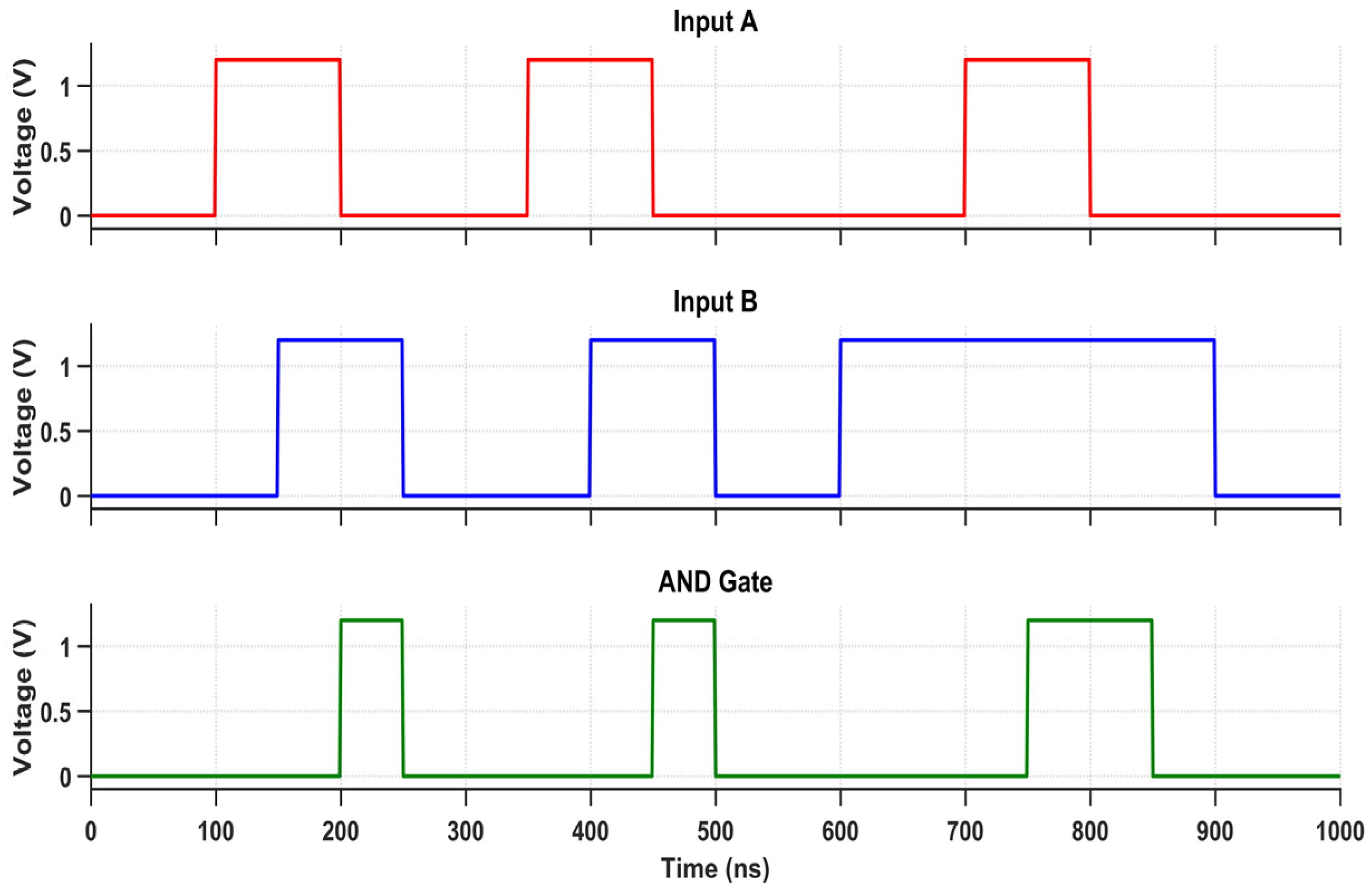
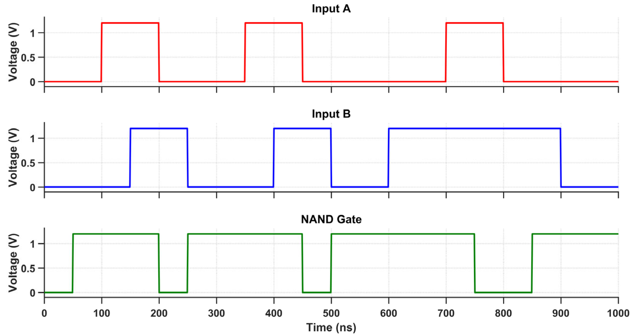
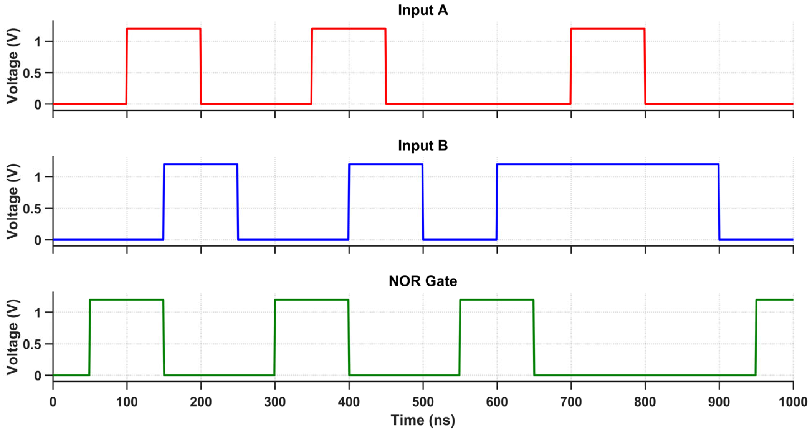
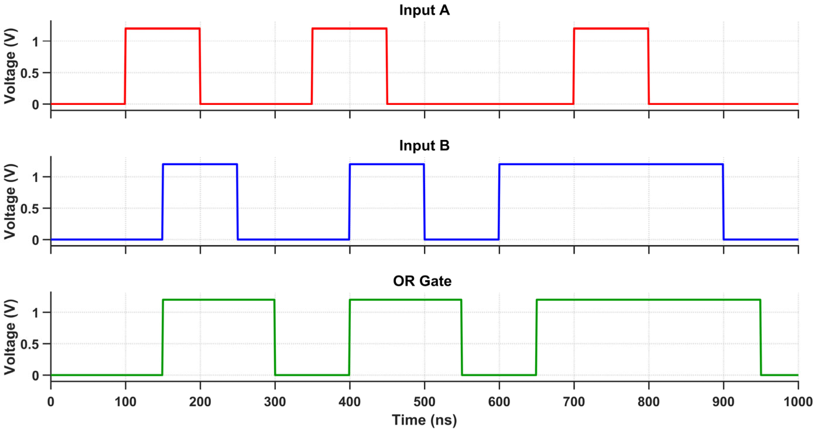
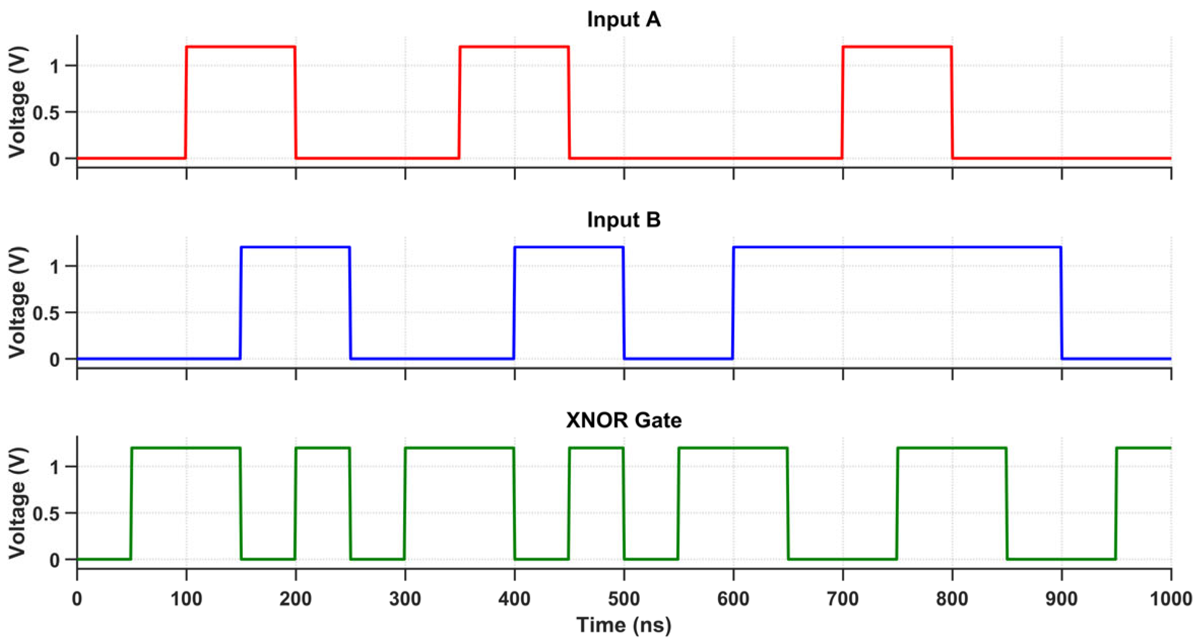
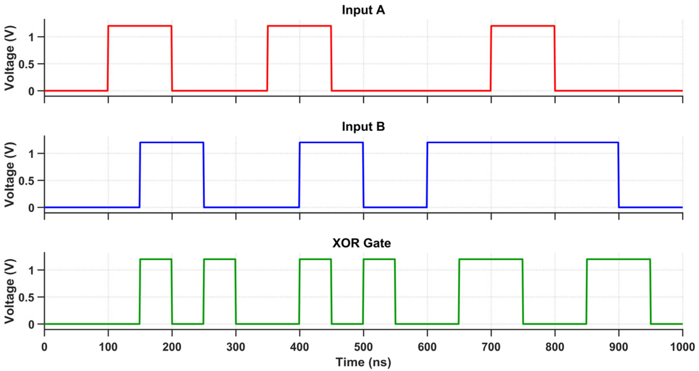
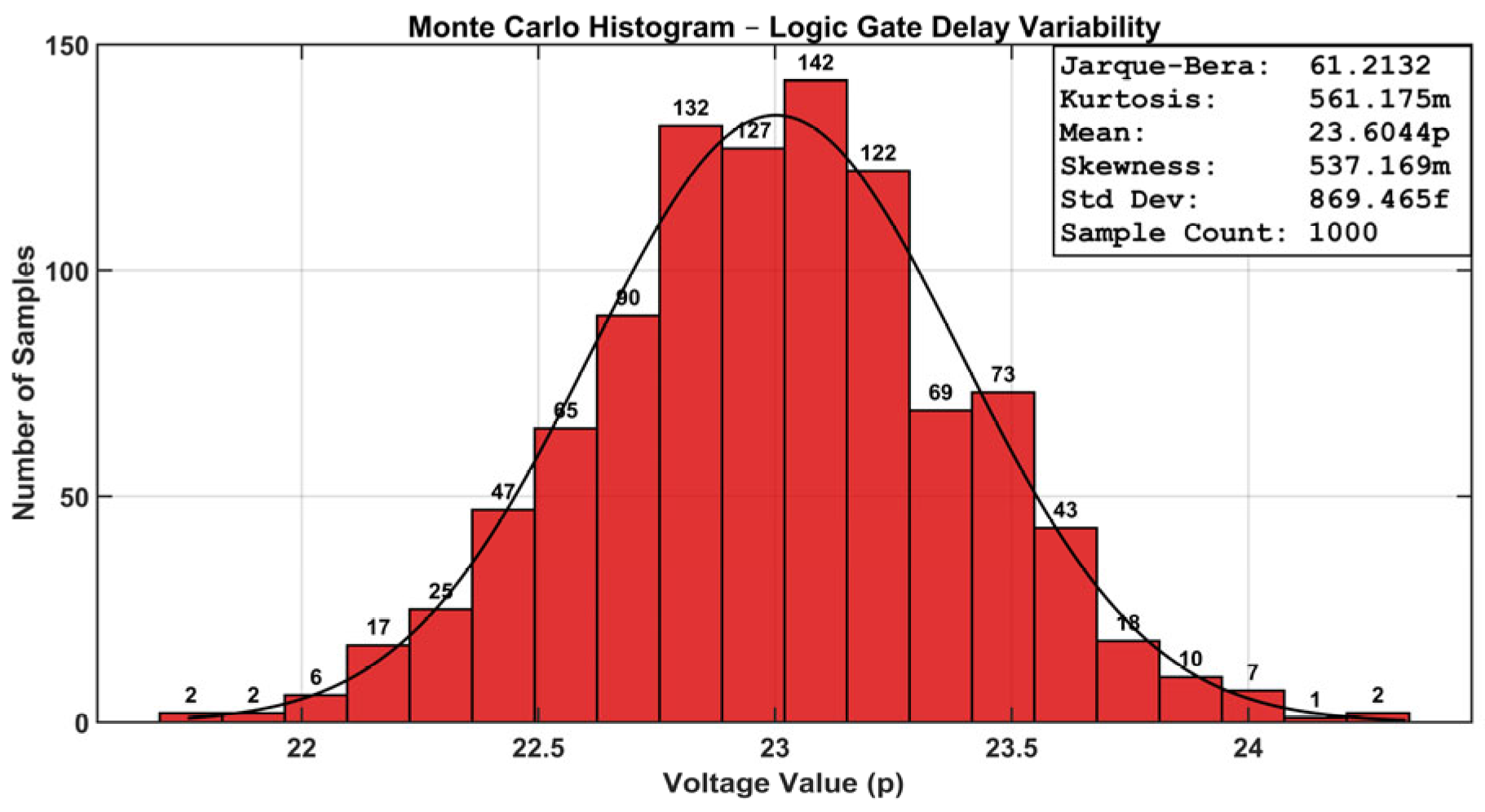
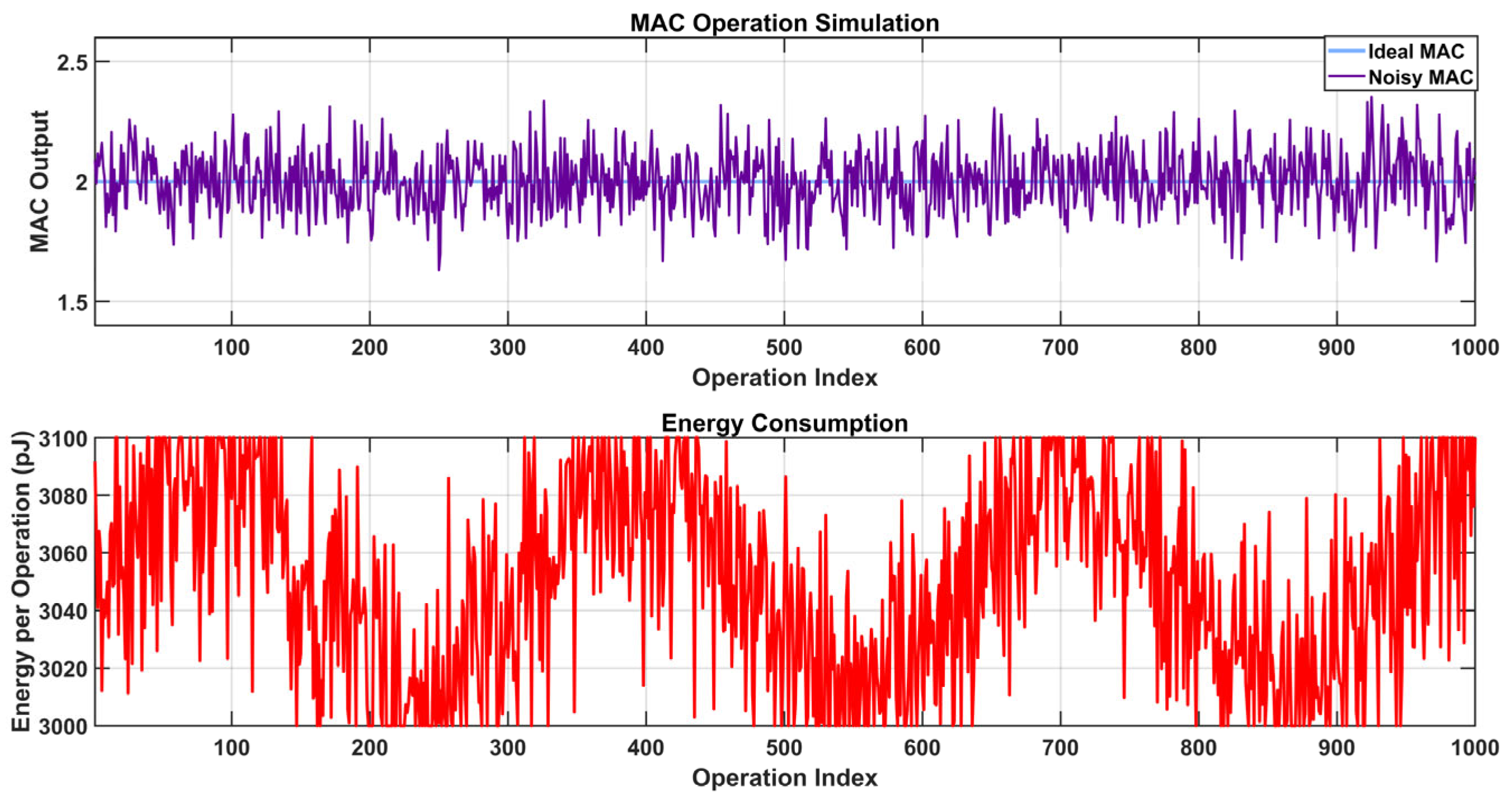
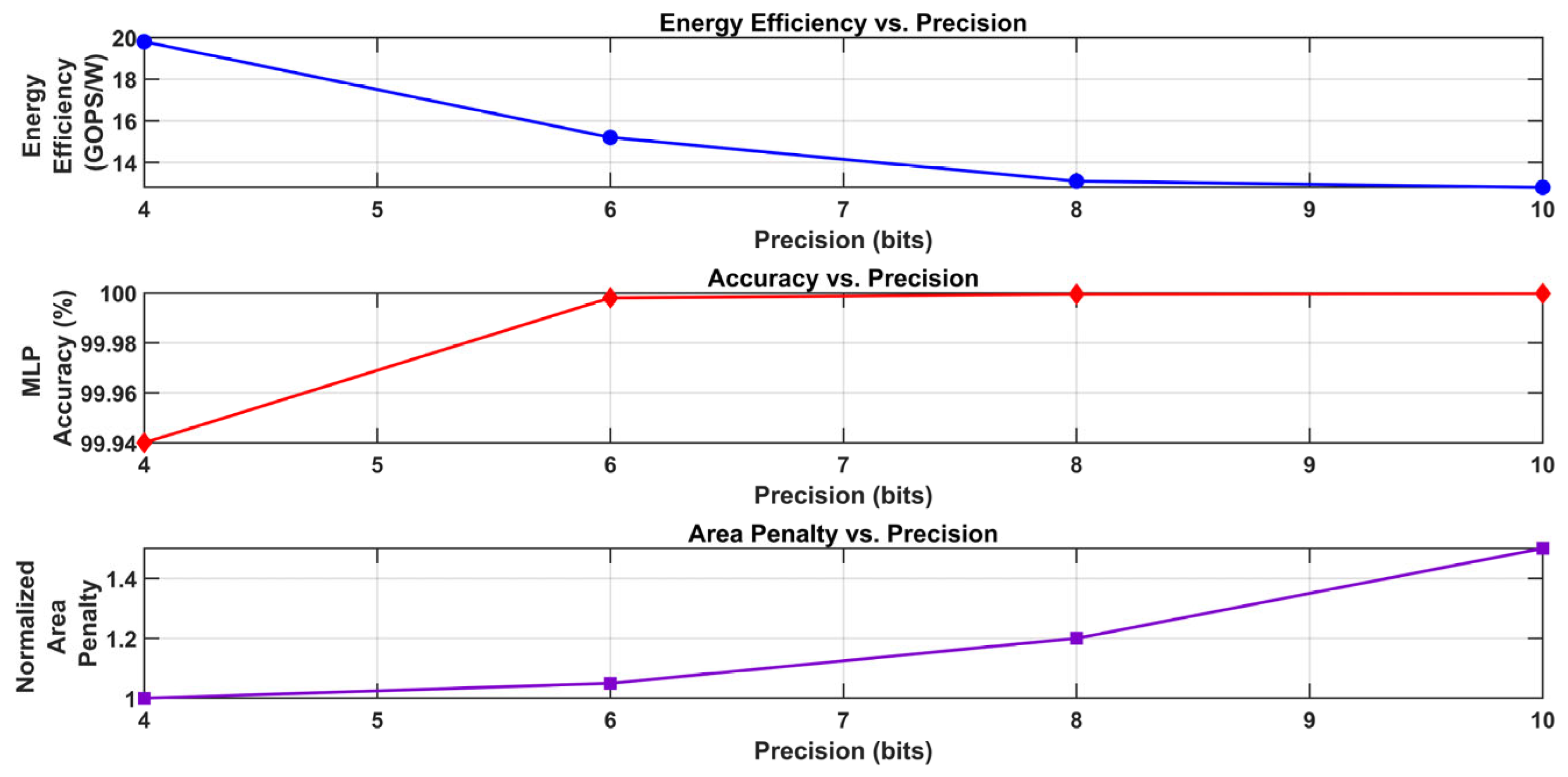

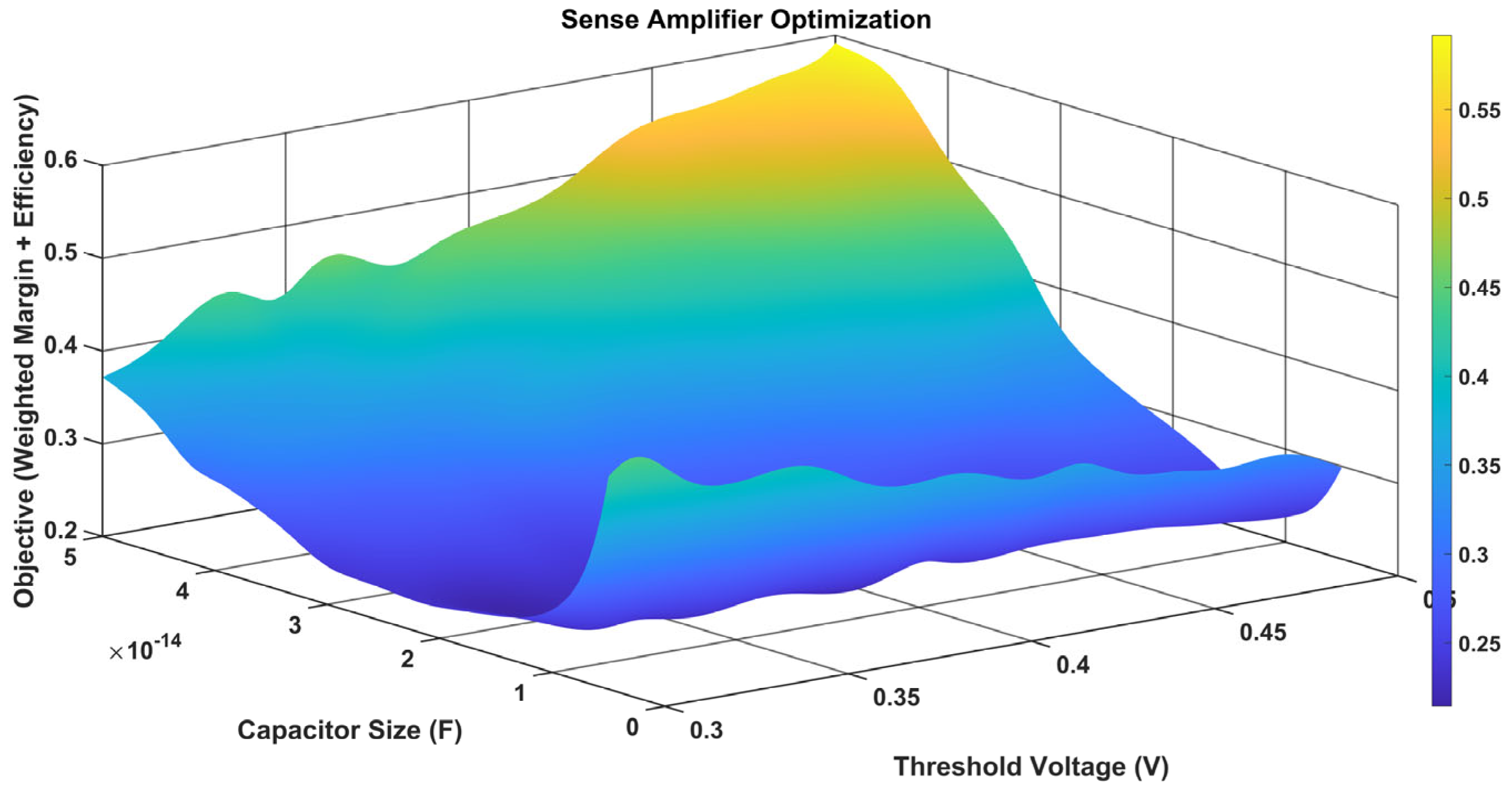

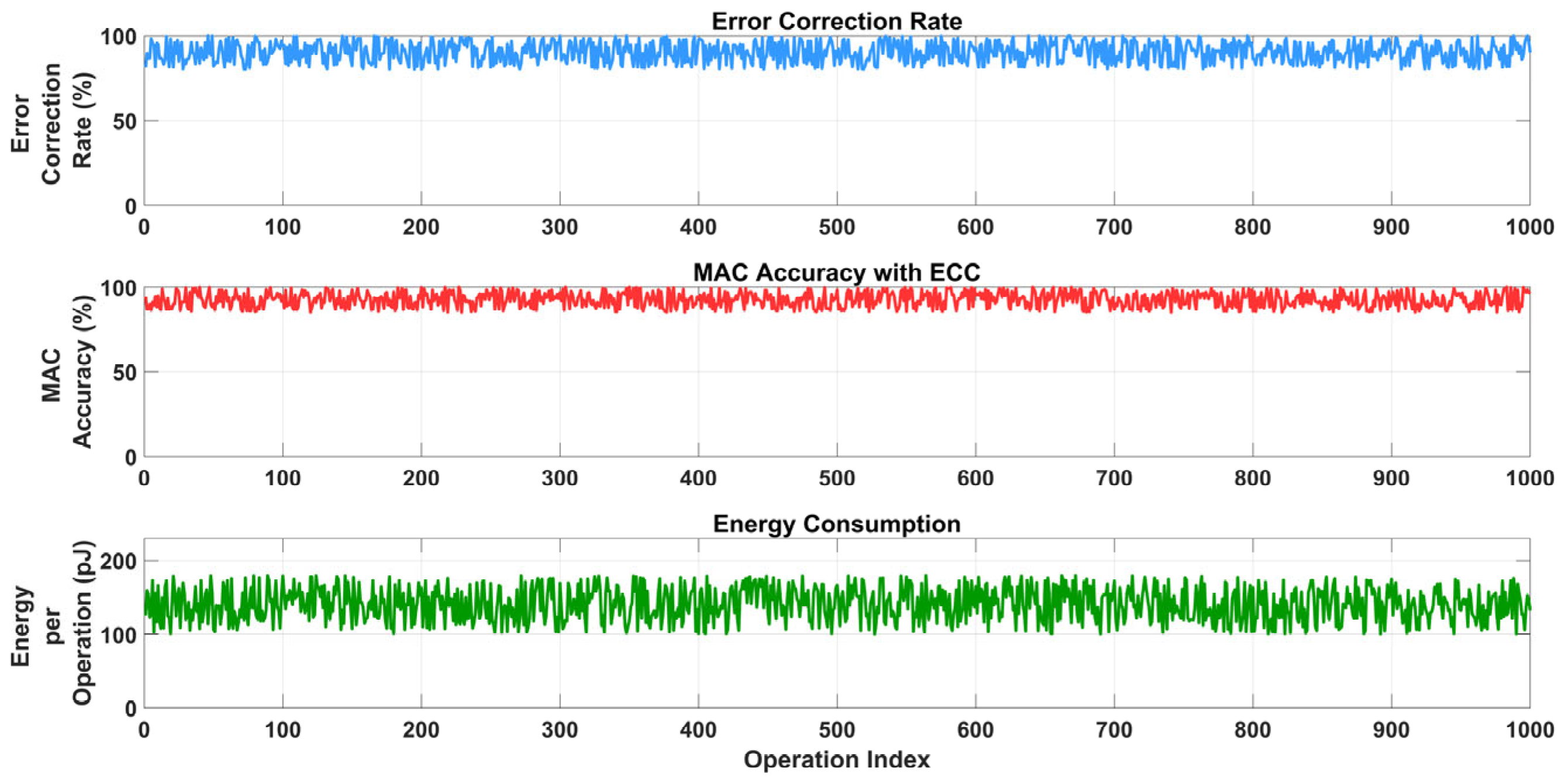
Disclaimer/Publisher’s Note: The statements, opinions and data contained in all publications are solely those of the individual author(s) and contributor(s) and not of MDPI and/or the editor(s). MDPI and/or the editor(s) disclaim responsibility for any injury to people or property resulting from any ideas, methods, instructions or products referred to in the content. |
© 2025 by the authors. Licensee MDPI, Basel, Switzerland. This article is an open access article distributed under the terms and conditions of the Creative Commons Attribution (CC BY) license (https://creativecommons.org/licenses/by/4.0/).