Article

A CMOS Current Reference with Novel Temperature Compensation Based on Geometry-Dependent Threshold Voltage Effects

by
Francesco Gagliardi
*,
Andrea Ria
,
Massimo Piotto
and
Paolo Bruschi
Department of Information Engineering, University of Pisa, 56122 Pisa, Italy
*
Author to whom correspondence should be addressed.
Electronics 2025, 14(13), 2698; https://doi.org/10.3390/electronics14132698
Submission received: 23 May 2025 / Revised: 28 June 2025 / Accepted: 2 July 2025 / Published: 3 July 2025
(This article belongs to the Section Microelectronics)

Abstract

Next-generation smart sensing devices necessitate on-chip integration of power-efficient reference circuits. The latters are required to provide other circuit blocks with highly reliable bias signals, even in the presence of temperature shifts and supply voltage disturbances, while draining a small fraction of the overall power budget. In particular, it is especially challenging to design current references with enhanced robustness and efficiency; hence, thorough exploration of novel architectures and design approaches is needed for this type of circuits. In this work, we propose a novel CMOS-only current reference, achieving temperature compensation by exploiting geometry dependences of the threshold voltage (specifically, the reverse short-channel effect and the narrow-channel effect). This allows reaching first-order temperature compensation within a single current reference core. Implemented in 0.18 µm CMOS, a version of the proposed current reference designed to deliver 141 nA (with 377 nW of total power consumption) achieved an average temperature coefficient equal to 194 ppm/°C (from −20 °C to 80 °C) and an average line sensitivity of −0.017%/V across post-layout statistical Monte Carlo simulations. Based on such findings, the newly proposed design methodology stands out as a noteworthy solution to design robust current references for power-constrained mixed-signal systems-on-chip.

1. Introduction

In the last decade, the Integrated Circuit (IC) research community has devoted increasingly greater efforts to developing novel system-on-chip (SoC) solutions for smart sensing, biomedical monitoring, and Internet-of-Things (IoT) applications [1,2,3,4]. In this respect, recent SoC designs feature a high degree of integration between analog and digital circuits, to deploy accurate sensing, in situ data processing, and wireless communication capabilities. To enable the production of miniaturized wearable/implantable devices and sensor nodes, often supplied by ultralow-capacity batteries or energy-harvesters [5,6], minimization of power consumption has emerged as a crucial need [7,8,9,10,11,12,13]. In addition, to enable reliable operation under a variety of operating conditions, strong interest has arisen in developing low-power, robust reference circuits [14,15,16,17,18,19,20]. Correct biasing of all circuit blocks within an SoC usually relies on voltage references (VRs) and current references (CRs) integrated on the same chip.
Development of VRs began very early in the history of electronics, driven by the need for stable power supplies. Furthermore, they are routinely used with non-ratiometric voltage-mode Analog-to-Digital Converters (ADCs) and Digital-to-Analog Converters (DACs). Similarly, CRs play the same role for current-mode data converters, mainly employed in telecommunication [21] and Electrical Impedance Spectroscopy (EIS) systems [22]. Moreover, the usefulness of CRs extends to a much wider category of analog cells [23]. Indeed, the thermal noise and bandwidth performances of amplifiers are strictly related to the bias current of active devices, which can be easily derived by a single accurate reference current. In addition, relaxation oscillators based on the charging and/or discharging of capacitors by means of constant currents [24,25] are receiving an increasing interest for low-power applications, where traditional RC oscillators have become unfeasibly large. It is worth noting that, in a CMOS technology, adjusting current sources can be easily accomplished by means of digitally programmable current mirrors, avoiding the use of resistors. This property allows compensation for process spread in CRs in an arguably easier way than in VRs, while low sensitivity to temperature and supply voltage variations remain a key specification.
Compared to the VR case, temperature stabilization of CRs is currently more challenging. In both cases, the general strategy implies combining Positive-Temperature-Coefficient (PTC) and Negative-Temperature-Coefficient (NTC) quantities to accomplish first-order temperature compensation. However, in the current domain, quantities available for this purpose generally show much worse linearity with respect to temperature, typically featuring power-law behaviors (i.e., I T α ). Voltage-to-current conversion might be an effective solution, but resistor-based implementations are generally inconvenient, due to the large areas needed to reach low power levels and because of the typically large global process variations of integrated resistors. All things considered, the best-performing CRs presently achieve temperature coefficient (TC) values that are 1–2 orders of magnitude larger than state-of-the-art VRs. Thereby, novel temperature stabilization approaches, compliant with low-power specifications, are continuously sought for CRs.
In this work, we present a novel CMOS-only CR circuit, achieving minimal sensitivity to temperature and supply voltage variations with low area occupation. A modified Beta-Multiplier (BM) structure is proposed, improving an architecture previously reported in [26] through the addition of a new temperature compensation and a line sensitivity (LS) minimization technique. Specifically, to achieve temperature compensation, we propose exploiting dependences of the threshold voltage ( V t h ) to geometrical dimensions of MOS transistors to derive an NTC effect, which is useful for shaping the temperature behavior of the reference current, I R E F . Prior works mostly proposed combining the outputs of separate PTC and NTC current generators [26,27] and/or leveraged body effects [26,28,29,30,31] to modulate the temperature trend of I R E F .
Ref. [26] presented CRs based on modified BM structures where temperature dependence is shaped by means of asymmetric body effects acting on transistors of a p-type non-linear current mirror (i.e., one transistor is not affected by body effects, being biased with zero body-source voltage, V B S = 0 , while the other has V B S > 0 ). In [30], this concept has been extended by introducing, on one branch of the non-linear mirror, transistors with and without body effects, connected in parallel, to allow for fine tuning of the temperature dependence by acting on the ratio between their transconductance factors. Forward Body-Biasing (FBB) has also been used in [29], demonstrating temperature compensation capabilities by linking the reference current to a diode-connected NMOS transistor with gate, drain, and body terminals all shorted together; however, this topology necessitates an auxiliary amplifier to close the feedback loop. The authors of [31] again relied on FBB, by biasing the body terminal of an NMOS device within a peaking CR topology using the output of a two-transistor VR; nevertheless, access to body terminals of NMOS devices is feasible only in triple-well CMOS processes.
The option of exploiting geometry-dependent threshold voltage effects in CRs has been scarcely explored, with [32] being the only reference, to the best of our knowledge, optimizing single transistor dimensions to improve the performance of a CR. In [32], a Proportional-To-Absolute-Temperature (PTAT) CR is presented, implemented as a BM structure using a triode-biased transistor as a source-degeneration element. To generate the gate voltage of the triode transistor, the authors used VR cells comprising long-channel and short-channel devices coupled together, with the aim of exploiting the geometry-related V t h difference as a tracking factor of global process variations. Furthermore, in the context of VR design, seminal works such as [33,34] have recently introduced the concept of optimizing device ratios within Self-Cascoded MOSFETs (SCMs) to tune not only temperature dependence but also sensitivity to global process variations. Specifically, temperature dependence can be adjusted by acting on the aspect ratios, as in standard SCM-VR designs, while process sensitivity is minimized by separately optimizing channel length values. However, these approaches fundamentally differ from the one herein proposed, which aims to minimize the temperature sensitivity of a BM-CR by introducing an NTC voltage term consisting of a threshold voltage difference due to width and length imbalances within a pair of transistors; by combining this term with a PTC voltage quantity and adopting optimal weights, the temperature sensitivity of the current within the BM loop can be ultimately minimized.
Regarding LS, we introduced a technique relying on an additional circuit branch, which is able to stabilize V D S voltages through a negative feedback. This solution has been inspired by techniques recently used in VRs [35,36] and shares similarities with the approach used in [37] for a resistor-based peaking CR. While other works simply implemented BM structures with cascode current mirrors [32,38,39,40,41,42] or amplifier-assisted regulated mirrors [43,44], the presented solution shows great potential for enhancing immunity against V d d variations at the cost of a reasonably small increase in power consumption, around 12.5%.
The remainder of this paper is organized as follows: In Section 2, we introduce the proposed CR architecture and a detailed analytical model to prove its temperature compensation capability. Then, in Section 3, we validate the presented circuit techniques by means of accurate electrical simulations of a 0.18 µm CMOS design. Finally, Section 4 compares our findings with those of prior works.

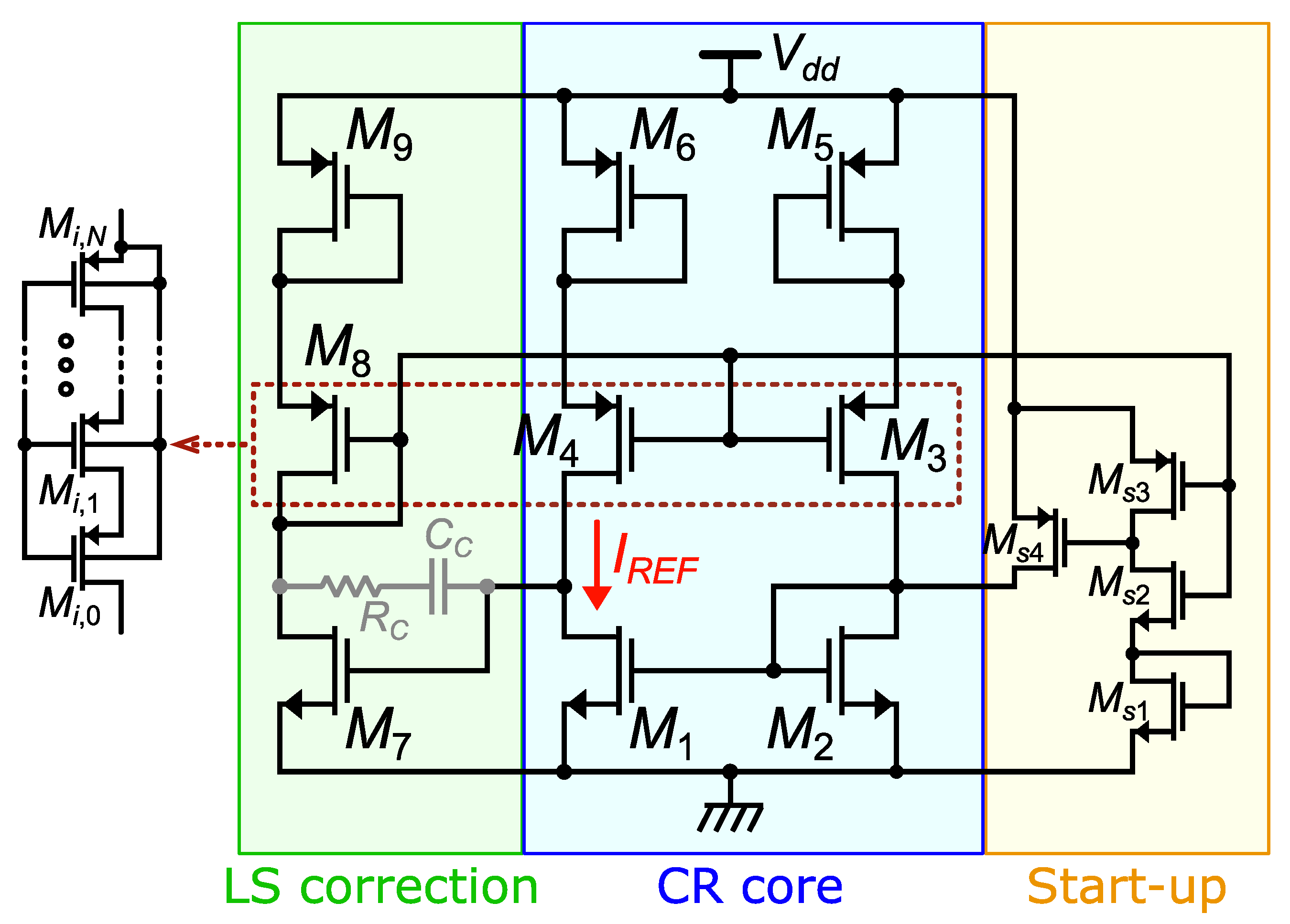
2. Proposed Architecture

2.1. Current Reference Core

Figure 1 shows a simplified version of the proposed CR, including only the core circuit needed to perform temperature compensation. The complete CR architecture, comprising also auxiliary circuits for LS correction and start-up purposes, is later discussed at the end of this section. The modified BM structure of Figure 1 was first introduced in [26], with transistors M 3 , 4 and M 5 , 6 biased in strong inversion and weak inversion, respectively. In addition, in [26], transistor pairs M 1 , 2 , M 3 , 4 , and M 5 , 6 were designed with matched channel widths and lengths, while the ratios between their aspect ratios, k = ρ 2 / ρ 1 , h = ρ 3 / ρ 4 , and u = ρ 6 / ρ 5 , were imposed by acting only on the multiplicity factors (we assume the aspect ratio of each transistor to be defined as ρ i = m i W i / L i , where m i , W i , and L i stand for the multiplicity factor, the channel width, and the channel length of M i )—regarding the choice of parameters k, h, and u, the existence of a stable dc operating point of the considered circuit is ensured by the following condition: k > max ( h / u , 1 / u ) [26].
It is worth noting that, as far as the geometry dependences of the threshold voltage are concerned (i.e., dependences of V t h on W and L), setting k, h, and u by only acting on the multiplicity factors implies V t h 1 = V t h 2 , V t h 3 = V t h 4 , and V t h 5 = V t h 6 . In these conditions, it has been shown that the branch currents have temperature trends I μ U T 2 , where μ is the carrier mobility of M 3 , 4 and U T is the thermal voltage. According to well-established models [45], the mobility temperature dependence can be expressed as μ ( T ) = μ 0 ( T 0 / T ) α μ , where T is the absolute temperature, T 0 is a reference temperature, and the exponent α μ is a process-dependent parameter, typically ranging between 0.8 and 1.5 in 0.18 µm CMOS. Hence, if the CR of Figure 1 is designed with device pairs matched in terms of W and L, PTC currents are obtained. Body-effect-based techniques were introduced in [26,30] to mitigate temperature sensitivity, but such solutions would be ineffective in modern FD-SOI or FinFET technologies, often showing negligible body effects [46]. As an alternative, in this paper we show how first-order temperature compensation may be achieved also by introducing geometrical mismatch within the M 3 , 4 and/or M 5 , 6 device pairs, in the form of different W and/or L values, causing unequal threshold voltages.

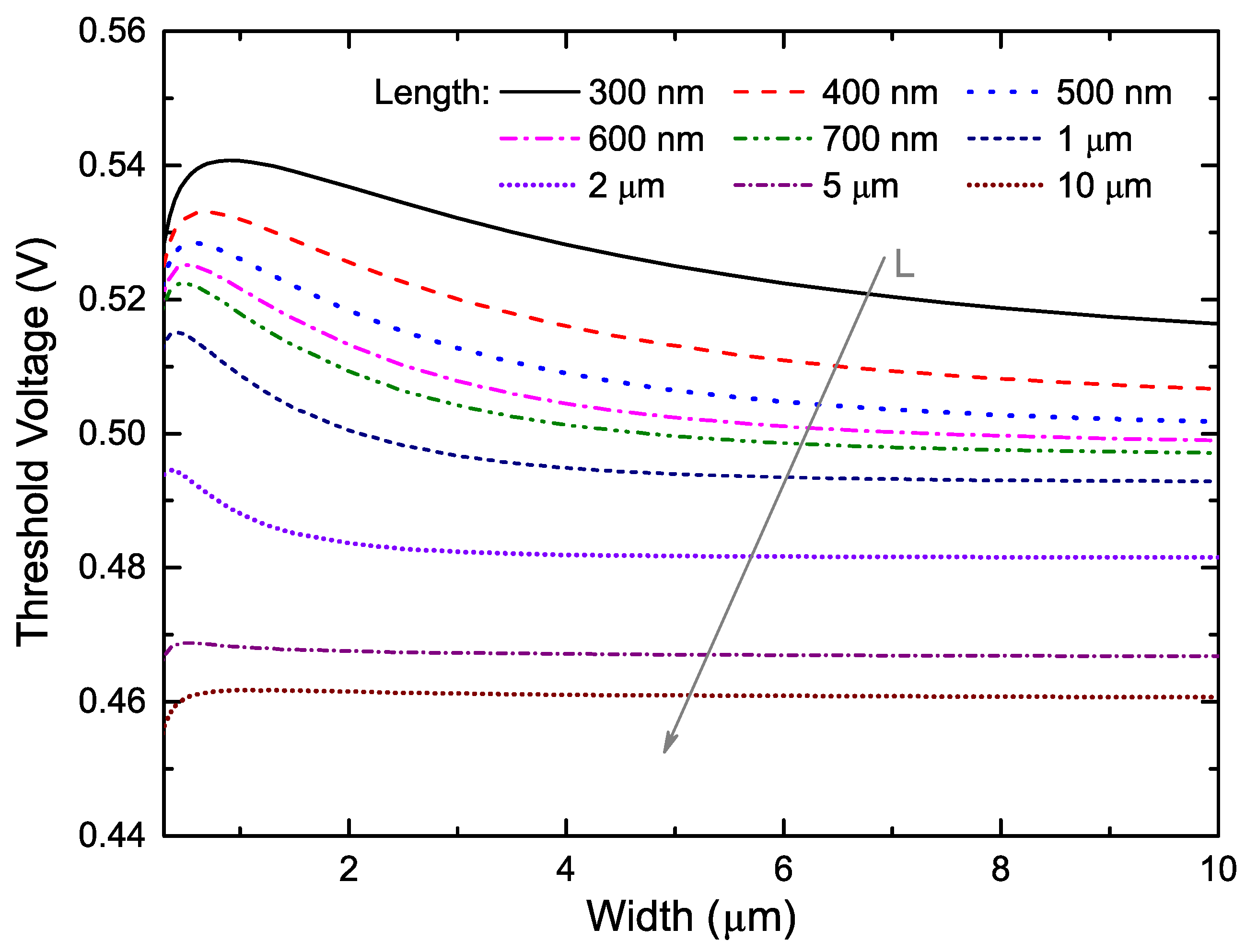
2.2. Proposed Temperature Compensation

In the following, the temperature analysis of the circuit of Figure 1 is expanded to the case where V t h 3 V t h 4 and V t h 5 V t h 6 . The Enz–Krummenacher–Vittoz (EKV) model [47,48] is used to model transistor behavior in both the strong-inversion (SI) and the weak-inversion (WI) regions. Assuming forward saturation conditions, we employed the following basic equations:
I D = I S exp | V G B | n | V S B | | V t h | n U T ( WI ) , β 2 n | V G B | n | V S B | | V t h | 2 ( SI ) ,
where n is the subthreshold slope factor, β = μ C o x m W / L , and I S = 2 n μ C o x U T 2 m W / L , with C o x indicating the oxide capacitance per unit area. The use of the absolute values in (1) makes such equations valid to model both NMOS and PMOS. By means of straightforward calculations, hereby omitted for greater conciseness, the following relationship can be found to express current I 1 , flowing in the left circuit branch of Figure 1:
I 1 = β 3 2 n 3 | V t h 3 | | V t h 4 | + V S G 5 V S G 6 h / k 1 2 = β 3 2 n 3 Σ V t h + n 5 U T ln ( k u ) h / k 1 2 ,
Σ V t h = | V t h 5 | | V t h 6 | + | V t h 3 | | V t h 4 | .
In these relationships, only systematic threshold voltage differences due to geometry-dependent effects are taken into account, while random mismatch errors are not included in the analysis. Referring to (2), it is worth noting that, if Σ V t h = 0 , the aforementioned μ U T 2 trend is indeed obtained for I 1 . Conversely, if M 3 and M 4 (and/or M 5 and M 6 ) have unequal threshold voltages, such that Σ V t h is positive and decreasing with temperature, first-order temperature compensation is made possible after optimization of the slope of n 5 U T ln ( k u ) . To generate the required V t h differences, we propose leveraging geometry dependences of V t h , as explained later. However, prior to presenting more detailed theoretical analyses, a qualitative illustration of the proposed temperature compensation is given in Figure 2. Once transistor pairs M 3 - M 4 and/or M 5 - M 6 are sized to achieve positive Σ V t h , the slope of the PTAT term n 5 U T ln ( k u ) can be adjusted by acting on the k or u ratio between the aspect ratios of matched transistors. By reaching an optimal slope value for the overdrive voltage of M 3 , [proportional to V o d 3 = Σ V t h + n 5 U T ln ( k u ) ], the temperature behavior of mobility, appearing within the transconductance factor β 3 in (2), can be compensated, leading to I R E F with first-order temperature compensation.
Moving the discussion to the method used to generate the Σ V t h term, Figure 3 illustrates the variation of | V t h | as a function of W and L for a PMOS transistor of a commercial 0.18 µm CMOS process. The reported trends were obtained by means of Spectre simulations of device models provided by the silicon foundry. After initial non-monotonic behavior around small device dimensions, | V t h | undergoes considerable reduction as both W and L increase, due to the narrow-channel effect (NCE) [49] and the reverse short-channel effect (RSCE) [50]. While many concurrent factors may contribute to determine such trends, which are highly dependent on the specific transistor type and manufacturing process, NCE is generally due to the fact that, as channel width narrows, the depletion region partially extends beyond the gate edges, particularly where the gate crosses the field oxide, increasing the threshold voltage at small W values. On the other hand, the RSCE is a consequence of halo implants, performed in several CMOS processes to counteract the short-channel effect (SCE) [51]. Halo implants create localized increases in dopant concentration near the source and drain regions, causing increased V t h as L decreases [50]. Then, referring to (2)−(3), Σ V t h > 0 may be achieved by designing M 3 (and/or M 5 ) with short and/or narrow channels, while M 4 (and/or M 6 ) should be sized with long and/or wide channels.
Concerning the temperature dependence of Σ V t h , its TC can be expressed as follows:
α Σ V t h = α V t h 5 α V t h 6 + α V t h 3 α V t h 4 ,
where α V t h 3 6 are the TCs of | V t h 3 6 | , according to the following temperature model [45]:
| V t h ( T ) | = | V t h ( T 0 ) | + α V t h ( T T 0 ) .
The threshold voltage of MOS transistors notoriously decreases with temperature ( α V t h < 0 ), due to increased minority carrier concentration at higher temperature, reducing the required gate voltage to invert the channel. Nevertheless, given two transistors M A and M B , designed with short/narrow and long/wide channels, respectively, predicting the sign of α V t h A α V t h B is not straightforward. However, referring specifically to the RSCE, it should be noted that it is a consequence of the average dopant concentration in the channel increasing as L decreases (with small L, the highly doped halo regions play a more significant role). As implied by device physics models [52], higher doping of the channel implies greater V t h sensitivity to temperature, suggesting α V t h to be smaller (more negative) for short-channel devices.
The latter assumption is confirmed by the simulation results of Figure 4: | V t h A | | V t h B | is plotted as a function of temperature in the case where transistor M B is sized with both W and L twice as large as those of M A . For different sizing choices of M A , the temperature trend of the threshold voltage difference remains NTC, with a slope around −0.5 mV/°C.
Resuming the analysis of the CR core of Figure 1, differentiating both terms of (2) with respect to temperature leads to the following result:
1 I 1 I 1 T = 1 T α μ + 2 α Σ V t h T + 2 n 5 U T ln ( k u ) Σ V t h + n 5 U T ln ( k u ) .
In the case where Σ V t h = 0 (i.e., if devices within pairs M 3 , 4 and M 5 , 6 are designed with matched W and L), (6) evidently simplifies into 1 I 1 I 1 T = 2 α μ T . In this case, unless the mobility temperature exponent, α μ , is exactly equal to 2, first-order temperature compensation cannot be performed. On the other hand, by introducing the Σ V t h term with negative TC ( α Σ V t h < 0 ), first-order temperature compensation is made possible. Specifically, the value of Σ V t h should be optimized by imposing proper ratios between the channel widths and lengths of M 4 and M 3 (and/or M 6 and M 5 ), so that the following condition is met at the temperature T 0 , where a zero temperature derivative is desired:
Σ V t h ( T 0 ) = 2 α Σ V t h T 0 α μ + 2 α μ 1 n 5 U T 0 ln ( k u ) .
In this relationship, U T 0 indicates the value assumed by the thermal voltage at temperature T 0 . If (7) holds true, the expression of I 1 can be rearranged into the following:
I 1 ( T ) = I 1 ( T 0 ) T 0 T α μ 1 + α μ 2 T 0 ( T T 0 ) 2 ,
which is a parabolic-like function of temperature, with its minimum point located at T = T 0 .
In future research, the proposed temperature compensation approach might be also extended to emerging non-CMOS technologies, such as Carbon NanoTube Field-Effect Transistors (CNTFETs). Implementing a CR in this technology would be a pivotal addition to recently proposed Operational Transconductance Amplifier (OTA) solutions [53], yielding a compact reference circuit with low quiescent consumption, but careful consideration of CNTFET variability, temperature dependence, and matching properties would be needed.

2.3. Complete Current Reference Design

In Figure 5, the complete architecture of the proposed CR is shown at the transistor level.
In addition to the previously discussed CR core, a feedback branch was included, made up of transistors M 7 9 , to minimize sensitivity to supply voltage variations. An auxiliary start-up circuit is also present, composed of M s 1 4 . Moreover, since specific values of W and L are needed in order to apply the above-discussed temperature compensation, stacked configurations were used to implement M 3 , M 4 , and M 8 , to reduce current consumption down to a few hundred nA without acting on individual channel lengths. Within each stack of transistors, all of the body terminals of individual devices were connected to the source terminal of the upper device, allowing all transistors to share the same N-well. This choice avoids the need for inter-well spacing, leading to smaller area occupation.
Concerning the LS correction, we adopted a technique inspired by [35,36] and adapted to the proposed architecture. In the basic CR version of Figure 1, the V D S differences between transistors M 1 - M 2 and M 3 - M 4 directly follow V d d variations (i.e., Δ V D S 2 , 1 = V D S 2 V D S 1 = V d d V S G 5 V S G 6 V G S 1 ). This may cause relatively large LS due to finite output impedances of the current mirrors. Conversely, in the circuit of Figure 5, the addition of the M 7 9 circuit branch reduces the magnitude of the V d d -to- Δ V D S 2 , 1 sensitivity by a factor roughly equal to the intrinsic gain of M 7 . Intuitively, it can be noted that, if ρ 8 / ρ 3 = ρ 9 / ρ 5 = γ , a linear proportionality relationship exists between the currents flowing in the two considered branches (i.e., I D 8 = γ I D 3 ). Thereafter, if ρ 7 / ρ 2 = γ , transistors M 7 and M 2 result in the same gate-source voltages, forcing V D S 1 = V G S 7 = V G S 2 = V D S 2 . To ensure loop stability, M 2 has to take the role previously played by M 1 as the input device of the n-type current mirror, while M 8 acts as the input device of the p-type current mirror. In addition, to strengthen stability, we applied Miller compensation between the branches M 1 , 4 , 6 and M 7 , 8 , 9 . At start-up, exploiting the pull-up effect from M 8 , 9 , capacitor C C also assists in streamlining the turn-on process of the circuit.
In Table 1, we summarize the device sizes selected to implement the proposed CR.
For greater simplicity, we chose to exploit V t h geometry dependences only in the M 3 , 4 transistor pair, while M 5 and M 6 were sized with equal widths and lengths. The dimension ratios W 4 / W 3 and L 4 / L 3 were chosen based on parametric simulations aimed at TC minimization. For the parameters previously introduced to express ratios between the aspect ratios of different transistors, the following values were selected: k = 1 , h = 2 , u = 3 , and γ = 1 / 4 . The passive devices used for frequency compensation, set equal to C C = 530 fF and R C = 620 kΩ, were implemented as a Metal–Insulator–Metal (MIM) capacitor and a high-resistivity polysilicon resistor, respectively.
The layout view of the proposed CR is shown in Figure 6. It occupies an area of 70 × 45 µm2.

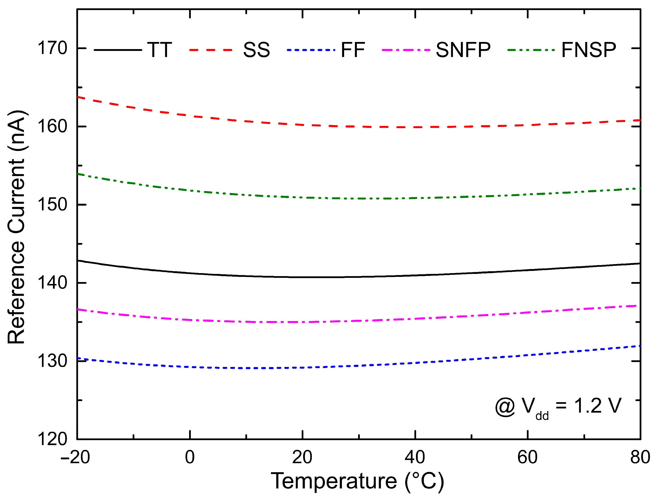
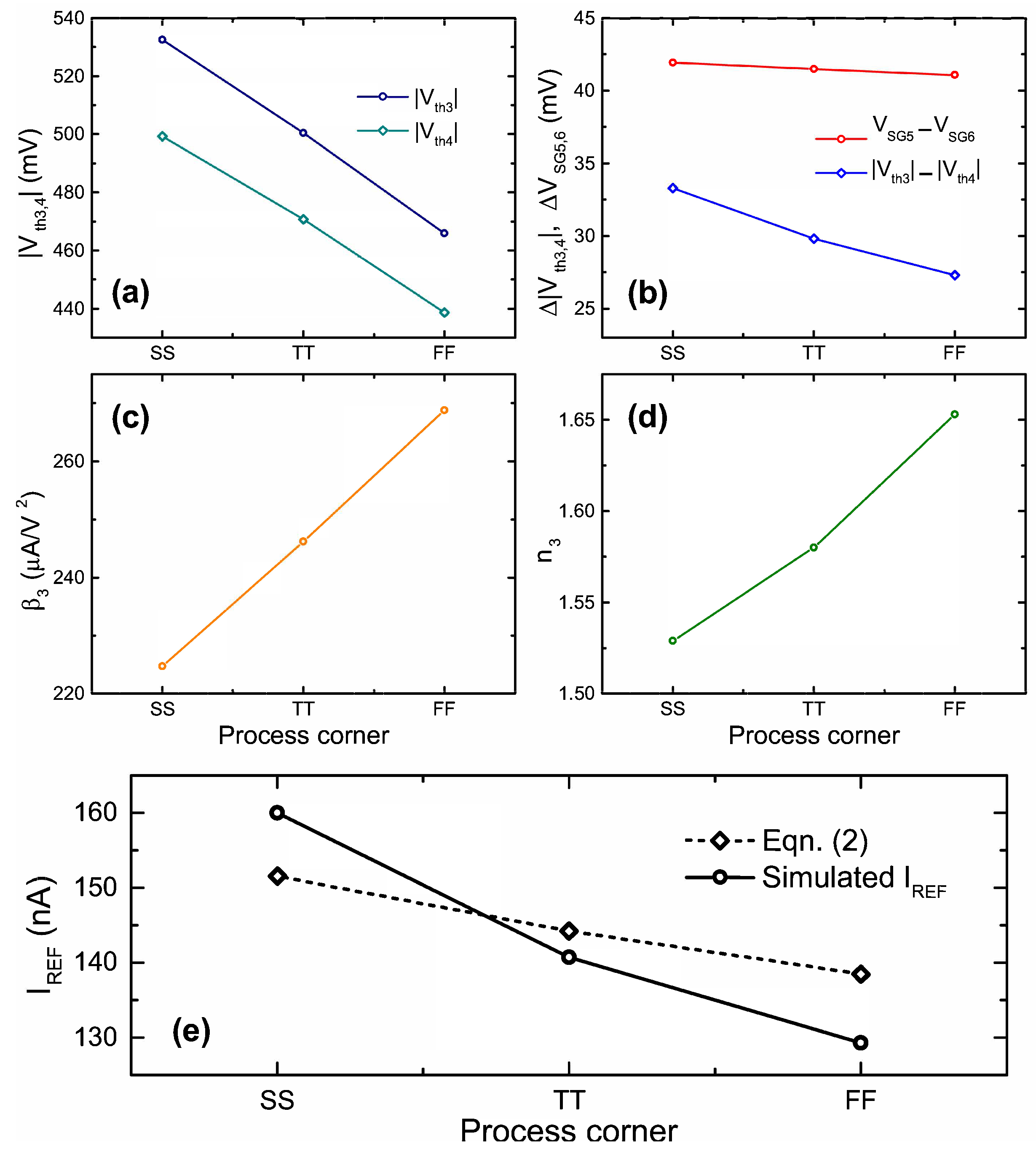
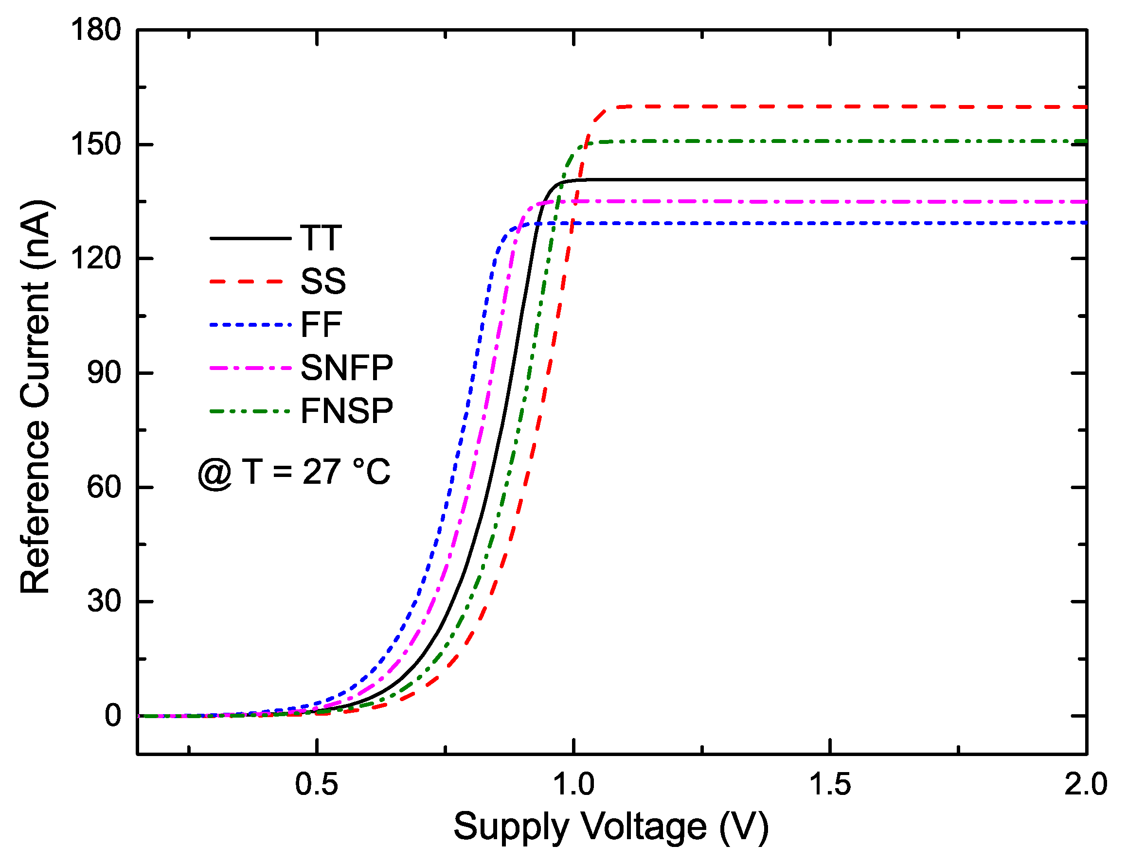
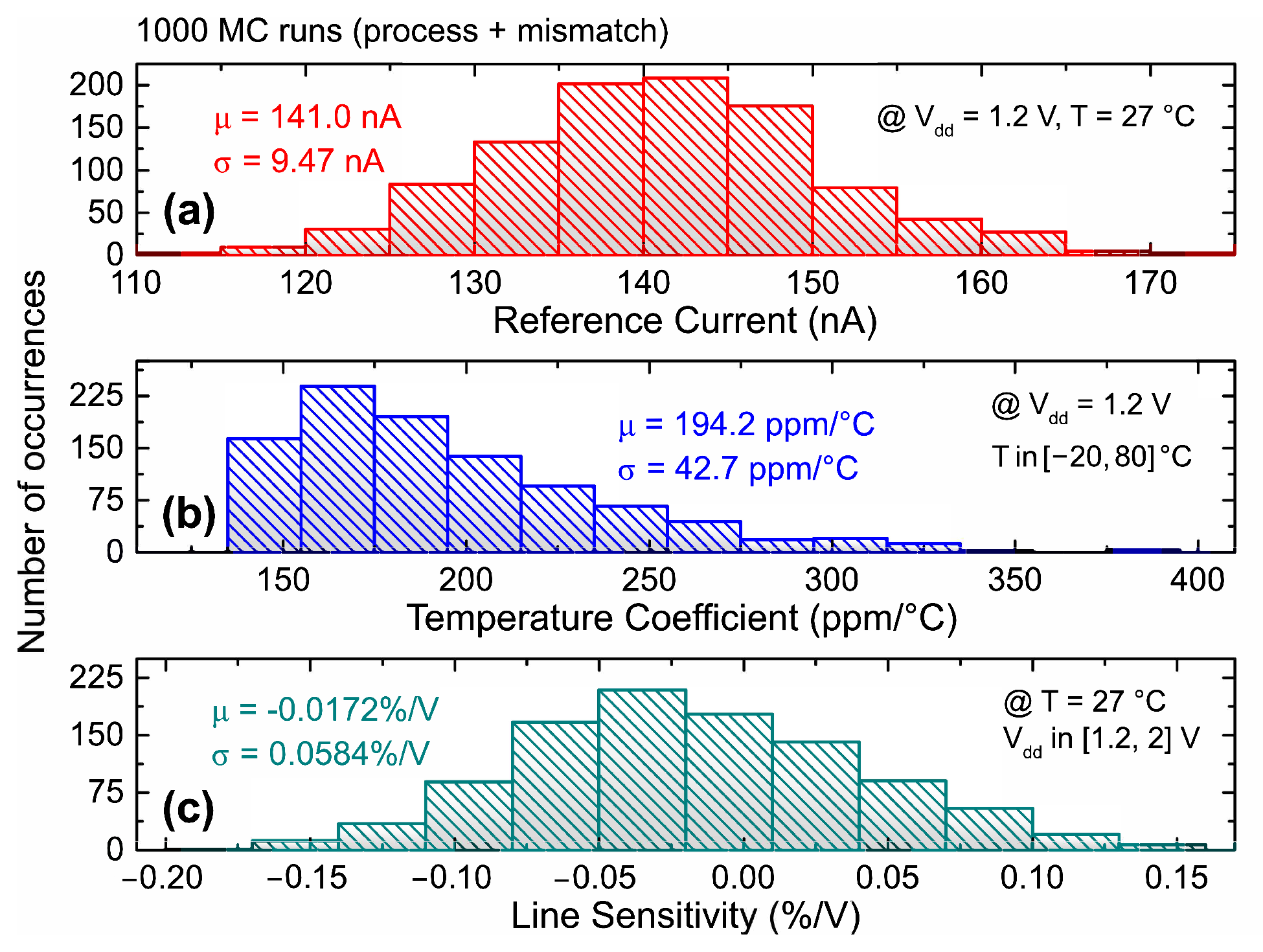
3. Simulation Results

In this section, the results of post-layout electrical simulations are reported to validate the proposed CR. Simulations were executed with the Spectre simulator, using device models of a commercial 0.18 µm CMOS process and models of layout parasitic components obtained from parasitic extraction procedures. Unless otherwise specified, simulations were performed in the typical process corner at room temperature ( T = 27 °C), with the supply voltage set equal to V d d = 1.2 V.
Figure 7 illustrates the temperature behavior of the reference current I R E F (defined as the current flowing through M 1 in Figure 5). Multiple traces are shown, related to the following process corners: Typical (TT), Slow (SS), Fast (FF), Slow-NMOS–Fast-PMOS (SNFP) and Fast-NMOS–Slow-PMOS (FNSP). In the typical corner, I R E F = 140.7 nA is achieved at room temperature, with a total consumption of I s u p = 314.2 nA and TC = 152.8 ppm/°C from −20 °C to 80 °C. Across the other corners, the worst-case TC is equal to 242.2 ppm/°C, obtained in SS conditions.
It is worth noting that the highest reference current value is achieved in the SS corner, while the FF corner features the lowest I R E F . This behavior seemingly contradicts the practical results achieved in other types of CRs [37,43], which show highest I R E F in the FF corner due to decreased threshold voltage and increased mobility. Such behaviors of V t h and μ also exist in the CMOS process employed in this work; however, the proposed CR operates such that the overdrive voltage of transistors M 3 and M 4 also changes across process corners, contributing to the overall process corner variations of I R E F . In Figure 8a–d, we illustrate the process corner variations of all the device parameters appearing in the first formulation of (2), namely | V t h 3 | | V t h 4 | , V S G 5 V S G 6 , β 3 , and n 3 . Furthermore, in Figure 8e, the I R E F values obtained from electrical simulations are compared with those predicted by computing (2) using the simulated device parameters. A Complementary To Fast-skewed Process corner (CTFP) behavior is confirmed for I R E F , evidently determined by the reduction in | V t h 3 | | V t h 4 | and the increase in n 3 in the FF corner. The small discrepancies between the two traces of Figure 8e are arguably due to second-order effects not taken into account in the simplified analytical model leading to (2) (e.g., use of an approximated form of the EKV model, V D S effects, and modeling the stacks of N devices, used to implement M 3 and M 4 , as single devices with length equal to N L 0 , where L 0 is the length of the individual stacked devices). The CTFP behavior of I R E F has also been assessed in [38], even though for a different CR topology.
Figure 9 shows the reference current as a function of the supply voltage, again plotted for various process corners. Based on such results, the minimum supply voltage is assumed to be equal to V d d , m i n = 1.2 V. For V d d [ 1.2 V , 2 V ] , the LS is equal to −0.0251%/V in the typical corner, while a worst-case value of 0.171%/V is obtained in the FF corner.
Table 2 summarizes the main CR performances evaluated across process corners.
To characterize the sensitivity of the proposed circuit to random process variations, sets of 1000 Monte Carlo runs were executed, employing the statistical model files provided by the silicon foundry to simulate both global process variations and local mismatch errors. Figure 10 shows the process spread of I R E F , TC, and LS. I R E F has a relative standard deviation of 6.7%. The average TC value is equal to 194.2 ppm/°C, while its 95% quantile is equal to 291.5 ppm/°C. As for the LS, an average value and a standard deviation equal to −0.0172%/V and 0.0584%/V, respectively, were assessed.
In Figure 11, the Power-Supply Rejection Ratio (PSRR) is shown as a function of frequency. This quantity is herein defined as the rejection ratio of V d d variations towards I R E F , assuming the dimension of a conductance. It is equal to −199.3 dB Ω 1 at 1 Hz, −170.2 dB Ω 1 at 1 kHz, and −125.2 dB Ω 1 at 1 MHz.
The noise current spectrum is illustrated in Figure 12, evaluated at the drain terminal of M 1 . At room temperature, the broad-band noise floor and the flicker corner frequency are equal to 1.1 pA / Hz and 410 Hz, respectively. The integrated noise is equal to 43.31 pARMS from 0.1 Hz to 10 Hz and 1.22 nARMS from 0.1 Hz to 100 MHz.

4. Conclusions

In this work, we presented a CMOS-only CR based on a novel temperature compensation approach, exploiting geometry-dependent threshold voltage effects. We demonstrated how the temperature behavior of BM-CRs can be beneficially shaped by introducing width- and/or length-dependent threshold voltage differences within specific pairs of transistors. Accurate post-layout simulations were executed to validate the proposed design, including process corner analyses and statistical Monte Carlo simulations.
In Table 3, the attained performances are compared to prior art. In addition to the main circuit performances, we also indicated the specific design methods employed in the selected designs, the presence/absence of other types of devices besides MOS transistors and the use of trimming. Furthermore, a Figure of Merit (FoM) is also introduced, to allow more immediate comparisons among various works. As of today, in the context of CRs, little emphasis has been devoted to proposing and validating FoMs encompassing the main circuit performances. Among the references considered in this work, FoMs are proposed in [27,31], but such quantities only take into account TC, temperature range, power consumption, and area occupation, while neglecting LS. Nevertheless, depending on the considered application, resilience against supply voltage variations may represent a crucial concern. That is the case, for instance, of electronic devices supplied by energy-harvesters, often including charge-pump-based up-shifting of the supply voltage provided by the harvester [54], at the cost of non-negligible fluctuations being superimposed onto the final V d d level. In such scenarios, minimal LS is indeed required. According to such motivations, we hereby introduce an FoM focusing on supply and temperature immunity, as well as power and area efficiency. Specifically, we employ the FoM previously proposed in [31] with the addition of LS as a multiplying factor, leading to the following definition:
FoM = TC T m a x T m i n · I s u p I R E F · LS · Area .
Designs characterized by lower FoM values deliver better performance in terms of I R E F stability and efficiency.
The LS accomplished by this work is the smallest among the reported references, proving strong effectiveness of the employed LS correction technique. The achieved LS reduction comes at the cost of increased power consumption, due to the additional circuit branch; however, in the presented design, the additional transistors have been sized to limit the efficiency loss to around 12.5%. Acting only in terms of V D S stabilization, the proposed method does not modify the temperature compensation approach with respect to the original six-transistor CR. Among the works operating at similar current levels (hundreds of nA), [37] is the only one achieving an LS of the same order of magnitude as our work. A different BM structure is employed (resistor-based peaking CR, placing the resistor on top of a diode-connected transistor in the non-linear mirror, rather than in series to its source terminal), but the authors of [37] also apply an LS improvement method based on an additional circuit branch introducing negative feedback. On the other hand, [38,39,40,42] attempt to reduce LS by implementing the BM structure using standard cascode current mirrors, while [41] uses a pseudo-cascode current mirror, and [43,44] include mirrors assisted by auxiliary amplifiers for V D S control, but all of these works ultimately achieve LS values higher than 0.3%/V.
The TC obtained in this work is also in line with previously demonstrated CRs designed for similar current ranges. Among such works, refs. [27,37] reported significantly lower TC; however, for the design presented in [37], the area occupation is more than two times higher than in our design, partly due to the use of a resistor in this CR, while the small TC achieved in [27] is traded off with an LS metric about 80 times higher than the result obtained in this work. In future research, the TC of the proposed CR may be further reduced by adding trimming schemes and Segmented Curvature Compensation (SCC) strategies [55,56,57], to apply effective high-order temperature compensations.
Concerning the effects of random process variations, the relatively large standard deviation of I R E F assessed for the proposed CR (indicated in relative terms in Table 3, as σ / μ ) is a consequence of the small area budget (third-smallest area in Table 3) adopted in this work to enhance suitability for low-cost and low-size ICs. In this respect, it is worth noting that [39], reporting a CR designed with an analogous current level and area occupation, and, like our work, without trimming approaches, is characterized by a similar σ / μ value. However, for applications imposing more stringent yield requirements, the proposed CR design can be complemented by various well-established accuracy improvement techniques. In the first place, in system architectures presenting only one CR core, serving all of the other blocks instantiated on-chip, larger area occupation is arguably tolerable, allowing reduction in the variance of mismatch errors. Moreover, layout techniques enhancing symmetry and matching of the three main device pairs ( M 1 - M 2 , M 3 - M 4 and M 5 - M 6 ) can be adopted, including bidimensional common-centroid layouts, minimizing the effects of on-chip gradients on the device parameters. In addition, resilience to both mismatch and gradient errors may be enhanced by implementing Dynamic Element Matching (DEM) strategies [36,56,58,59], allowing the trade off of operating frequency for accuracy, rather than sacrificing area. On the other hand, concerning global process variations, batch-trimming approaches can be implemented (i.e., trimming one chip per fabrication run, to correct I R E F against the occurred process corner, and then apply the same trimming code to all chips). This is commonly performed both in VR- and CR MOSFET-based solutions. In the specific case of the proposed CR, a simple programmable current mirror can be added within an output branch replicating the I R E F current towards the supplied circuits. This type of correction, acting on the value of I R E F , is feasible in the form of one-point calibration (i.e., performed at a single temperature). In addition, TC calibration may also be performed relying on two-point trimming of the multiplicity of M 6 , which affects the slope of the PTAT voltage term n 5 U T ln ( k u ) appearing within square brackets in (2). This would allow the recovery of TC errors possibly occurring in fabricated prototypes, due to either inaccurate modeling of temperature effects in the employed device models, or mismatch errors affecting device geometry. Another promising approach for process corner compensation has been recently proposed in [33,34] for VRs, exploiting geometry-dependent threshold voltage effects to control not only temperature dependence but also sensitivity to global process errors. Adapting this approach to BM-CRs, such as the herein proposed circuit, entails interesting perspectives for future research.
Noise performances have been often omitted in previous articles on CRs, hindering the possibility of a clear and extensive overview. Compared to the other works offering noise characterizations, this work achieves RMS noise of the same order of magnitude. Due to the small area of our design and the absence of dynamic noise compensation techniques, such as DEM or chopping, flicker noise is arguably more dominant compared to other published CRs. In future studies, compensation techniques tackling both mismatch and noise might be developed. Furthermore, for the specific case of noise, current-mode low-pass filtering, such as the approach recently presented in [60], might also be promising.
Finally, in terms of the proposed FoM, our work achieves the second-best value among the works compared in Table 3, smaller by about an order of magnitude or more, compared to the other references except [37]. The FoM value achieved by this work is mainly determined by the remarkably low LS and area results, even lower than those reported in [37], which features the best FoM within Table 3.
In conclusion, the reported findings validate the proposed CR architecture as an effective solution to achieve enhanced robustness against supply noise and temperature variations under strict power and area constraints. Thereafter, the proposed solution appears as a good candidate for the integration of CRs within versatile low-cost and low-power ICs for IoT and smart sensing applications.

Author Contributions

Conceptualization, F.G.; methodology, F.G. and P.B.; software, A.R., M.P. and P.B.; validation, F.G., A.R., M.P. and P.B.; formal analysis, F.G.; investigation, F.G.; resources, A.R., M.P. and P.B.; data curation, F.G.; writing—original draft preparation, F.G.; writing—review and editing, F.G. and P.B.; visualization, F.G. and A.R.; supervision, P.B.; project administration, M.P. and P.B.; funding acquisition, M.P. and P.B. All authors have read and agreed to the published version of the manuscript.

Funding

This work was supported in part by the European Innovation Council (EIC) through the Project “Green valorization of CO2 and Nitrogen compounds for making fertilizers (CONFETI)” (grant agreement ID: 101115182).

Data Availability Statement

The original contributions presented in this study are included in the article. Further inquiries can be directed to the corresponding authors.

Conflicts of Interest

The authors declare no conflicts of interest.

References

  1. Rezaeiyan, Y.; Kooliv, Y.; Zamani, M.; Shoaei, O.; Akbari, M.; Moradi, F.; Tang, K.T. A 4.5 µW Miniaturized 3-Channel Wireless Intra-Cardiac Acquisition System. IEEE Trans. Biomed. Circuits Syst. 2023, 17, 1097–1110. [Google Scholar] [CrossRef] [PubMed]
  2. Vohra, J.; Gupta, A.; Alioto, M. Imager with In-Sensor Event Detection and Morphological Transformations with 2.9pJ/pixel × frame Object Segmentation FOM for Always-On Surveillance in 40 nm. In Proceedings of the 2024 IEEE International Solid-State Circuits Conference (ISSCC), San Francisco, CA, USA, 18–22 February 2024; pp. 104–106. [Google Scholar] [CrossRef]
  3. Zamani, M.; Rezaeiyan, Y.; Shoaei, O.; Serdijn, W.A. A 1.55 µW Bio-Impedance Measurement System for Implantable Cardiac Pacemakers in 0.18 µm CMOS. IEEE Trans. Biomed. Circuits Syst. 2018, 12, 211–221. [Google Scholar] [CrossRef] [PubMed]
  4. Sheeraz, M.; Aslam, A.R.; Drakakis, E.M.; Heidari, H.; Altaf, M.A.B.; Saadeh, W. A Closed-Loop Ear-Worn Wearable EEG System with Real-Time Passive Electrode Skin Impedance Measurement for Early Autism Detection. Sensors 2024, 24, 7489. [Google Scholar] [CrossRef] [PubMed]
  5. Bijak, J.; Trawiński, T.; Szczygieł, M.; Kowalik, Z. Modelling and Investigation of Energy Harvesting System Utilizing Magnetically Levitated Permanent Magnet. Sensors 2022, 22, 6384. [Google Scholar] [CrossRef]
  6. Yalagala, B.P.; Zhang, J.; Das, R.; Heidari, H. Advancements in Energy Harvesting for Implantable Cardiovascular Devices. In Wireless Power Technologies for Biomedical Devices. Analog Circuits and Signal Processing; Springer: Cham, Switzerland, 2025. [Google Scholar] [CrossRef]
  7. Alioto, M. Enabling the Internet of Things: From Integrated Circuits to Integrated Systems; Springer: New York, NY, USA, 2017. [Google Scholar] [CrossRef]
  8. Shaikh, F.K.; Zeadally, S. Energy harvesting in wireless sensor networks: A comprehensive review. Renew. Sustain. Energy Rev. 2016, 55, 1041–1054. [Google Scholar] [CrossRef]
  9. Pullela, A.; Ali, A.; Jain, A.; Lee, I.; Abbas, Z. A 156pW Gate-Leakage Based Voltage/Current Reference for Low-Power IoT Systems. In Proceedings of the ISCAS 2022—IEEE International Symposium on Circuits and Systems, Austin, TX, USA, 27 May 2022–1 June 2022; pp. 1923–1927. [Google Scholar] [CrossRef]
  10. Catania, A.; Gagliardi, F.; Piotto, M.; Bruschi, P.; Dei, M. Ultralow-Power Inverter-Based Delta-Sigma Modulator for Wearable Applications. IEEE Access 2024, 12, 80009–80019. [Google Scholar] [CrossRef]
  11. Privitera, M.; Ballo, A.; Grasso, A.D.; Alioto, M. A 15-nA quiescent current capacitor-less LDO for sub-1V µW-powered fully-harvested systems. In Proceedings of the 2024 IEEE International Symposium on Circuits and Systems (ISCAS), Singapore, 19–22 May 2024; pp. 1–5. [Google Scholar] [CrossRef]
  12. Privitera, M.; Grasso, A.D.; Ballo, A.; Alioto, M. 0.6-V, µW-Power Four-Stage OTA With Minimal Components, and 100× Load Range. IEEE Solid-State Circuits Lett. 2024, 7, 311–314. [Google Scholar] [CrossRef]
  13. Sala, R.D.; Centurelli, F.; Scotti, G. A Novel Technique to Design Ultra-Low Voltage and Ultra-Low Power Inverter-Based OTAs. In Proceedings of the 2024 19th Conference on Ph.D Research in Microelectronics and Electronics (PRIME), Larnaca, Cyprus, 9–12 June 2024; pp. 1–4. [Google Scholar] [CrossRef]
  14. Najafizadeh, L. Reference circuits for emerging applications-from extreme environment electronics to internet of things. In Proceedings of the MWSCAS 2017—IEEE 60th International Midwest Symposium on Circuits and Systems, Boston, MA, USA, 6–9 August 2017; pp. 1304–1307. [Google Scholar] [CrossRef]
  15. Moisello, E.; Bonizzoni, E.; Malcovati, P. A 0.756-ppm/°C Time-Domain-Based Curvature-Compensated Bandgap Reference. In Proceedings of the 2023 IEEE International Symposium on Circuits and Systems (ISCAS), Monterey, CA, USA, 21–25 May 2023; pp. 1–5. [Google Scholar] [CrossRef]
  16. Moisello, E.; Bonizzoni, E.; Malcovati, P. MOSFET-Based Voltage Reference Circuits in the Last Decade: A Review. Micromachines 2024, 15, 1504. [Google Scholar] [CrossRef]
  17. Fassio, L.; Hanh, H.H.; Alioto, M. Event-Driven Voltage Reference with Bandgap-Class Temperature Coefficient Across-Corner with 100-pW Power at 0.8 V. In Proceedings of the 2024 IEEE European Solid-State Electronics Research Conference (ESSERC), Bruges, Belgium, 9–12 September 2024; pp. 273–276. [Google Scholar] [CrossRef]
  18. Gagliardi, F.; Ria, A.; Manfredini, G.; Piotto, M.; Bruschi, P. A Triode-Compensated CMOS Bandgap Core for Sub-250 mV Supply Voltages. In Proceedings of the 2022 17th Conference on Ph.D Research in Microelectronics and Electronics (PRIME), Villasimius, Italy, 12–15 June 2022; pp. 85–88. [Google Scholar] [CrossRef]
  19. Gagliardi, F.; Bruschi, P.; Piotto, M.; Sakouhi, S.; Dei, M. Single-Branch NMOS-Only Self-Cascoded Voltage Reference Operating down to 0.28-V Supply. In Proceedings of the 2025 23rd IEEE International NEWCAS Conference (NEWCAS), Paris, France, 22–25 June 2025. [Google Scholar]
  20. Gagliardi, F.; Bruschi, P.; Piotto, M.; Sakouhi, S.; Dei, M. A Multi-Self-Cascoded Voltage Reference with 2.73-ppm/V Line Sensitivity and 20.1-ppm/°C Temperature Coefficient at 0.45-V Supply. In Proceedings of the 2025 68th IEEE International Midwest Symposium on Circuits and Systems (MWSCAS), Lansing, MI, USA, 10–13 August 2025. [Google Scholar]
  21. Wikner, J.J.; Tan, N. Modeling of CMOS digital-to-analog converters for telecommunication. IEEE Trans. Circuits Syst. II Analog. Digit. Signal Process. 1999, 46, 489–499. [Google Scholar] [CrossRef]
  22. Huang, J.; Zhou, T.; Wang, C.; Gu, Z.; Li, Y.; Liu, Y. Design of a High Linearity Sinusoidal Current Generator Using Shifting Current Mirror Architecture. IEEE Trans. Instrum. Meas. 2022, 71, 4008905. [Google Scholar] [CrossRef]
  23. Lee, S.; Sánchez-Sinencio, E. Current Reference Circuits: A Tutorial. IEEE Trans. Circuits Syst. II Express Briefs 2021, 68, 830–836. [Google Scholar] [CrossRef]
  24. Yang, W.-B.; Huang, Z.-Y.; Cheng, C.-T.; Lo, Y.-L. Temperature insensitive current reference for the 6.27 MHz oscillator. In Proceedings of the 2011 International Symposium on Integrated Circuits, Singapore, 12–14 December 2011; pp. 559–562. [Google Scholar] [CrossRef]
  25. Sebastiano, F.; Breems, L.J.; Makinwa, K.A.A.; Drago, S.; Leenaerts, D.M.W.; Nauta, B. A Low-Voltage Mobility-Based Frequency Reference for Crystal-Less ULP Radios. IEEE J. Solid-State Circuits 2009, 44, 2002–2009. [Google Scholar] [CrossRef]
  26. Gagliardi, F.; Catania, A.; Ria, A.; Bruschi, P.; Piotto, M. A Compact All-MOSFETs PVT-compensated Current Reference with Untrimmed 0.88%-(σ/μ). In Proceedings of the PRIME 2023—18th International Conference on Ph.D Research in Microelectronics and Electronics, Valencia, Spain, 18–21 June 2023; pp. 61–64. [Google Scholar] [CrossRef]
  27. Mohamed, A.R.; Chen, M.; Wang, G. Untrimmed CMOS Nano-Ampere Current Reference with Curvature-Compensation Scheme. In Proceedings of the ISCAS 2019—IEEE International Symposium on Circuits and Systems, Sapporo, Japan, 26–29 May 2019; pp. 1–4. [Google Scholar] [CrossRef]
  28. Shima, T. Temperature insensitive current reference circuit using standard CMOS devices. In Proceedings of the 2007 50th Midwest Symposium on Circuits and Systems, Montreal, QC, Canada, 5–8 August 2007; pp. 181–184. [Google Scholar] [CrossRef]
  29. Rodovalho, L.H.; Toledo, P.; Bampi, S. A 0.6 V Current Reference Based on the MOSFET Forward-Body-Biased ZTC Condition. In Proceedings of the 2019 26th IEEE International Conference on Electronics, Circuits and Systems (ICECS), Genoa, Italy, 27–29 November 2019; pp. 290–293. [Google Scholar] [CrossRef]
  30. Gagliardi, F.; Nannipieri, I.; Scognamiglio, M.; Contardi, S.; Ria, A. A PVT-Robust Beta-Multiplier Current Reference with Body-Effect-Based Temperature Dependency Modulation. In Proceedings of the PRIME 2024—19th International Conference on Ph.D Research in Microelectronics and Electronics, Larnaca, Cyprus, 9–12 June 2024; pp. 1–4. [Google Scholar] [CrossRef]
  31. Lefebvre, M.; Bol, D. A nA-Range Area-Efficient Sub-100-ppm/°C Peaking Current Reference Using Forward Body Biasing in 0.11-µm Bulk and 22-nm FD-SOI. IEEE J. Solid-State Circuits 2025, 60, 579–592. [Google Scholar] [CrossRef]
  32. Amaravati, A.; Dave, M.; Baghini, M.S.; Sharma, D.K. 800-nA Process-and-Voltage-Invariant 106-dB PSRR PTAT Current Reference. IEEE Trans. Circuits Syst. II Express Briefs 2013, 60, 577–581. [Google Scholar] [CrossRef]
  33. Ji, Y.; Lee, J.; Kim, B.; Park, H.-J.; Sim, J.-Y. A 192-pW Voltage Reference Generating Bandgap-Vth With Process and Temperature Dependence Compensation. IEEE J. Solid-State Circuits 2019, 54, 3281–3291. [Google Scholar] [CrossRef]
  34. Wang, J.; He, J.; Law, M.-K.; Wang, X.; Liang, F.; Cheng, L. A 76.9 ppm/K Nano-Watt PVT-Insensitive CMOS Voltage Reference Operating From 4 to 300 K for Integrated Cryogenic Quantum Interface. IEEE J. Solid-State Circuits 2025. early access. [Google Scholar] [CrossRef]
  35. Van Staveren, J.; Almudever, C.G.; Scappucci, G.; Veldhorst, M.; Babaie, M.; Charbon, E.; Sebastiano, F. Voltage References for the Ultra-Wide Temperature Range from 4.2K to 300K in 40-nm CMOS. In Proceedings of the ESSCIRC 2019—IEEE 45th European Solid State Circuits Conference, Cracow, Poland, 23–26 September 2019; pp. 37–40. [Google Scholar] [CrossRef]
  36. Van Staveren, J.; Padalia, P.M.; Charbon, E.; Almudever, C.G.; Scappucci, G.; Babaie, M. Cryo-CMOS Voltage References for the Ultrawide Temperature Range From 300 K Down to 4.2 K. IEEE J. Solid-State Circuits 2024, 59, 2884–2894. [Google Scholar] [CrossRef]
  37. Hu, J.; Lu, C.; Xu, H.; Wang, J.; Liang, K.; Li, G. A novel precision CMOS current reference for IoT systems. AEÜ—Int. J. Electron. Commun. 2021, 130, 153577. [Google Scholar] [CrossRef]
  38. Azcona, C.; Calvo, B.; Celma, S.; Medrano, N.; Sanz, M.T. Precision CMOS current reference with process and temperature compensation. In Proceedings of the ISCAS 2014—IEEE International Symposium on Circuits and Systems, Melbourne, VIC, Australia, 1–5 June 2014; pp. 910–913. [Google Scholar] [CrossRef]
  39. Chouhan, S.S.; Halonen, K. A 0.67-µW 177-ppm/°C All-MOS Current Reference Circuit in a 0.18-µm CMOS Technology. IEEE Trans. Circuits Syst. II Express Briefs 2016, 63, 723–727. [Google Scholar] [CrossRef]
  40. Lee, S.; Heinrich-Barna, S.; Noh, K.; Kunz, K.; Sánchez-Sinencio, E. A 1-nA 4.5-nW 289-ppm/°C Current Reference Using Automatic Calibration. IEEE J. Solid-State Circuits 2020, 55, 2498–2512. [Google Scholar] [CrossRef]
  41. Huang, W.; Liu, L.; Zhu, Z. A Sub-200nW All-in-One Bandgap Voltage and Current Reference Without Amplifiers. IEEE Trans. Circuits Syst. II Express Briefs 2021, 68, 121–125. [Google Scholar] [CrossRef]
  42. Veit, D.; Oehm, J. A Current Reference With Multiple Nonlinear Current Mirrors to Reduce Noise, Mismatch, and Impact of Supply Voltage Variation. IEEE Trans. Circuits Syst. II Express Briefs 2023, 70, 1729–1733. [Google Scholar] [CrossRef]
  43. Huang, Q.; Zhan, C.; Wang, L.; Li, Z.; Pan, Q. A −40 °C to 120 °C, 169 ppm/°C Nano-Ampere CMOS Current Reference. IEEE Trans. Circuits Syst. II Express Briefs 2020, 67, 1494–1498. [Google Scholar] [CrossRef]
  44. Ballo, A.; Grasso, A.D.; Privitera, M. A 28-nm, 0.5-V, 78.5-nA Switched Capacitor Current Reference with Active Trimming for sub-1V Implantable Medical Devices. In Proceedings of the 2023 IEEE International Symposium on Circuits and Systems (ISCAS), Monterey, CA, USA, 21–25 May 2023; pp. 1–5. [Google Scholar] [CrossRef]
  45. Filanovsky, I.M.; Allam, A. Mutual Compensation of Mobility and Threshold Voltage Temperature Effects with Applications in CMOS Circuits. IEEE Trans. Circuits Syst. I Fundam. Theory Appl. 2001, 48, 876–884. [Google Scholar] [CrossRef]
  46. Zhang, J.; Wang, Z.; Wang, R.; Sun, Z.; Huang, R. Body Bias Dependence of Bias Temperature Instability (BTI) in Bulk FinFET Technology. Energy Environ. Mater. 2021, 5, 1200–1203. [Google Scholar] [CrossRef]
  47. Enz, C.C.; Krummenacher, F.; Vittoz, E.A. An analytical MOS transistor model valid in all regions of operation and dedicated to low-voltage and low-current applications. Analog. Integr. Circuits Signal Process. 1995, 8, 83–114. [Google Scholar] [CrossRef]
  48. Dei, M. Heuristic Enz–Krummenacher–Vittoz (EKV) Model Fitting for Low-Power Integrated Circuit Design: An Open-Source Implementation. Electronics 2025, 6, 1162. [Google Scholar] [CrossRef]
  49. Kroell, K.E.; Ackermann, G.K. Threshold voltage of narrow channel field effect transistors. Solid-State Electron. 1976, 19, 77–81. [Google Scholar] [CrossRef]
  50. Kim, T.-H.; Eom, H.; Keane, J.; Kim, C. Utilizing reverse short channel effect for optimal subthreshold circuit design. In Proceedings of the ISLPED 2006—International Symposium on Low Power Electronics and Design, Tegernsee, Germany, 4–6 October 2006; pp. 127–130. [Google Scholar] [CrossRef]
  51. Khanna, V.K. Short-Channel Effects in MOSFETs. In NanoScience and Technology—Integrated Nanoelectronics; Springer: New Delhi, India, 2016. [Google Scholar] [CrossRef]
  52. Sze, S.M.; Li, Y.; Ng, K.K. Physics of Semiconductor Devices, 4th ed.; Wiley: Hoboken, NJ, USA, 2021. [Google Scholar]
  53. Jooq, M.K.Q.; Bozorgmehr, A.; Mirzakuchaki, S. An ultra-miniature broadband operational transconductance amplifier utilizing 10 nm wrap-gate CNTFET technology. Analog. Integr. Circuits Signal Process. 2021, 107, 423–434. [Google Scholar] [CrossRef]
  54. Ballo, A.; Grasso, A.D.; Palumbo, G. Charge Pump Improvement for Energy Harvesting Applications by Node Pre-Charging. IEEE Trans. Circuits Syst. II Express Briefs 2020, 67, 3312–3316. [Google Scholar] [CrossRef]
  55. Gagliardi, F.; Ria, A.; Piotto, M.; Bruschi, P. A 114 ppm/°C-TC 0.78%-(σ/μ) Current Reference with Minimum-Current-Search Calibration. IEEE Trans. Circuits Syst. II Express Briefs 2024, 71, 1561–1565. [Google Scholar] [CrossRef]
  56. Park, P.; Lee, J.; Cho, S. A PVT-Insensitive Sub-Ranging Current Reference Achieving 11.4-ppm/°C From −20 °C to 125 °C. IEEE J. Solid-State Circuits 2024, 59, 4057–4067. [Google Scholar] [CrossRef]
  57. Gagliardi, F.; Scognamiglio, M.; Ria, A.; Piotto, M.; Bruschi, P. All-MOSFETs Current Reference Featuring High-Order Segmented Curvature Compensation. In Proceedings of the ICECS 2024—31st IEEE International Conference on Electronics Circuits and Systems, Nancy, France, 18–20 November 2024; pp. 1–4. [Google Scholar] [CrossRef]
  58. Wang, J.; Goh, W.L. A 12.4-kHz on-chip RC oscillator with comparator offset cancellation for PVT variation tolerance. In Proceedings of the 2016 International Symposium on Integrated Circuits (ISIC), Singapore, 12–14 December 2016; pp. 1–4. [Google Scholar] [CrossRef]
  59. Gagliardi, F.; Dei, M. Accuracy Enhancement of Resistor-String Digital-to-Analog Converters through Averaging Dynamic Element Matching. In Proceedings of the 2025 IEEE 28th International Symposium on Design and Diagnostics of Electronic Circuits and Systems (DDECS), Lyon, France, 5–7 May 2025; pp. 74–79. [Google Scholar] [CrossRef]
  60. Jiang, K.; Ji, Y.; Kosunen, M.; Kim, K. A 2.3nA-to-205nA Clock-Tunable Dynamic Current Reference with a Built-In 2nd-Order Current-Mode Low-Pass Filter and Coarse-Fine Regulation. In Proceedings of the 2025 23rd IEEE International NEWCAS Conference (NEWCAS), Paris, France, 22–25 June 2025. [Google Scholar]
Figure 1. Core circuit of the proposed current reference. Transistor parameters are annotated as W (channel width), L (channel length), m (multiplicity factor), and ρ (aspect ratio).
Electronics 14 02698 g001
Figure 2. Qualitative illustration of the employed temperature compensation principle, based on (2).
Electronics 14 02698 g002
Figure 3. Threshold voltage of a PMOS transistor (absolute value) as a function of channel width and length in 0.18 µm CMOS.
Electronics 14 02698 g003
Figure 4. Threshold voltage differences between transistors of different sizes plotted as a function of temperature.
Electronics 14 02698 g004
Figure 5. Schematic view of the proposed current reference, comprising auxiliary circuits for LS correction and start-up assistance.
Electronics 14 02698 g005
Figure 6. Layout view of the proposed current reference. The main circuit components are highlighted by dashed boxes. The compensation capacitor, C C , is placed on top of the CMOS devices, implemented as an MIM capacitor requiring only high metal layers.
Electronics 14 02698 g006
Figure 7. Reference current as a function of temperature.
Electronics 14 02698 g007
Figure 8. Simulated process corner variations: (a) threshold voltages of M 3 and M 4 ; (b) | V t h 3 | | V t h 4 | and V S G 5 V S G 6 ; (c) transconductance factor of M 3 ; (d) subthreshold slope factor of M 3 ; (e) reference current.
Electronics 14 02698 g008
Figure 9. Reference current as a function of the supply voltage.
Electronics 14 02698 g009
Figure 10. Process spread histograms: (a) reference current at room temperature; (b) temperature coefficient; (c) line sensitivity.
Electronics 14 02698 g010
Figure 11. PSRR as a function of frequency.
Electronics 14 02698 g011
Figure 12. Output noise spectrum.
Electronics 14 02698 g012
Table 1. Device sizes.
DeviceWidth (µm)Length (µm)MultiplicityStack
M 1 , M 2 , M 7 5316, 16, 41
M 3 21216
M 4 7.523.76116
M 5 , M 6 , M 9 50.516, 48, 41
M 8 11116
M s 1 , M s 2 , M s 3 10.31, 1, 81
M s 4 0.25512
Table 2. Process corner variations.
TTSSFFSNFPFNSP
I REF (nA)140.7160129.3135.1150.8
I sup (nA)314.2355.8290.2301.9336.2
TC (ppm/°C)152.8242.2219.6157.8208.7
LS (%/V)−0.0251−0.09990.171−0.08010.0375
Table 3. State-of-the-art performance summary.
This
Work
[55]
TCAS-II
2024
 [37]
AEÜ
2021
 [38]
ISCAS
2014
 [27]
ISCAS
2019
 [39]
TCAS-II
2016
 [43]
TCAS-II
2020
 [40]
JSSC
2020
 [41]
TCAS-II
2021
 [31]
JSSC
2024
 [44]
ISCAS
2023
 [42]
TCAS-II
2023
 [56]
JSSC
2024
Techn. (nm)1801801801801801801801801802228180180
Results typeSim.Sim.Sim.Sim.Sim.Meas.Meas.Meas.Meas.Meas.Sim.Meas.Meas.
ApproachBM+
RSCE
BM+
SCC
BMBMBM+
ZTC
BMBMAuto
calib.
BM+
BJT
BMSCBMBJT+
DEM
CMOS onlyYesYesNoNoYesYesYesYesNoNoYesYesNo
TrimmingNoNoNoYesNoNoYesYesYesYesYesNoYes
V dd , min (V)1.21.40.61.21.21.250.81.520.750.521.3
I sup (nA)314.21916345165068437260.8N/A963.810371.1·10343.5·103
I REF (nA)141 *46911550014292.311.61511.578.58.5·10310.3·103
σ / μ (%)6.70.785.460.433.166.124.650.061.150.613.452.130.54
T  range (°C)−20,
80
−20,
80
−20,
120
−40,
120
−40,
85
−40,
85
−40,
120
−20,
80
−45,
125
−40,
85
−20,
60
−35,
125
−20,
125
TC (ppm/°C)194 *114 *15.7 #119 56.4 *177 *169 *289 *89 *89 *115 274011.4
LS (%/V)−0.017 *3.610.046.911.457.51.081.41.760.511.20.30.036
RMS noise (pARMS)43.31
(0.1–10 Hz)
N/A14.7
(0.1–10 Hz)
N/AN/AN/AN/AN/AN/AN/AN/A2750
(10–50 kHz)
38.9
(0.01–10 Hz)
Area (mm2)0.003150.0800.008N/AN/A0.0010.0540.3320.0630.0020.0020.110.08
FoM  µ m 2 ° C 2 V 0.0023113.50.001N/AN/A0.4283.23N/A1.090.01840.045347.30.00956
BM: Beta-Multiplier; RSCE: reverse short-channel effect; SCC: Segmented Curvature Compensation; ZTC: Zero Temperature Coefficient; SC: Switched-Capacitor; DEM: Dynamic Element Matching. * Average value (across Monte Carlo runs including both global variations and mismatch errors, if simulation results are reported, or across multiple chip samples, if measurement results are reported). # Average value across Monte Carlo runs including only mismatch errors. The worst-case reported TC across process corners is 92.1 ppm/°C. TC evaluated in process corner simulations without mismatch errors. TC evaluated in nominal process corner without mismatch errors.
Disclaimer/Publisher’s Note: The statements, opinions and data contained in all publications are solely those of the individual author(s) and contributor(s) and not of MDPI and/or the editor(s). MDPI and/or the editor(s) disclaim responsibility for any injury to people or property resulting from any ideas, methods, instructions or products referred to in the content.

