Article

DROPc-Dynamic Resource Optimization for Convolution Layer

Division of Information and Computing Technology, College of Science and Engineering, Hamad Bin Khalifa University, Doha 34110, Qatar
*
Author to whom correspondence should be addressed.
Electronics 2025, 14(13), 2658; https://doi.org/10.3390/electronics14132658
Submission received: 17 April 2025 / Revised: 13 June 2025 / Accepted: 16 June 2025 / Published: 30 June 2025
(This article belongs to the Special Issue Research on Key Technologies for Hardware Acceleration)

Abstract

The computational complexity of convolutional neural networks (CNNs) becomes challenging for resource-constrained hardware devices. The convolution layer is predominant in the overall CNN architecture, performing the expensive multiplication and accumulation operation. Therefore, designing a hardware-efficient convolution layer will effectively improve the overall performance of a CNN. In this research, we propose a dynamic resource optimization (DROP) approach to improve the power and delay of the convolution layer. The proposed approach controls the computational path in accordance to the interrupts which are dependent on a non-zero-bit pattern. With a single interrupt, our solution provides 42.5% power and 36.7% delay efficiency compared to the standard bit-serial-parallel approach. Moreover, the power consumed by eight parallel functioning blocks is 27.7% less than the traditional bit-parallel approach.

Graphical Abstract

1. Introduction

The recent advancement in deep learning algorithms has initiated a new era of artificial intelligence where ChatGPT and humanoids can serve everyday human needs. Among deep learning algorithms, the convolutional neural network (CNN) is a widely adopted architecture that can be effectively applied for image classification [1,2,3,4], speech recognition [5,6,7,8], object detection [9,10], etc. The overwhelming accuracy of CNNs is acquired at the cost of computational overhead. These computations become more challenging for resource-constrained hardware devices. A general principle to avoid the overhead is to compress the CNN model through pruning, quantization, etc. However, it is possible to improve the overall efficiency of a CNN by targeting the prominent layer of the architecture.
In CNNs, convolutional layers (CLs) play a significant role in building the overall architecture and cause the maximum computational overhead [11]. The number of CLs varies in different CNN architectures. For example, VGG16 has 13 CLs [12], whereas RESNET-18 has 17 CLs [13]. In all Cases, the performance of the CLs can profoundly impact the overall performance of the CNN architecture. Therefore, the parameters of the convolution layers, such as the kernel size [14], strides [15], etc., remain an active research topic in algorithm design. However, the hardware implementation of the CL is more concerned with computational complexity, memory usage, parallelism, etc. It is possible to handle computational complexity by transforming the feature map into a particular domain, as in the case of the Winograd transformation approach [16]. Parallelism in CNNs can be effectively handled using a systolic matrix or a pipelined approach [17,18,19]. These approaches mainly concern the computational speed irrespective of the input pattern.
It has been argued that only 13% of all activation bits in a CNN are non-zero [20]. Therefore, the computation power and delay could be improved by limiting the computation to non-zero bits. Most existing solutions for handling this issue compute the non-zero-bit location before convolution because a straightforward zero-skipping approach may lead to an unacceptable area and power overhead [20]. Details of these approaches are provided in Section 2. This research proposes a dynamic run-time approach to avoid zeros in the activation streams. The proposed approach configures the processing engine according to the input pattern and bypasses the unnecessary computational block accordingly. The maximum speed is obtained when all the activation bits are zero because it only requires a shift operation. With a single interrupt, our solution provides 42.5% power and 36.7% delay efficiency compared to the standard bit-serial-parallel approach. Moreover, eight parallel functioning blocks require 27.7% less power than the traditional bit-parallel approach.
The remainder of this paper is organized as follows. Section 2 and Section 3 describe related work and the proposed approach. The results and comparison with previous approaches are presented in Section 4, followed by a conclusion in Section 5.

2. Related Work

In [21,22], the CL is divided into three operations, i.e., multiplication, addition, and accumulation, with possible pipelining to increase the speed. However, the straightforward implementation of the multiply and accumulate (MAC) operation will create challenges regarding area reuse, processing speed, etc. A pipeline architecture for an online arithmetic-based MAC operation is presented in [19,20,21,22,23]. The solution used redundant bits representation, increasing the computational load, power, and area overhead. Another approach is to transform the input pattern to a unique Winograd domain, which will reduce the computational complexity but requires additional operational overhead as in [16]. In both cases, the MAC operation is independent of the input bit’s pattern due to which they suffer with respect to the area and power overhead.
Instead of transforming the input pattern to Winograd or redundant bit format, it is possible to alter the hardware according to the input bit pattern. Therefore, the DianNao approach is modified in [20] by limiting the execution of the MAC operation to only non-zero bits (or essential bits) of the activation. For example, an activation A = 0010 has only one essential bit, the location of which can be written as 01. Hence, an encoder is used to transform the activation bit into the essential bit location. The weights will be shifted and added according to the list of essential bits per activation. The problem of synchronization occurs when the activations have a different number of essential bits. To avoid such a situation, the processing unit dealing with low-essential bits will remain idle until all the units complete their execution. Another solution for synchronization is to use extra hardware to sort the activation lanes according to the number of essential elements, as reported in [24]. However, sorting the activation lane will not be possible without rearranging the weights because the activation lane and weight pairing can not be changed. Therefore, additional multiplexers are used in the processing unit to manage the weights according to the sorted activation [24]. The reported solution caused extra complexity and hardware overhead, which can be minimized by dividing the activation lanes into groups of 2, 4, or 8. However, this division will raise the same synchronization issue because all the activation lanes in a single window should complete the multiplication and addition before the final accumulation stage. A similar zero-skipping approach is presented in [25], in which a zero vector is computed for each weight and activation. A logical AND operation is performed between the zero vectors to determine the common indices of 1’s in both. However, this impacts the required information because it may reduce the number of essential bits in the activation or weights. The main problem with the zero-skipping approaches lies in the precomputation process of the indices. It is possible to process the indices on a first-come, first-served basis. However, this will double the size of the adder, which, in turn, increases the power overhead.
In [26], the Eyeriss architecture is used to compress the activation data with a run-length compression approach and data gating is used within the processing elements (PEs) to skip unnecessary computations involving zero activations. The approach is further improved in [27], where both the weights and activation bits are transformed in compressed sparse column (CSC) format before processing to improve the speed and efficiency. However, these approaches introduce additional complexity and delay due to the need for address decoding, count tracking, and sequential access logic to identify and align matching non-zero elements. A compressed encoding approach is also utilized in Sparse-CNN (SCNN) [28]. The reported approach performs computations on compressed weights and activations using a Cartesian product-based architecture. However, it incurs overheads due to complex interconnections, address computation, and limited support for non-unit stride convolutions. To address these limitations, a fully sparse tensor accelerator is introduced in [29], that performs efficient inner products using bitmask-based sparse representations. It also proposes a greedy balancing scheme to mitigate load imbalance by grouping filters based on density. However, this rearrangement requires corresponding adjustments to activation mappings, which can be challenging in ASIC designs where activation layouts are typically fixed. Moreover, the output must be reordered to maintain correctness. A similar concept of using sparsity-aware encoding for weights and activations has also been investigated in [30,31,32]. A specialized storage mechanism for encoding the positions of non-zero activations is presented in [33]. However, it still incurs runtime overhead due to the need for position decoding and dynamic data alignment. In [34], a more adaptive compression is introduced using two-symbol Huffman coding to compress both the activations and the weights. A key feature of the design is its dual-mode zero-skipping mechanism which dynamically selects whether to skip activations or weights based on their local sparsity. The decision is facilitated by dedicated flag maps and control logic. The adaptive strategy improves flexibility and performance under varying sparsity conditions. However, it introduces additional control complexity, memory overhead, and hardware resource requirements.

3. Dynamic Resource Optimization Approach for Convolution

The previously presented architectures with and without zero-skipping have their own advantages and disadvantages. Therefore, we propose a partial zero-skipping approach, which has not been reported before to the best of our knowledge. The proposed approach dynamically selects the execution path based on the input pattern to reduce the delay with an adder size equal to the bit width of the weight.

3.1. Design Methodology

The convolution technique requires the multiplication of each activation lane with the corresponding weight value, and their product is added to obtain the final output, as shown in Equation (1), where n is the number of weights or activation lanes. The presence of array multiplication brings complexity along with area, power, and delay overhead for hardware implementation of the bit-parallel convolution approach. Therefore, different solutions have been discussed in the literature with their respective advantages and disadvantages, as explained in Section 2.
C o n v = n = o 8 ( A n × W n )
The generic architecture of the adder tree for convolving a 3 ×3 weight matrix requires four layers of an interconnected CSA, as shown in Figure 1, where the latency of the final output depends on the execution time of each layer. The fundamental principle of our proposed solution is to divide the adder tree into stages where each stage has a controlled circuitry to decide their respective input/output based on the activation bit pattern. In addition to the stage-wise tree architecture, the activation bits are divided into groups to mitigate the unnecessary zero-bit computation. The adder tree is mainly constructed using a carry save adder (CSA), which can add up to three bits in parallel and is independent of the propagated carry. Therefore, the activation bits are divided into groups of three. The reason for dividing the activation bits into a group of three is supported by the fact that the last few layers of the CNN possess 80% zero-activations because of Relu and zero-padding, as argued in [25]. Zero-padding is performed at image boundaries to maintain the feature size. Therefore, a group of three activations will cover the boundaries, especially in the case of a 3 ×3 weight matrix where one or more of the activation groups will become zero because of zero padding, as shown in Figure 2, where the first row of the second frame and last row of the fourth frame are all zeros. This research considers a 3 ×3 weight matrix size with an 8-bit fixed point representation for each weight and activation bit pattern.
Since the weights for each channel in the deep learning algorithm remain the same for the whole image, the activation might change depending on the stride. Therefore, the proposed design used the serial-parallel MAC approach in which the activation bits are taken serially, whereas the weights are used in parallel. Each activation bit starts from the least significant position multiplied with their respective weights using a logical AND operation. The result of each product is added using the proposed adder tree and accumulated based on the activation bit pattern, as shown in Equation (2), where k , l , m indicates the position of weights or activation lanes, while i is equal to the number of bits in the activation lane. The resulting sum is shifted by a single bit before commencing the next bit operation from left to right. The following terminologies are used frequently in this article:
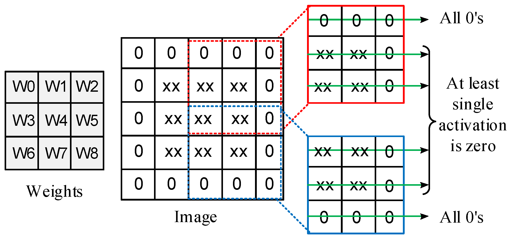
  • Activation vector: Refers to the combination of activation bits from all lanes per cycle. For example, in the case of a 3 × 3 weight matrix, the activation bus consists of nine activation lanes, each having an 8-bit size, and for every cycle, we consider 1 bit from each lane. The single bits from all activation lanes are combined into an activation vector.
  • Activation group or group of activation: Refers to a group of three activation lanes. For example, a 3 × 3 weight matrix will have three groups of activation.
  • Interrupt: Indicates the presence of essential bits in the activation group at a given clock cycle. Each activation group has a dedicated interrupt signal.
C o n v p r o p o s e d = i = o 7 [ k = o 2 ( A k [ i ] × W k ) + l = 3 5 ( A l [ i ] × W l ) + m = 6 8 ) ( A m [ i ] × W m ) > > 1 ]

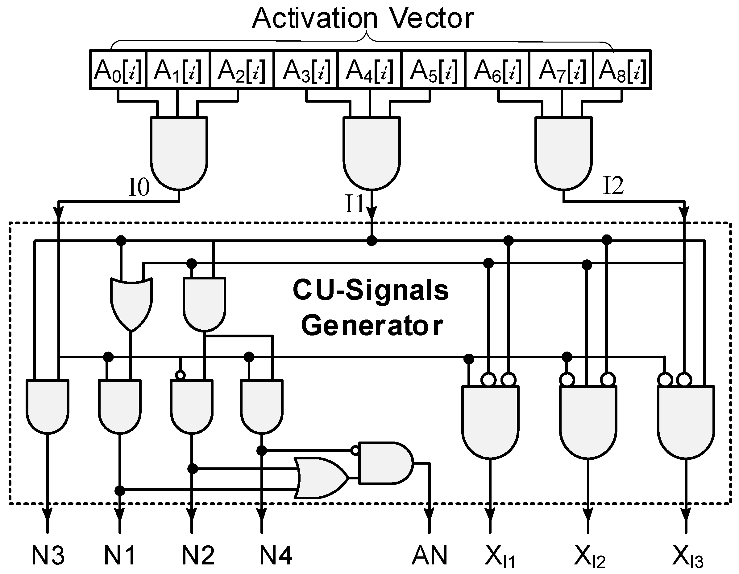
3.2. Architectural Description

In the proposed approach, the adder tree is divided into four stages, with each stage generating outputs for specific activation groups. In addition, each stage, except for the first one, is preceded by a control unit (CU) whose job is to adjust the inputs according to the status of the activation groups, as shown in Figure 3. The design uses an interrupt signal for each activation group to indicate its status. The interrupt signal is computed by dividing the activation vector into three arrays where each array corresponds to an activation group. The logical AND operation for each array will provide the interrupt status for the corresponding activation group at a given clock cycle, as shown in Figure 4. The interrupt signal will be high if the associated array has at least one essential bit. Suppose we have an activation vector of 000001110 at a given clock cycle; the vector will be divided into three arrays such that G0 = 110, G1 = 001, and G2 = 000. Let I0, I1, and I2 be the respective interrupt values for G0, G1, and G2. Then, their values will be I0 = 1, I1 = 1, and I2 = 0, respectively. These interrupts will be used to configure the architecture according to the signals provided by the CU-signals generator shown in Figure 4. A non-zero interrupt mode is used to control the computational path, thereby avoiding the logic inversion required in zero mode. This reduces the complexity and delay overhead caused by additional inverters.
Since the product size is double the size of the multiplicand, a 16-bit register is used to store the results. The output from the final stage is stored in the register’s eight most significant bit locations and will be shifted to the right with the next clock cycle. The final stage takes the partial sum and carry bits from the one of the previous three stages in accordance with the interrupt’s status and then adds them with the eight most significant bits of the sum register. Moreover, the adder size remains 8-bit because of the single-bit shift process at each cycle. Since the CSA can only provide partial sum and carry bits, a carry propagate adder (CPA) is required in the final stage to complete the summation. The selection of the CPA is also critical because this research aims to improve the delay along with the power overhead. In this research, we use a carry prefix-based high-speed and low-power CPA [35]. The reported design is constructed for adding three bits by using a combination of a CSA and CPA. Therefore, it is used in the final stage of the proposed architecture.

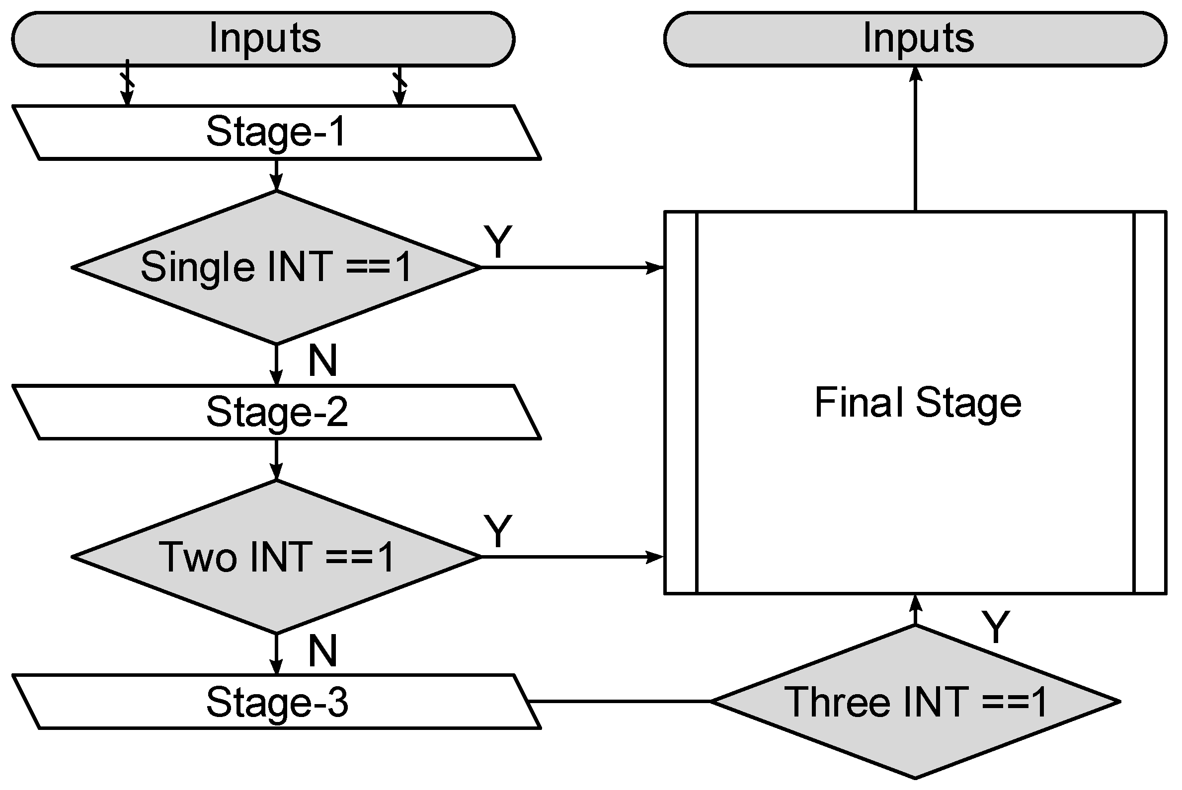
3.3. Operational Behavior

The operational difference between the conventional and the proposed approach is the controlled input for each stage. The control circuitry mainly depends on the interrupts I0, I1, and I2. These interrupts define the hypothetical nodes acting as logical operators to control the proceeding stage’s input pattern. The proposed design uses five such nodes. The first controller is placed before the second stage, which can only be activated if at least two interrupts are high. Therefore, each node value depends on a combination of two or three interrupts, as shown in Figure 4. Moreover, the control unit of Stage 2 (CU-ST2) is designed to ensure that simultaneously active nodes do not conflict in their control of output selection, as shown in Figure 3. In scenarios where two nodes can be active at the same time, as in the case of N1 and N3, they are connected to separate select lines to prevent interference with the same output path. This separation in the control logic guarantees conflict-free operation even when multiple interrupts are active. The node1 (N1) will be high if I0 is high, along with any or both remaining interrupts. In contrast, if I0 is low, while both the remaining interrupts are high, then node2 (N2) will be high. Node3 (N3) depends on I0 and I1, and its value will be high when both are high, as shown in Equation (5). Node4 (N4) is only high if all the interrupts are high, and therefore, it is used to activate the third stage, as shown in Equation (6). An additional node (AN) is required to ensure that any two of the interrupts are at high states because N1 indicates I0 is high along with some other interrupt while N2 covers the case when the other two interrupts are high. However, both N1 and N2 can not be high at the same time as evident from Equations (3) and (4). Moreover, N1 will also be high if all the interrupts are high, as shown in Table 1. Hence, N1 and N2 can not be used to determine that only two interrupts are high. Therefore, an AN node is required with an inverted N4 value to avoid the condition of all interrupt signals being high, as depicted in Equation (7).
N 1 = I 0 ( I 1 + I 2 )
N 2 = I 0 ¯ ( I 1 · I 2 )
N 3 = I 0 · I 1
N 4 = I 0 · I 1 · I 2
A N = N 4 ¯ ( N 1 + N 2 )
The first stage produces a sum and carry bit for each activation group. The output of this stage will be taken to the final stage if only a single interrupt is high; otherwise, the second stage will be invoked for more than one interrupt signal. However, the operation of the second stage depends on the number of interrupt signals. If two interrupts are high, then one of the outputs of this stage will be looped back to it using control circuitry while the other one will be moved to the final stage; otherwise, both will proceed to the third stage, which is responsible for handling the third interrupt. The output of the third stage will only be fed to the final stage, which is responsible for computing and accumulating the final output. Hence, the final stage will receive five possible sums and carry bits as inputs. The first three inputs belong to the first stage, which handles individual interrupts, while the other two are from the second and third stages. The inputs from the last two stages can easily be handled by nodes AN and N4. However, the remaining three from the first stage require additional logic of X I 1 , X I 2 and X I 3 to handle each interrupt individually by keeping the corresponding interrupt signal high while inverting the other two interrupts. For example, if I1 is high, the respective output of X I 1 will allow S1 and C1 to proceed to the final stage. The overall interrupt mechanism for dynamically reconfiguring the computational path is shown in Figure 5.
The output from the final stage is stored in the register’s eight most significant bit locations and will be shifted to the right with the next clock cycle. At the same time, the eight most significant bits are looped back to the final stage to accommodate the summation of the next cycle. If all the interrupts are zero, then the output register will be shifted without computation, and therefore, the maximum clock frequency can be used to reduce the delay of the architecture. However, in case of an interruption, the clock frequency can be controlled using a clock gating approach in which the clock depends on a combinational circuit. Suppose the input clock for the system is connected with the logical AND gate whose inputs are linked to the clock signal and inverted interrupt bit. If the interrupt is high, the clock will remain idle for the system till the interrupt is released. The delay path (DP) for different interrupt conditions is shown in Figure 6a. There are four possibilities of interrupt signals, and each of them is classified as a different case. Case-0 refers to the condition when all the interrupts are low and require only a shift operation, as depicted in Equation (8). Case-1 represents the condition when a single interrupt is high. It only requires the execution of the first stage and final stage. Therefore, its delay can be estimated using Equation (9). The condition of having two active high interrupts is referred to as Case-2, which involves the execution of the first two stages, along with the last stage, as depicted in Equation (10). The last possibility is Case-3, where all interrupts are active high and require the execution of the overall architecture. It is considered to be the worst Case with delay shown in Equation (11). The general operation is shown in Figure 6b for three activation lanes, 0, 3, and 6, at a given clock cycle. At each clock cycle, the interrupt array (IA) has different combinations of interrupt values according to the activation vector to cover all possible Cases. To compete with the parallel convolution approaches, we can use the same concept as in [20,24,25]. Therefore, this paper does not cover the problem of synchronization and parallelism because it has already been discussed in detail in previously reported designs.
D P _ C a s e _ 0 = T s h i f t r e g i s t e r
D P _ C a s e _ 1 = T S t 1 + T C U S T F + T F i n a l _ S t a g e + T s h i f t r e g
D P _ C a s e _ 2 = T D P _ C a s e _ 1 + T C U S T 2 + T S t a g e 2
D P _ C a s e _ 3 = T D P _ C a s e _ 2 + T C U S T 3 + T S t a g e 3

4. Results and Performance Comparison

Since the proposed approach integrates both conventional and zero-skipping methodologies, we conduct a comprehensive comparison against recent state-of-the-art techniques. These include traditional architectures, such as the pipelined online adder [19], online multiplier [23], bit-serial [36], and bit-parallel approaches. We also compared our work with the previously reported bit pragmatic [20], zero-aware [25] convolution network, Eyeriss [27], Sparten [29], and dual-mode zero-skipping approaches [34].
The design is implemented using Verilog and synthesized using the synopsis design compiler. Intel ModelSim is used to authenticate the correctness of the design model. The design operation is dependent on the interrupt value such that the first two interrupts will bypass certain computational blocks to improve the delay and reduce the power requirement, while the third interrupt will utilize the whole design model. Therefore, the area of the proposed approach remains fixed while the delay and power are computed for each interrupt using standard 180 nm technology. We also computed the area, power, and delay of the bit-parallel and bit-serial-parallel approaches for comparison. The bit-serial-parallel approach is similar to our proposed approach without control units. The dynamic reconfiguration in DROPc helps to significantly reduce the power and delay. However, the performance of the architecture depends on the level of sparsity that exists in the data. In contrast, the power and delay of the fixed configuration remains constant irrespective of the data sparsity.

4.1. Comparison with Conventional Approaches

The conventional design for convolution can be implemented either in a bit-parallel or a bit-serial-parallel (BSP) approach. Bit-parallel designs are considered the fastest approach for executing the convolution operation, especially when concatenated with the pipeline approach. However, the area and power overhead limit the applications of bit-parallel approaches. Therefore, serial-parallel approaches are introduced in which either the activation or the weight bits will be fed in parallel while the other is fed serially. The approach limits the area and power overhead with a compromised throughput value. This section will cover the comparison of our proposed solution with both parallel and serial-parallel approaches.
The area, power, and delay overhead of the proposed approach and other conventional approaches are shown in Table 2. It can be observed that the proposed approach requires the least power and delay overhead for Case-1 when only a single interrupt is high. Due to the integration of the control unit, the proposed approach exhibits a 15.42% increase in area overhead compared to the standard BSP approach. However, the area-delay product (ADP) for Case-1 of the proposed approach is 26.9% lower as compared to the standard BSP approach, as shown in Figure 7a.
In terms of power, the proposed approach requires 42.5% less power than BSP for Case-1, while the difference is reduced to 19.7% for Case-2. The power is increased by 5.9% for Case-3 due to the presence of the control unit. Regarding delay, the proposed approach with single interrupt offers 36.7% more efficiency than BSP. The delay overhead increased for Case-2 and Case-3 due to the extended data paths introduced by the dynamic reconfiguration mechanism. However, the power-delay product (PDP) for the first two Cases of the proposed approach demonstrates 63.5% and 7.33% higher efficiency compared to the standard BSP approach, as shown in Figure 7b. The current switches in the control unit are constructed using AND gates. However, a more effective and fast switching approach can further reduce the delay and power of the circuit. Although the performance of our system is mainly dependent on the positioning of the essential bit in activation lanes, the argument stated in [20] that only 13% of all activation bits in the CNN are non-zero authenticates the efficiency of our design.

4.2. Comparison with Zero-Skipping Approaches

The zero-skipping approach limits redundant computation but creates additional hardware overhead for computing the location of non-zero bits. Nevertheless, these approaches are the core of our proposed solution because we partially eliminate the zero activation bits. A comparative analysis will illustrate the advantages and disadvantages of partial elimination over the existing zero-skipping approaches.
Zero-skipping approaches are presented in [20,25]. The straightforward implementation of these approaches requires an encoder for each activation lane to translate the position of the non-zero bit, which is necessary to define the shift operation. In addition, a 32-bit adder size is required because the shift operation can not be predicted in advance while accommodating three activation lanes in parallel. However, it is possible to reduce the adder size by introducing a limit for the shift operation. If two activation lanes require a shifting operation greater than the threshold, these activations will not be entertained in parallel. This will reduce the size of the adder along with the speed with an additional cost of controller circuitry to complete the task, as depicted in [20].
Some recent approaches used a compressed encoding technique for both the weights and the activation bits. SparTen [29] and Eyeriss v2 [27] both used sparse encoding for the weights and activation bits to improve the performance. However, their designs involve significant architectural complexity for tracing a non-zero number, storing it in the memory and then performing computation after analyzing the position of both the encoded weights and activation bits. A more adaptive approach is presented in [34], where the system dynamically operates in two distinct modes based on the observed sparsity levels of the compressed weights or activations. A dedicated set of eight SRAM blocks is used to store flag maps that indicate the sparsity of both the weights and activations. These flag maps are then used to determine the operational mode of the accelerator at any given moment. In addition to the inherent limitations of compression-based techniques, the proposed design introduces significant memory overhead and increased control complexity. In contrast our computational block offers a simpler control structure which can work independently, irrespective of the weight’s values stored in memory. This increases the adaptability of our proposed system as compared to the compressed encoded approach.
In contrast, our proposed solution requires an 8-bit adder with a single-bit shift register. Moreover, the system’s overall complexity is reduced because of the absence of an encoder and threshold controller. The previous approaches computed results with parallel blocks to achieve the same throughput as with parallel convolution blocks. Therefore, we implemented eight parallel working blocks for a single channel, which means the weights remain the same, but the activation lane differs for each block. The power is computed for the worst Case when all the activations are high, as shown in Table 3. It can be observed that our proposed solution with eight parallel blocks requires 27.7% less power than the bit parallel approach. The power remains the lowest in comparison to other approaches.

4.3. Limitations

The proposed architecture demonstrates significant improvements in power and delay efficiency, along with reduced complexity compared to previous approaches. However, its effectiveness may decline in scenarios with low sparsity, where most activation bits are non-zero. In such Cases, all interrupt signals may be active simultaneously, which activates the worst-case execution path of the design. However, the control unit can be selectively deactivated to mitigate performance degradation and allowing the circuit to revert to a standard, fixed-path operation. This mechanism can help in maintaining efficiency even under unfavorable input conditions.
Furthermore, imbalanced sparsity in the weight matrix can lead to synchronization issues, particularly during the parallel execution of multiple DROPc blocks. This imbalance may reduce the system’s efficiency. However, such degradation can be mitigated through synchronization strategies; for example, dynamic clustering of weights based on sparsity patterns of activation bits to balance the computational workload across groups.
The current implementation assumes sufficient on-chip memory bandwidth because it is designed considering processing-in-memory (PIM) systems. However, when scaling to multiple parallel DROPc blocks, the memory bandwidth could become a bottleneck. Future work will explore bandwidth-aware scheduling and memory optimization techniques to address this limitation.

5. Conclusions

This paper presents a novel dynamic resource optimization approach (DROPc) for convolution operations with the aim to reduce the power and delay overhead. The proposed architecture uses an interrupt-driven control mechanism that dynamically configures the computational path based on the presence of non-zero activation bits. The partial zero-skipping strategy enables the system to bypass unnecessary computation, which makes it particularly suitable for resource-constrained edge devices and real-time AI applications.
The proposed solution offers low complexity and reduced power overhead as compared to the previously reported zero-skipping approaches. The architecture is especially effective for sparse data scenarios because the performance of the proposed system depends on the interrupt status, which reflects the presence of non-zero bits in the activation lanes. With a single interrupt, our solution achieves 42.5% power and 36.7% delay efficiency compared to the standard bit-serial-parallel approach. Moreover, the proposed solution with eight parallel functioning blocks requires 27.7% less power than the standard bit-parallel approach.
Future research will explore extension of the proposed architecture to support variable filter sizes, such as 2 × 2 and 5 × 5, along with different stride configurations. Furthermore, the control logic can be implemented with a more effective and fast switching mechanism to further reduce the delay and power of the circuit. A real-time clustering with pipeline approach can also improve the performance of the proposed solution.

Author Contributions

Conceptualization, methodology, validation, formal analysis, investigation, original draft, M.A.A.; Resources, B.W., review and editing, S.B.B., B.W. and A.B.; Visualization, S.B.B.; Supervision, Funding acquisition, S.B.B. and A.B.; Project administration, A.B. All authors have read and agreed to the published version of the manuscript.

Funding

This work was supported by the Qatar Research Development and Innovation Council under Grant ARG01-0522-230274. The content is solely the responsibility of the authors and does not necessarily represent the official views of the Qatar Research Development and Innovation Council.

Data Availability Statement

All contributions are presented in the article and no additional data or materials were used.

Conflicts of Interest

The authors declare no conflicts of interest.

References

  1. Wang, J.; Zheng, T.; Lei, P.; Bai, X. Ground target classification in noisy SAR images using convolutional neural networks. IEEE J. Sel. Top. Appl. Earth Obs. Remote Sens. 2018, 11, 4180–4192. [Google Scholar] [CrossRef]
  2. Jin, X.; Xie, Y.; Wei, X.S.; Zhao, B.R.; Chen, Z.M.; Tan, X. Delving deep into spatial pooling for squeeze-and-excitation networks. Pattern Recognit. 2022, 121, 108159. [Google Scholar] [CrossRef]
  3. Yuan, Y.; Xun, G.; Jia, K.; Zhang, A. A multi-view deep learning framework for EEG seizure detection. IEEE J. Biomed. Health Inform. 2019, 23, 83–94. [Google Scholar] [CrossRef] [PubMed]
  4. Li, Y.; Liu, Y.; Cui, W.G.; Guo, Y.Z.; Huang, H.; Hu, Z.Y. Epileptic seizure detection in EEG signals using a unified temporal-spectral squeeze-and-excitation network. IEEE Trans. Neural Syst. Rehabil. Eng. 2020, 28, 782–794. [Google Scholar] [CrossRef]
  5. Palaz, D.; Doss, M.M.; Collobert, R. Convolutional neural networks-based continuous speech recognition using raw speech signal. In Proceedings of the IEEE International Conference on Acoustics, Speech and Signal Processing (ICASSP), South Brisbane, QLD, Australia, 19–24 April 2015; pp. 4295–4299. [Google Scholar]
  6. Yalta, N.; Watanabe, S.; Hori, T.; Nakadai, K.; Ogata, T. CNN-based multichannel end-to-end speech recognition for everyday home environments. In Proceedings of the 27th European Signal Processing Conference (EUSIPCO), A Coruna, Spain, 2–6 September 2019; pp. 1–5. [Google Scholar]
  7. Pandey, A.; Wang, D. A new framework for CNN-based speech enhancement in the time domain. IEEE/Acm Trans. Audio Speech Lang. Process. 2019, 27, 1179–1188. [Google Scholar] [CrossRef]
  8. Chen, J.; Teo, T.H.; Kok, C.L.; Koh, Y.Y. A Novel Single-Word Speech Recognition on Embedded Systems Using a Convolution Neuron Network with Improved Out-of-Distribution Detection. Electronics 2024, 13, 530. [Google Scholar] [CrossRef]
  9. Lee, D.H. CNN-based single object detection and tracking in videos and its application to drone detection. Multimed. Tools Appl. 2021, 80, 34237–34248. [Google Scholar] [CrossRef]
  10. Ashiq, F.; Asif, M.; Ahmad, M.B.; Zafar, S.; Masood, K.; Mahmood, T. CNN-based object recognition and tracking system to assist visually impaired people. IEEE Access 2022, 10, 14819–14834. [Google Scholar] [CrossRef]
  11. Szegedy, C.; Liu, W.; Jia, Y.; Sermanet, P.; Reed, S.; Anguelov, D.; Erhan, D.; Vanhoucke, V.; Rabinovich, A. Going deeper with convolutions. In Proceedings of the IEEE Conference on Computer Vision and Pattern Recognition (CVPR), Boston, MA, USA, 7–12 June 2015. [Google Scholar]
  12. Wang, H. Garbage recognition and classification system based on convolutional neural network vgg16. In Proceedings of the 3rd IEEE International Conference on Advanced Electronic Materials, Computers and Software Engineering (AEMCSE), Shenzhen, China, 24–26 April 2020; pp. 252–255. [Google Scholar]
  13. Gao, M.; Song, P.; Wang, F.; Liu, J.; Mandelis, A.; Qi, D. A novel deep convolutional neural network based on ResNet-18 and transfer learning for detection of wood knot defects. J. Sens. 2021, 2021, 428964. [Google Scholar] [CrossRef]
  14. Chansong, D.; Supratid, S. Impacts of Kernel size on different resized images in object recognition based on convolutional neural network. In Proceedings of the 9th IEEE International Electrical Engineering Congress (iEECON), Pattaya, Thailand, 10–12 March 2021; pp. 448–451. [Google Scholar]
  15. Zaniolo, L.; Marques, O. On the use of variable stride in convolutional neural networks. Multimed. Tools Appl. 2020, 79, 13581–13598. [Google Scholar] [CrossRef]
  16. Lu, L.; Liang, Y.; Xiao, Q.; Yan, S. Evaluating fast algorithms for convolutional neural networks on FPGAs. IEEE Trans. Comput.-Aided Des. Integr. Circuits Syst. 2019, 39, 857–870. [Google Scholar]
  17. Shen, J.; Ren, H.; Zhang, Z.; Wu, J.; Pan, W.; Jiang, Z. A high-performance systolic array accelerator dedicated for CNN. In Proceedings of the 2019 IEEE 19th International Conference on Communication Technology (ICCT), Xi’an, China, 16–19 October 2019; pp. 1200–1204. [Google Scholar]
  18. Peltekis, C.; Filippas, D.; Nicopoulos, C.; Dimitrakopoulos, G. Fusedgcn: A systolic three-matrix multiplication architecture for graph convolutional networks. In Proceedings of the 2022 IEEE 33rd International Conference on Application-specific Systems, Architectures and Processors (ASAP), Gothenburg, Sweden, 12–14 July 2022; pp. 93–97. [Google Scholar]
  19. Arifeen, T.; Gorgin, S.; Gholamrezaei, M.H.; Ercegovac, M.D.; Lee, J.A. Low Latency and High Throughput Pipelined Online Adder for Streaming Inner product. J. Signal Process. Syst. 2017, 95, 382–394. [Google Scholar] [CrossRef]
  20. Albericio, J.; Delmás, A.; Judd, P.; Sharify, S.; O’Leary, G.; Genov, R. Bit-pragmatic Deep Neural Network Computing. In Proceedings of the 50th Annual IEEE/ACM International Symposium on Microarchitecture, Boston, MA, USA, 14–17 October 2017; pp. 382–394. [Google Scholar]
  21. Chen, Y.; Luo, T.; Liu, S.; Zhang, S.; He, L.; Wang, J. DaDianNao: A machine-learning supercomputer. In Proceedings of the 47th Annual IEEE/ACM International Symposium on Microarchitecture, Cambridge, UK, 13–17 December 2014; pp. 609–622. [Google Scholar]
  22. Luo, T.; Liu, S.; Li, L.; Wang, Y.; Zhang, S.; Chen, T.; Xu, Z.; Temam, O.; Chen, Y. DaDianNao: A neural network supercomputer. IEEE Trans. Comput. 2016, 66, 73–88. [Google Scholar] [CrossRef]
  23. Usman, M.; Ercegovac, M.D.; Lee, J.A. Low-Latency Online Multiplier with Reduced Activities and Minimized Interconnect for Inner Product Arrays. J. Signal Process. Syst. 2023, 95, 777–796. [Google Scholar] [CrossRef]
  24. Yang, S.; Liu, L.; Li, Y.; Li, X.; Sun, H.; Zheng, N. Lane Shared Bit-Pragmatic Deep Neural Network Computing Architecture and Circuit. IEEE Trans. Circuits Syst. Express Briefs 2020, 68, 486–490. [Google Scholar] [CrossRef]
  25. Kim, D.; Ahn, J.; Yoo, S. Zena: Zero-aware neural network accelerator. IEEE Des. Test 2017, 35, 39–46. [Google Scholar] [CrossRef]
  26. Chen, Y.H.; Krishna, T.; Emer, J.S.; Sze, V. Eyeriss: An energy-efficient reconfigurable accelerator for deep convolutional neural networks. IEEE J. Solid-State Circuits 2016, 52, 127–138. [Google Scholar] [CrossRef]
  27. Chen, Y.H.; Yang, T.J.; Emer, J.; Sze, V. Eyeriss v2: A flexible accelerator for emerging deep neural networks on mobile devices. IEEE J. Emerg. Sel. Top. Circuits Syst. 2019, 9, 292–308. [Google Scholar] [CrossRef]
  28. Parashar, A.; Rhu, M.; Mukkara, A.; Puglielli, A.; Venkatesan, R.; Khailany, B.; Emer, J.; Keckler, S.; Dally, W. SCNN: An accelerator for compressed-sparse convolutional neural networks. Acm Sigarch Comput. Archit. News 2017, 45, 27–40. [Google Scholar] [CrossRef]
  29. Gondimalla, A.; Chesnut, N.; Thottethodi, M.; Vijaykumar, T.N. SparTen: A sparse tensor accelerator for convolutional neural networks. In Proceedings of the 52nd Annual IEEE/ACM International Symposium on Microarchitecture, Columbus, OH, USA, 12–16 October 2019; pp. 151–165. [Google Scholar]
  30. Albericio, J.; Judd, P.; Hetherington, T.; Aamodt, T.; Jerger, N.E.; Moshovos, A. Cnvlutin: Ineffectual-neuron-free deep neural network computing. In Proceedings of the 2016 ACM/IEEE 43rd Annual International Symposium on Computer Architecture (ISCA), Seoul, Republic of Korea, 18–22 June 2016; pp. 1–13. [Google Scholar]
  31. Han, S.; Liu, X.; Mao, H.; Pu, J.; Pedram, A.; Horowitz, M.A.; Dally, W.J. EIE: Efficient inference engine on compressed deep neural network. Acm Sigarch Comput. Archit. News 2016, 44, 243–254. [Google Scholar] [CrossRef]
  32. Zhang, S.; Du, Z.; Zhang, L.; Lan, H.; Liu, S.; Li, L. Cambricon-X: An accelerator for sparse neural networks. In Proceedings of the 49th Annual IEEE/ACM International Symposium on Microarchitecture (MICRO), Taipei, Taiwan, 15–19 October 2016; pp. 1–12. [Google Scholar]
  33. Liu, M.; He, Y.; Jiao, H. Efficient zero-activation-skipping for on-chip low-energy CNN acceleration. In Proceedings of the 2021 IEEE 3rd International Conference on Artificial Intelligence Circuits and Systems (AICAS), Washington, DC, USA, 6–9 June 2021; pp. 1–4. [Google Scholar]
  34. Liu, M.; Zhou, C.; Qiu, S.; He, Y.; Jiao, H. CNN accelerator at the edge with adaptive zero skipping and sparsity-driven data flow. IEEE Trans. Circuits Syst. Video Technol. 2023, 33, 7084–7095. [Google Scholar] [CrossRef]
  35. Panda, A.K.; Palisetty, R.; Ray, K.C. High-speed area efficient VLSI architecture of three-operand binary adder. IEEE Trans. Circuits Syst. Regul. Pap. 2020, 67, 3944–3953. [Google Scholar] [CrossRef]
  36. Hsu, L.C.; Chiu, C.T.; Lin, K.T.; Chou, H.H.; Pu, Y.Y. Essa: An energy-aware bit-serial streaming deep convolutional neural network accelerator. J. Syst. Archit. 2020, 111, 101831. [Google Scholar] [CrossRef]
Figure 1. CSA-based adder tree for convolution.
Electronics 14 02658 g001
Figure 2. Impact of zero padding on the convolving image with 3 × 3 weight matrix with stride = 2 (where the second and fourth frame of the image is magnified on the right side).
Electronics 14 02658 g002
Figure 3. Proposed dynamic resource optimization approach for the convolution layer.
Electronics 14 02658 g003
Figure 4. Signal generator for the control unit at the i t h bit of the activation lanes.
Electronics 14 02658 g004
Figure 5. Operational behavior of the proposed system.
Electronics 14 02658 g005
Figure 6. (a) Delay path of the proposed approach for different Cases, and (b) operation required for each Case.
Electronics 14 02658 g006
Figure 7. (a) ADP and (b) PDP comparison for all Cases of the proposed DROPc approach with Online Multiplier (OM) [23], Online Adder (OA) [19], and BSP.
Electronics 14 02658 g007
Table 1. Status of node values for different interrupt conditions.
InterruptsNode Status
I0I1I2N1N2N3N4AN
00000000
00100000
01000000
01101001
10000000
10110001
11010101
11110111
Table 2. Comparison of proposed approach with bit-serial and serial-parallel approaches reported in [19,23,36].
Online
Multiplier [23]
Online
Adder [19]
Bit-Serial
Multiplier [36]
Bit-Serial-Parallel
(BSP)
Proposed
Case1Case2Case3
Technology45 nm45 nm90 nm180 nm180 nm
Area ( um 2 )3516.95338.470,277.514,747.317,021.5
Power (mW)4.2722.370.2961.1630.6690.9341.232
Delay (ns)0.50.3N/A1.691.071.952.01
Table 3. Comparison of proposed approach with the bit-parallel and zero-skipping approaches reported in [20,36].
Bit-Parallel
(BP)
Bit Pragmatic
[20]
ESSA
[36]
Proposed
Technology180 nm65 nm90 nm180 nm
Area ( mm 2 )0.0451.03N/A0.118
Power (mW)9.3145610.086.73
Disclaimer/Publisher’s Note: The statements, opinions and data contained in all publications are solely those of the individual author(s) and contributor(s) and not of MDPI and/or the editor(s). MDPI and/or the editor(s) disclaim responsibility for any injury to people or property resulting from any ideas, methods, instructions or products referred to in the content.

