Article

Multi-Path Precharge for GaN Flying-Capacitor-Multi-Level Totem-Pole PFC

by
Qingxuan Ma
1,
Qingyun Huang
2,
Felice Makain
2,*,
Alex Q. Huang
1 and
Michael A. de Rooij
3
1
Semiconductor Power Electronics Center (SPEC), The University of Texas at Austin, Austin, TX 78712, USA
2
Department of Electrical Engineering and Computer Science (EECS), University of Missouri, Columbia, MO 65201, USA
3
Efficient Power Conversion Corporation (EPC), El Segundo, CA 90245, USA
*
Author to whom correspondence should be addressed.
Electronics 2025, 14(13), 2637; https://doi.org/10.3390/electronics14132637
Submission received: 16 May 2025 / Revised: 23 June 2025 / Accepted: 27 June 2025 / Published: 30 June 2025

Abstract

GaN flying-capacitor-multi-level (FCML) Totem-Pole power-factor-correctors (PFCs) have been demonstrated with very high density and efficiency in the literature. However, there is still a lack of detailed discussion about flying capacitor voltage precharge during the start-up for GaN FCML Totem-Pole PFCs. To enhance the reliability during start-up, we propose a multi-path and multi-step flying capacitor precharge method. In our proposed method, the bulky DC link capacitor is precharged through the path of the auxiliary line-frequency Si diode half-bridge and the body-diodes of the Si MOSFET half-bridge. The flying capacitors which have much smaller capacitances are precharged through the path of the GaN devices and the body-diodes of the Si half-bridge. The DC link capacitor is more than 100 times higher than the flying capacitor in this topology. Therefore, by splitting the total precharging current into two paths, the precharging current through the GaN devices is almost 100 times lower than that through the body-diodes of Si MOSFETs. As a result, this method protects expensive GaN devices from high inrush current and significantly improves the reliability of the GaN devices during the voltage precharge. Detailed operation principles and experimental verifications are presented in this paper.

1. Introduction

GaN Totem-Pole Power-Factor-Correctors (PFCs) have been studied, demonstrated, and commercialized with more than 99% efficiency over the past few years [1,2,3,4,5,6,7]. Combining a flying-capacitor-multi-level (FCML) converter and GaN Totem-Pole PFC to form a GaN FCML Totem-Pole PFC, as shown in Figure 1, has demonstrated a significantly higher efficiency and density. Therefore, GaN FCML Totem-Pole PFCs are high-efficiency and high-density PFC topology candidates for data centers, microgrids and smart grids. The authors have discussed and reported the detailed hardware design, analysis and testing results of a 2.5 kW GaN four-level FCML totem-pole PFC in [8]. The developed hardware achieved more than 99% peak efficiency with more than 125 W / in 3 power density [8].
Due to the natural voltage balancing mechanism of the FCML converters, flying capacitor voltage can be well controlled and balanced during normal operation. However, the flying capacitor precharge process during start-up is still a complex and challenging topic. There are some studies discussing the precharge process for FCML DC/DC converters [9], FCML DC/AC inverters [10,11] and H-Bridge FCML PFC [12,13,14]. However, the precharge process, methodology and analysis for an FCML Totem-Pole PFC have not been discussed or presented so far.
A high-frequency active precharge method has been developed and discussed in [9,10,11] for FCML step-down DC/DC converters and DC/AC inverters. For step-down FCML converters, an additional high-frequency switch is required to assist the high-frequency precharge process, due to the quickly established DC link voltage before the precharge process. However, the precharge process for step-up FCML converters is quite different compared to that of step-down FCML converters, since the DC link voltage for the step-up FCML converter has to be built up during the precharge process. For an H-bridge FCML PFC, a multi-step precharge method with low-frequency switching and relay has been presented in [12,13], which shows significant improvement compared with the high-frequency-switching precharge method [14]. In this method, the switches in the FCML half-bridges will either be turned on or off in one time period. Therefore, the flying capacitor voltages will be charged with a multi-step waveform by a very simple control method. However, this state-of-the-art precharge control for H-bridge FCML PFC uses the high-frequency switches in the FCML half-bridges to provide the charging path for all the flying capacitors and the DC link capacitors. This means that all the required precharge current will go through the high-frequency switches in the FCML half-bridges. If we employ this method in FCML Totem-Pole PFC, the single precharge path would be like what we show in Figure 2. This feature may be acceptable when the flying capacitor has a similar or a comparable capacitance compared with the DC link capacitor [12]. In the GaN FCML Totem-Pole PFC, the flying capacitor only has less than 1% of the DC link capacitance due to the high switching frequency (more than 100 kHz) of the GaN FCML half-bridge. Therefore, fundamentally, it would not be reasonable to use GaN devices to handle all the precharge inrush current, especially that caused by the bulky DC link capacitors.
Hence, we propose a multi-path and multi-step precharge method for the GaN FCML Totem-Pole PFC. In the proposed precharge method, we use the path of additional low-cost line-frequency Si diodes and the existing line-frequency Si MOSFETs’ body-diodes in the topology to charge the bulky DC link capacitor, and use the path of the GaN devices in the FCML half-bridge and the Si MOSFETs’ body-diodes to only charge the very small flying capacitors with a multi-step control. The proposed precharge solution for the GaN FCML Totem-Pole PFC not only achieves low-frequency multi-step precharge, but also removes the high inrush current from the expensive high-frequency GaN devices. In this paper, we will present the proposed multi-path and multi-step precharge method and its operation principles for GaN FCML Totem-Pole PFC in Section 2. Then, we will show the experimental results in Section 3. Finally, we will conclude this paper with our observations and insights. We use the four-level GaN FCML PFC as an example to explain the operation principles and the experimental verification, but the method can be used for GaN FCML Totem-Pole PFCs with any number of levels.

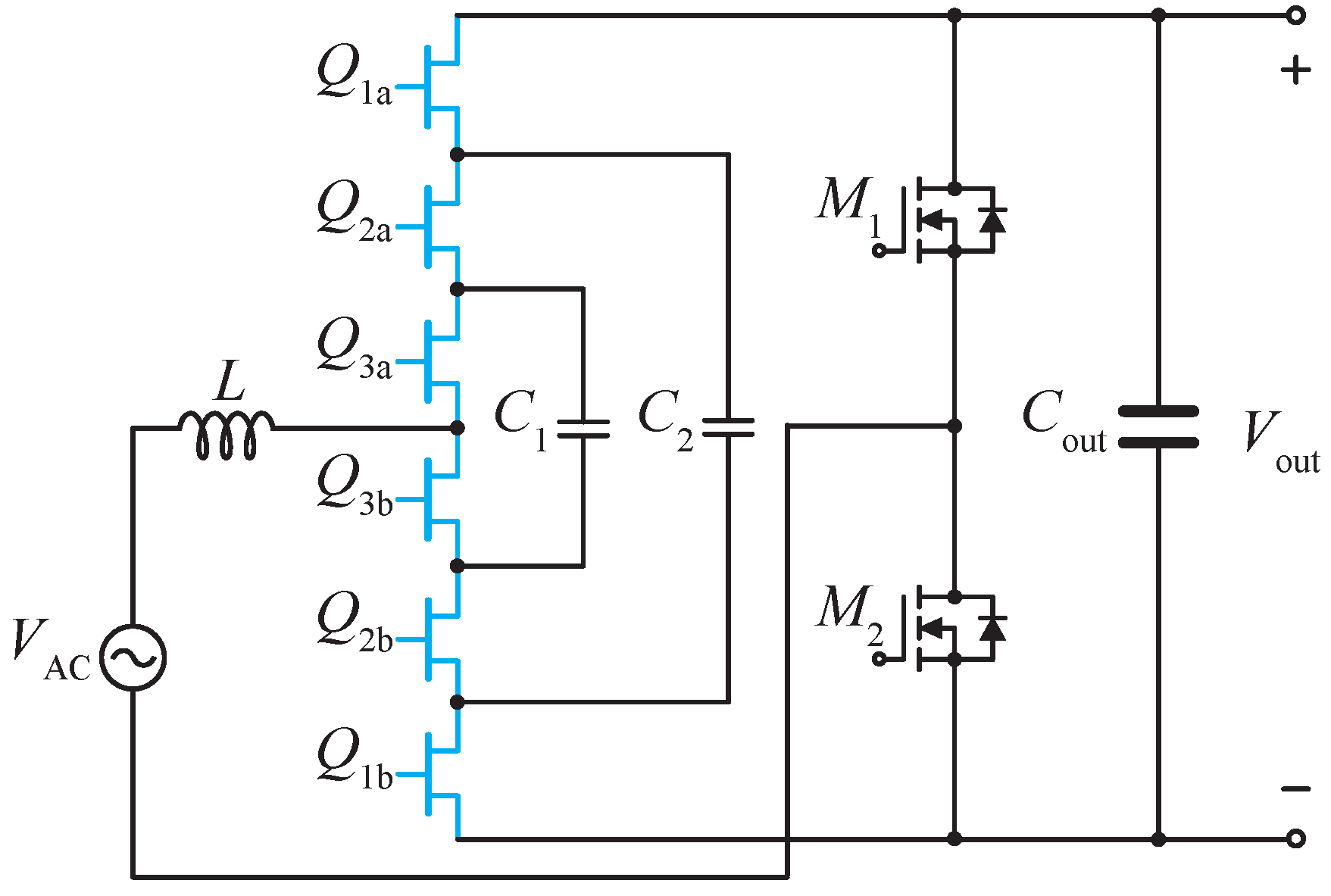
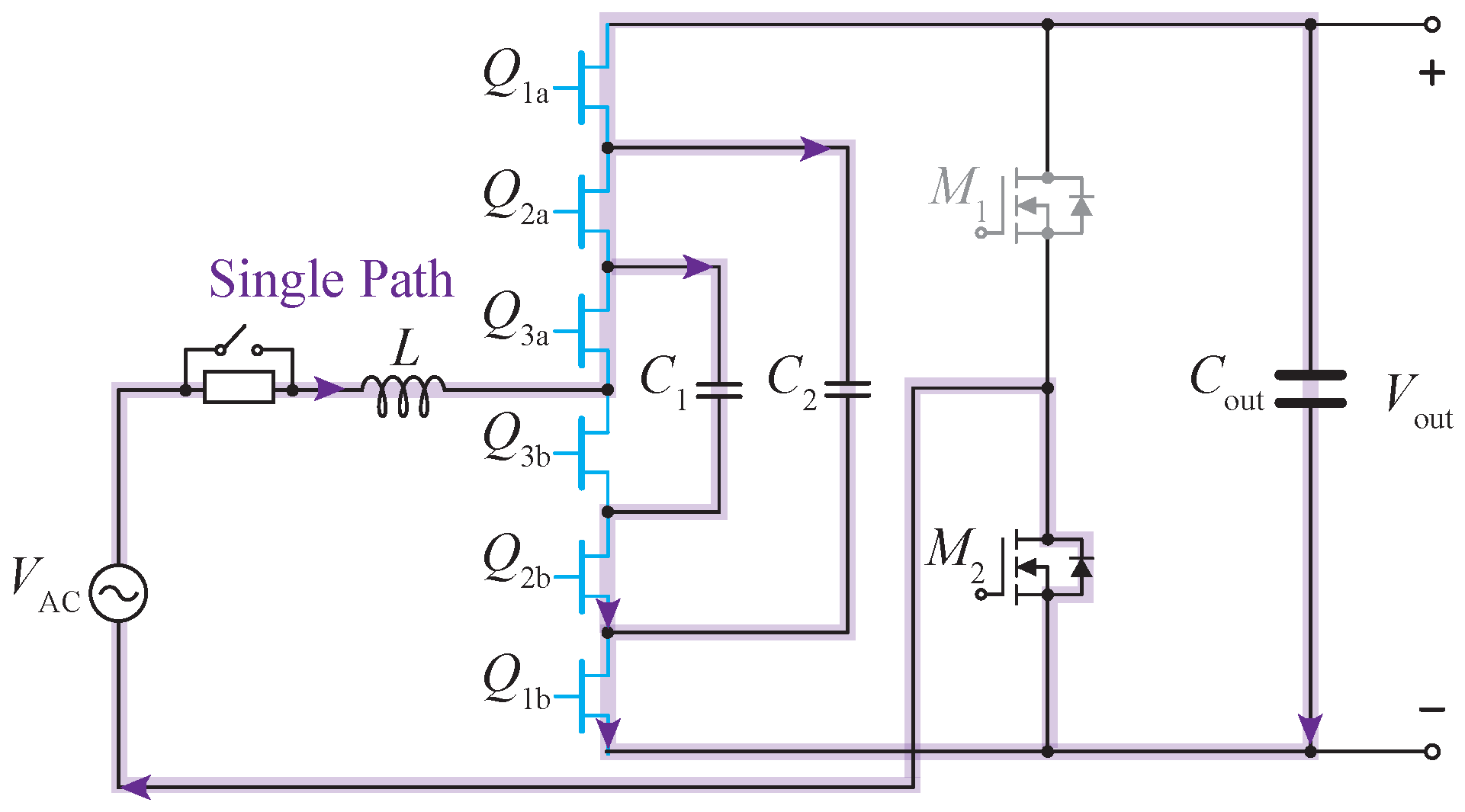
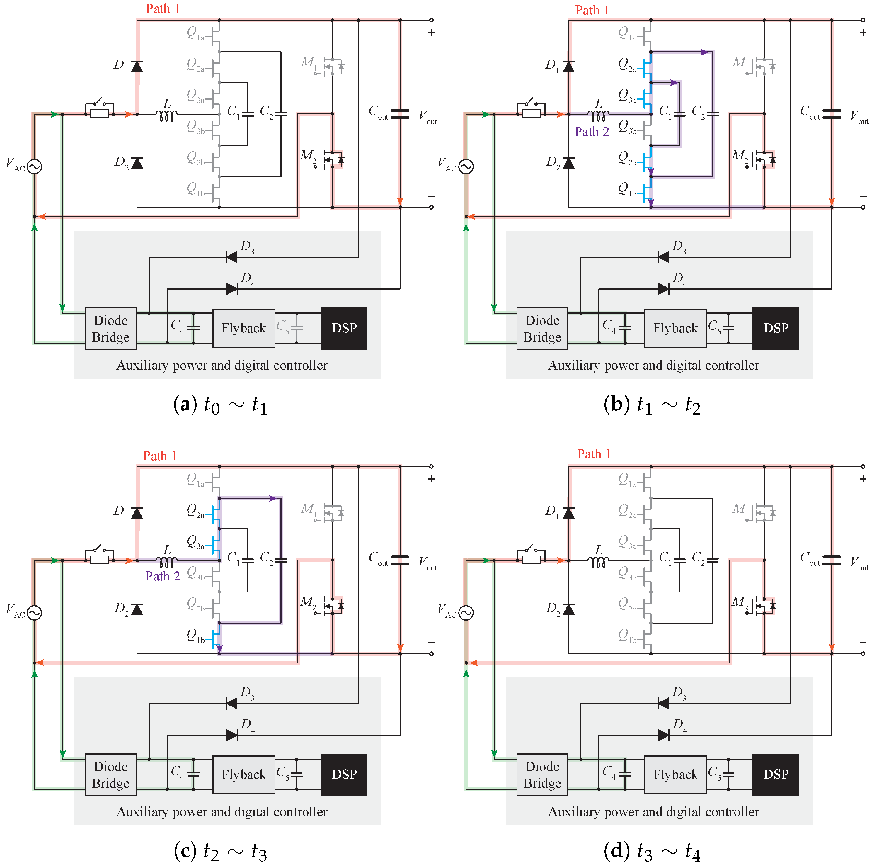
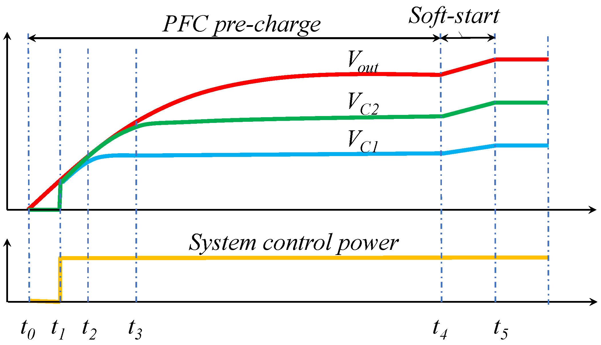
2. Multi-Path Precharging in Start-Up

The detailed circuit is shown in Figure 3. To limit the precharge inrush current, a current limiter is connected in series with the PFC main inductor. It will be bypassed by a relay when the precharge process ends. An auxiliary power circuit is designed and included in the system circuit, as well. The multi-step precharge method is proposed and shown in Figure 3. The main concept is to use additional low-cost Si diodes to divert the huge inrush current for charging the bulky DC link capacitors from the high-cost GaN devices.
The capacitors C 1 , C 2 and C o u t have to be charged to V o u t / 3 , 2 V o u t / 3 and V o u t , respectively, during start-up. The proposed multi-path and multi-step precharge method can be summarized with the following four steps.
Step 1 (Path 1): DC link charge and auxiliary power start [ t 0 to t 1 ]: AC grid voltage is applied to the PFC, and the current limiter is not bypassed. As shown in Figure 3a, Path 1 is formed for the grid voltage to charge output capacitor through the additional Si diodes, the body-diodes of the Si MOSFETs, and the current limiter. The flyback input capacitor is also charged by the grid through a diode bridge. Since the flyback input capacitor only has a value of several micro-farads, the input voltage builds up quickly and a 12 V control power supply is quickly established by t 1 . The flyback converter will continue to consume power from the AC grid until the whole precharge process ends.
Step 2 (Path 1 and 2): Charge DC link and two flying capacitors [ t 1 to t 2 ]: After the control power established at t 1 , Q 1 b and Q 2 b are turned on to form a charging path for both flying capacitors, as shown in Figure 3b. Capacitors C 1 and C 2 will be charged together with the DC link capacitors, and their voltages are the same. The two flying capacitors will be charged through Path 2, as shown in Figure 3b. The output capacitor voltage is still charged through Path 1. The GaN device voltage stresses in this step are shown below. This step ends when the inner flying capacitor C 1 is charged to one third of the AC input peak voltage V i n p e a k / 3 at t 2 . The voltage stress of Q 3 b will increase to one third of AC input peak voltage V i n p e a k / 3 by t 2 . Other devices’ voltages are 0 during this step.
V Q 1 a = 0 ; V Q 2 a = 0 ; V Q 3 a = 0 ; V Q 3 b = V C 1 ; V Q 2 b = 0 ; V Q 1 b = 0 ;
Step 3 (Path 1 and 2): Charge DC link and one flying capacitor [ t 2 to t 3 ]: Q 2 b is turned off at t 2 to ensure the capacitor C 1 remains at one third of the AC input peak voltage, as shown in Figure 3c. Q 1 b maintains the on state and capacitor C 2 is charged through Path 2 including Q 1 b . The C 2 voltage still follows the output capacitor voltage. The output capacitor voltage is still charged through Path 1. The GaN device voltage stresses during this stage are shown below. This step ends when C 2 voltage is charged to two thirds of AC input peak voltage 2 V i n p e a k / 3 at t 3 . By t 3 , the voltage stress of Q 2 b will increase to one third of AC input peak voltage V i n p e a k / 3 . During this step, the voltage stress of Q 3 b stays at one third of AC input peak voltage V i n p e a k / 3 , and other devices’ voltages are 0.
V Q 1 a = 0 ; V Q 2 a = 0 ; V Q 3 a = 0 ; V Q 3 b = V i n p e a k 3 ; V Q 2 b = V C 2 V i n p e a k 3 ; V Q 1 b = 0 ;
Step 4 (Path 1): Charge DC link [ t 3 to t 4 ]: Q 1 b is turned off at t 3 , as shown in Figure 3d. C 1 and C 2 will remain at V i n p e a k / 3 and 2 V i n p e a k / 3 respectively. Output capacitor continues to be charged through Path 1. At the end of this step, the output capacitor is charged to the AC input peak voltage V i n p e a k . The device voltage stress during this stage is shown below. The system precharge process ends at t 4 . The voltage stress of Q 1 b will increase to one third of AC input peak voltage V i n p e a k / 3 by t 4 . During this step, the voltage stresses of Q 3 b and Q 2 b stay at one third of AC input peak voltage V i n p e a k / 3 , and other devices’ voltages are still 0.
V Q 1 a = 0 ; V Q 2 a = 0 ; V Q 3 a = 0 ; V Q 3 b = V i n p e a k 3 ; V Q 2 b = V i n p e a k 3 ; V Q 1 b = V i n 2 V i n p e a k 3
According to the analysis above, the highest voltage stress of any GaN device during the precharge process is one third of the AC input peak voltage. Assuming the AC RMS voltage is 240 V, then the highest voltage stress is only 113 V. Later in the steady-state operation, the voltage stress of any GaN device in this circuit is one third of the DC link voltage ( 400 V / 3 = 133 V ) . The voltage rating of the selected GaN device in the hardware is 200 V, which provides enough safety margin. According to the above multi-path and multi-step precharge method, the expected output and flying capacitor voltages are plotted in Figure 4. The system goes into the soft-start stage after the proposed precharge process. During the soft start, flying capacitors C 1 and C 2 will be naturally balanced and their voltage will increase accordingly with the output voltage, because of the natural voltage balance mechanism of the FCML converter operation and phase-shift PWM.

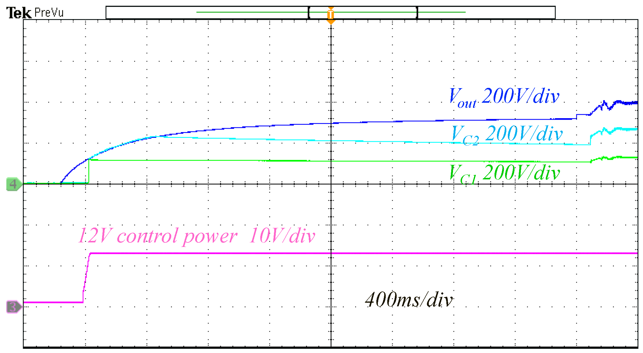
3. Testing and Verification

To verify the proposed multi-step and multi-path precharge method, we conducted detailed testing on a four-level GaN FCML Totem-Pole PFC. The specifications for the hardware are summarized in Table 1. We used EPC2047 for the GaN device, which is a 200 V / 10 m Ω device. The Si MOSFET is IPT60R028G7XTMA1, rated at 650 V / 28 m Ω , whereby two such MOSFETs are used in parallel for M1 and M2. We used single-phase AC power source (Chroma 61605) and DC resistive load bank for testing. The experimental waveforms are shown in Figure 5. From the tested waveforms, we can clearly see the flying capacitor and output capacitor voltages’ precharging process. The voltages of flying capacitors will follow the output capacitor voltage until their voltage reaches 1/3 and 2/3 of the AC input peak voltage, respectively. After that, the output capacitor voltage will be charged to the AC input peak voltage. Then, the system enters the soft-start process. The testing waveform fully verifies the proposed multi-step-and-multi-path precharge method.

4. Conclusions

In this paper, we proposed, developed and tested a multi-path and multi-step precharge method for GaN FCML Totem-Pole PFC. In the state-of-the-art precharge method, the GaN devices would be in the same charging path for charging the bulky DC capacitors, leading to a high inrush current through GaN devices. We propose to use two additional low-cost Si diodes to divert the high inrush charging current from the GaN devices. Therefore, the system has two precharge paths. One is through the Si diodes and the body-diodes of the Si MOSFETs, which are more than enough to handle the high inrush current for charging the bulky DC capacitors. The other path is through the GaN devices and the body-diodes of the Si MOSFETs to only handle very low inrush current for charging the very small high-frequency flying capacitors. The proposed method significantly improves the reliability of the high-cost GaN devices during the precharge process for GaN FCML Totem-Pole PFC. Finally, the experimental results verified the proposed method.

Author Contributions

Conceptualization and validation, Q.M.; investigation, Q.M. and Q.H.; writing—original draft preparation, Q.M. and Q.H.; writing—review and editing, Q.H. and F.M.; visualization, Q.M. and F.M.; supervision, A.Q.H.; project administration, A.Q.H. and M.A.d.R. All authors have read and agreed to the published version of the manuscript.

Funding

This research was funded by the Efficient Power Conversion Corporation.

Data Availability Statement

The original contributions presented in this study are included in the article. Further inquiries can be directed to the corresponding author.

Conflicts of Interest

Author Michael A. de Rooij was employed by the company Efficient Power Conversion Corporation (EPC). The remaining authors declare that the research was conducted in the absence of any commercial or financial relationships that could be construed as a potential conflict of interest.

References

  1. Liu, Z.; Lee, F.C.; Li, Q.; Yang, Y. Design of GaN-Based MHz Totem-Pole PFC Rectifier. IEEE J. Emerg. Sel. Top. Power Electron. 2016, 4, 799–807. [Google Scholar] [CrossRef]
  2. Liu, Z.; Huang, Z.; Lee, F.C.; Li, Q. Digital-Based Interleaving Control for GaN-Based MHz CRM Totem-Pole PFC. IEEE J. Emerg. Sel. Top. Power Electron. 2016, 4, 808–814. [Google Scholar] [CrossRef]
  3. Saglam, B.; Aksit, M.H.; Tamyurek, B. A Comparison of GaN-Based Cascode and E-mode HEMTs Using Bridgeless Totem Pole PFC. In Proceedings of the 2022 IEEE Energy Conversion Congress and Exposition (ECCE), Detroit, MI, USA, 9–13 October 2022; pp. 1–6. [Google Scholar] [CrossRef]
  4. Sun, J.; Huang, X.; Strain, N.N.; Costinett, D.J.; Tolbert, L.M. Inductor Design and ZVS Control for a GaN-Based High Efficiency CRM Totem-Pole PFC Converter. In Proceedings of the 2019 IEEE Applied Power Electronics Conference and Exposition (APEC), Anaheim, CA, USA, 17–21 March 2019; pp. 727–733. [Google Scholar] [CrossRef]
  5. Sun, J.; Gui, H.; Li, J.; Huang, X.; Strain, N.; Costinett, D.J.; Tolbert, L.M. Mitigation of Current Distortion for GaN-Based CRM Totem-Pole PFC Rectifier With ZVS Control. IEEE Open J. Power Electron. 2021, 2, 290–303. [Google Scholar] [CrossRef]
  6. Lee, J.Y.; Chen, J.H.; Lo, K.Y. Design of a GaN Totem-Pole PFC Converter Using DC-Link Voltage Control Strategy for Data Center Applications. IEEE Access 2022, 10, 50278–50287. [Google Scholar] [CrossRef]
  7. Wang, S.; Pham, P.H.; Li, Q.; Chen, X. PCB-Based Magnetics Integration and Common-Mode Noise Suppression for A High-Frequency PFC. In Proceedings of the 2023 IEEE Applied Power Electronics Conference and Exposition (APEC), Orlando, FL, USA, 19–23 March 2023; pp. 2043–2049. [Google Scholar] [CrossRef]
  8. Huang, Q.; Ma, Q.; Liu, P.; Huang, A.Q.; de Rooij, M.A. 99% Efficient 2.5-kW Four-Level Flying Capacitor Multilevel GaN Totem-Pole PFC. IEEE J. Emerg. Sel. Top. Power Electron. 2021, 9, 5795–5806. [Google Scholar] [CrossRef]
  9. Stillwell, A.; Pilawa-Podgurski, R.C.N. A Five-Level Flying Capacitor Multilevel Converter With Integrated Auxiliary Power Supply and Start-Up. IEEE Trans. Power Electron. 2019, 34, 2900–2913. [Google Scholar] [CrossRef]
  10. Jiao, D.; Huang, A.Q. Pre-Charge Strategy and Light-Load Voltage Balance Enhancement for DC/AC Flying Capacitor Converter. In Proceedings of the 2024 IEEE Texas Power and Energy Conference (TPEC), College Station, TX, USA, 12–13 February 2024; pp. 1–6. [Google Scholar] [CrossRef]
  11. Maier, J.; Ulrich, B.; Czerwenka, P.; Hennig, E.; Schullerus, G. A Start-Up Method for Flying Capacitor Topologies Using the Output Filter with few Additional Components. In Proceedings of the 2024 IEEE Energy Conversion Congress and Exposition (ECCE), Phoenix, AZ, USA, 20–24 October 2024; pp. 3465–3472. [Google Scholar] [CrossRef]
  12. Janik, D.; Kosan, T.; Kamenicky, P.; Peroutka, Z. Universal precharging method for dc-link and flying capacitors of four-level Flying Capacitor Converter. In Proceedings of the IECON 2013–39th Annual Conference of the IEEE Industrial Electronics Society, Vienna, Austria, 10–13 November 2013; pp. 6322–6327. [Google Scholar] [CrossRef]
  13. Sepahvand, H.; Khazraei, M.; Corzine, K.A.; Ferdowsi, M. Start-up Procedure and Switching Loss Reduction for a Single-Phase Flying Capacitor Active Rectifier. IEEE Trans. Ind. Electron. 2013, 60, 3699–3710. [Google Scholar] [CrossRef]
  14. Ghias, A.M.Y.M.; Pou, J.; Agelidis, V.G.; Ciobotaru, M. Initial Capacitor Charging in Grid-Connected Flying Capacitor Multilevel Converters. IEEE Trans. Power Electron. 2014, 29, 3245–3249. [Google Scholar] [CrossRef]
Figure 1. Topology of four-level flying-capacitor PFC.
Electronics 14 02637 g001
Figure 2. The traditional single-path precharge process [12].
Electronics 14 02637 g002
Figure 3. Operation principle of proposed multi-path precharge method.
Electronics 14 02637 g003
Figure 4. Voltage of capacitors under proposed method.
Electronics 14 02637 g004
Figure 5. Flying capacitor voltage during system start-up (there is a limited bandwidth on the waveforms due to the long time frame).
Electronics 14 02637 g005
Table 1. Hardware specifications.
ParametersValue
Input voltage240  V rms
Output voltage400 V
Switch frequency120 kHz
Inductor13 μH
Output capacitor660 μF
Flying capacitor≤4.4 μF
Disclaimer/Publisher’s Note: The statements, opinions and data contained in all publications are solely those of the individual author(s) and contributor(s) and not of MDPI and/or the editor(s). MDPI and/or the editor(s) disclaim responsibility for any injury to people or property resulting from any ideas, methods, instructions or products referred to in the content.

