Article

Research on Improving the Avalanche Current Limit of Parallel SiC MOSFETs

1
State Grid Sichuan Electric Power Research Institute, Chengdu 610041, China
2
State Key Laboratory of Power Transmission Equipment Technology, Chongqing University, Chongqing 400044, China
3
State Key Laboratory of Disaster Prevention & Reduction for Power Grid, Changsha University of Science and Technology, Changsha 410205, China
*
Authors to whom correspondence should be addressed.
Electronics 2025, 14(13), 2502; https://doi.org/10.3390/electronics14132502
Submission received: 19 May 2025 / Revised: 16 June 2025 / Accepted: 17 June 2025 / Published: 20 June 2025

Abstract

:
The transient overvoltage caused by coupling of loop inductance during rapid turn off of a silicon carbide metal-oxide-semiconductor field-effect transistor (SiC MOSFET) can easily induce avalanche breakdown. Meanwhile, the instantaneous high-density heat flux generated by energy dissipation can create significant electrothermal coupling stress, potentially leading to device failure under severe conditions. To address the issue that the multi-chip parallel structure of power modules cannot linearly enhance avalanche withstand capability, an innovative device screening method based on parameter matching is proposed in this paper. The effectiveness of the proposed solution is verified through experiments, with the total current limit of dual-tube parallel devices and three-tube parallel devices achieving 1.9 times and 2.4 times that of single-tube devices, respectively. This research is of great significance for improving safe and reliable operation of the system.

1. Introduction

Silicon carbide metal-oxide-semiconductor field-effect transistors (SiC MOSFETs) have become the core components of the new generation of power and electronic systems due to their high power density, excellent thermal conductivity, and high-frequency switching capability [1,2]. They are widely used in high-temperature, high-voltage, and high-frequency application scenarios such as electric vehicle drives and smart grids. However, their fast switching characteristics can cause the rapidly changing drain current to interact with the parasitic inductance of the loop when the devices are turned off, inducing transient overvoltage spikes (up to 1.2–1.5 times the rated voltage). The strong coupling effect of electrical and thermal stress makes the devices easily enter the avalanche breakdown, and local hot spots are formed in the active region of the chip, seriously threatening the reliability of the devices [3,4]. Power devices may not necessarily fail directly after avalanche breakdown, as SiC MOSFETs can withstand repeated avalanches [3,5]. In this paper, the maximum current the devices can withstand before avalanche failure is defined as the avalanche current limit.
Parallel/series chips are often used to increase the modules’ current/voltage rating to meet higher power applications. In theory, parallel connection of n devices can increase the rated current by n times, but in reality, the enhancement of avalanche tolerance exhibits significant sub-linear characteristics [6]. Such a nonlinear degradation phenomenon originates from the inherent discreteness of device parameters and the asymmetry of experimental condition parameters, which can lead to an imbalance in dynamic current distribution [7]. In addition, devices carrying higher current inevitably dissipate most energy stored in inductance as heat. Under the action of high current and high temperature, the performance may be affected [8], and the reliability of power devices will be greatly challenged [6]. Therefore, increasing the current avalanche limit for power devices will positively influence the safe and stable operation of devices and systems.
The current research on improving the avalanche capability of power devices focuses on packaging and chips. The packaging optimization reduces parasitic inductance and improves thermal resistance through ribbon bonding, nano-silver sintering, and a symmetric direct-bonded copper (DBC) layout [9,10,11]. The breakthroughs at the chip level are reflected in the innovation of cell structure and process optimization. Zhu et al. [12] found that the presence of the P ring in the cellular structure can reduce the collision ionization rate at the bottom of the field oxide. Ren et al. [13] and Zhao et al. [14] proposed several cell parameter designs for SiC MOSFETs to improve avalanche capability. Kim et al. [15] successfully fabricated 1.2 kV SiC MOSFETs with different P+ region designs and studied the impact of P+ region on the avalanche energy of SiC MOSFETs. References [16,17,18] proposed optimized structures, obtained the optimal structure parameters through simulation, and verified the collision ionization rate and electric field distribution under these parameters. Wu et al. [19] established a half-cell model using technology computer-aided design (TCAD) and analyzed and compared the differences in avalanche energy distribution among linear, square, and hexagonal cell topologies. Optimization has been extended to device fabrication and layout designs, with controlled annealing temperature and duration demonstrating significant effects on avalanche performance [20,21].
Currently, much research is based on single-tube or parallel devices’ avalanche reliability and withstand voltage capability [22,23,24], and most of them are only compared under different inductance or temperature conditions. Takamori proposed a method to enhance the avalanche capability of the device by parallel connection of SiC diodes [25]. However, there is relatively little research on methods for improving the avalanche capability of parallel devices. Through simulation and experimental analysis, [6] found that the difference in breakdown voltage (ΔBV) is the main cause of avalanche failure in parallel devices. Devices with a smaller BV will receive more current and heat through current sharing and eventually fail first. Herrmann [26] and Fayyaz [27], respectively, investigated how parallel connection of devices with different BVs can reduce the total avalanche tolerance.
Based on this, to improve the avalanche capability of parallel devices during operation, a device screening method based on parameter matching is proposed and verified through experiments in this paper. Firstly, the avalanche impact characteristics of power devices are described, and the breakdown voltage is defined. Secondly, an experimental protocol was designed with commercial SiC MOSFET chips as the research object, and a parallel avalanche experimental platform was established to quantify current-sharing characteristics across parallel devices at varying current levels. Finally, an optimized parameter screening approach was developed and experimentally validated.

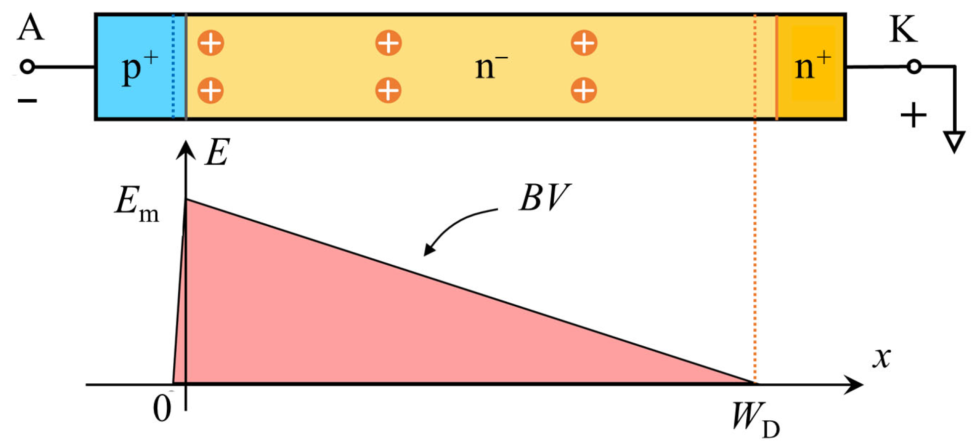
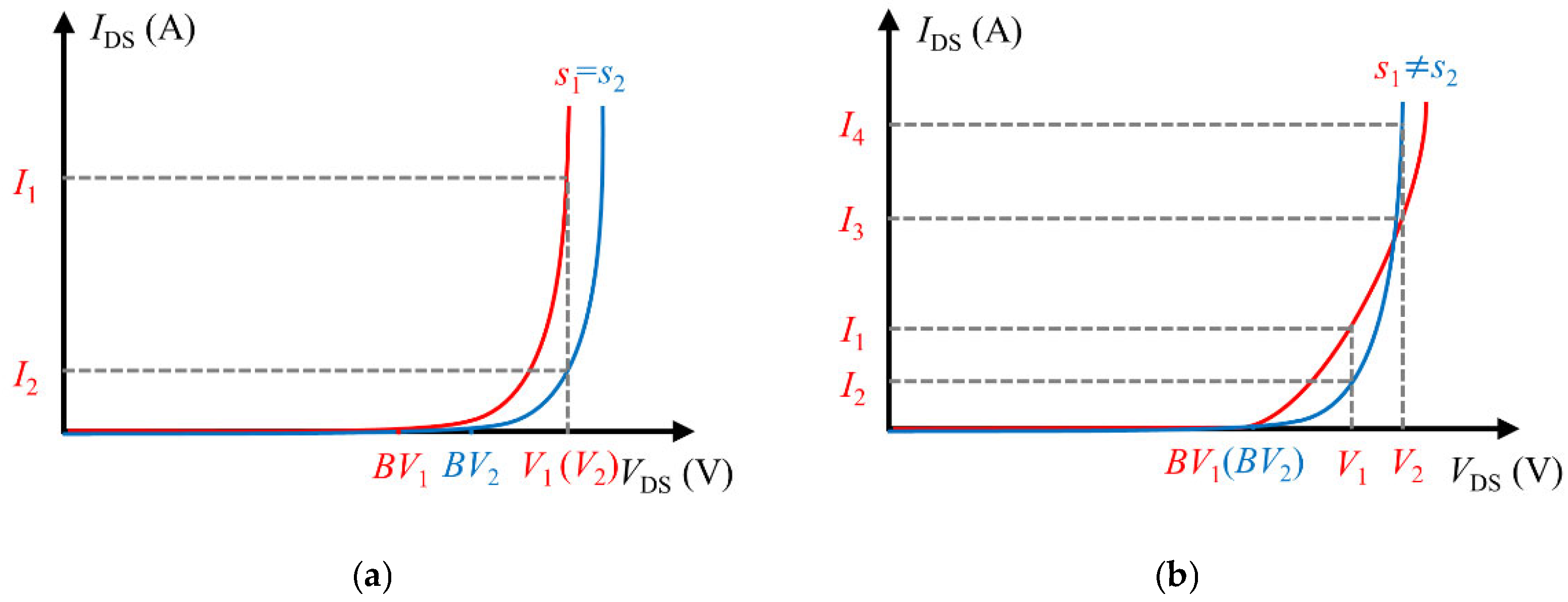
2. Principle of Avalanche Breakdown of Power Devices

Under strong electric field conditions, charge carriers in semiconductors will accelerate under the action of the electric field. This gives some charge carriers enough kinetic energy to collide with lattice atoms, and these charge carriers transfer energy to electrons in the valence band through collision, causing ionization and generating electron–hole pairs. This process is called collision ionization. Subsequently, the generated electrons and holes continue to move in opposite directions under the action of the electric field. The electric field accelerates them, and they collide with other valence electrons to generate new electron–hole pairs. In this way, many charge carriers can be multiplied, and avalanche breakdown will occur when the multiplication is enhanced to a certain extent.
Figure 1 shows a positive–intrinsic–negative (PiN) diode. When the voltage is applied in reverse across the devices, the built-in potential gradually increases, and the width of the depletion layer in the intrinsic region gradually lengthens. The electric field distribution formed in the barrier region is derived from the Poisson equation as [28]:
d 2 ψ i d x 2 = d ξ d x = q ε s N D x n x N A x + p x
( ε s ( E ) ) = q N D
where ψ i is the electric potential, and ξ is the electric field. The slope calculated according to the electric field-depletion layer width formula is
d E d x = q N D ε s
E m W D = q N D ε s
where N D and N A are the donor and acceptor concentrations of ionization, respectively, n and p are the electron and hole concentrations, respectively, and ε s is the dielectric constant. When charge carriers generate at least one pair of electron–hole pairs when passing through the depletion layer, an avalanche is considered to occur,
0 W D α d x = 1
where α is the collision ionization coefficient. The magnitude of the reverse voltage is the breakdown voltage area enclosed by the electric field and depletion region, as shown in Figure 1. Since the concentration in the p+ region is much higher than that in the n− region, the breakdown voltage area is approximately
B V = 1 2 W D E m = ε s E m 2 2 q N D
Generally, the avalanche BVs of Si and SiC devices are relatively high. It is defined as the voltage value when a reverse current of 1 mA passes through the device when it is turned off. The blocking characteristic curve at the time of turn-off has a distinct corner near the breakdown voltage, and the current suddenly increases. At this time, the devices undergo a hard avalanche breakdown. The rising slope of the breakdown curve can be represented by the hardness s. If it is steep, it is called hard; if the rising slope is gentle, it is called soft. Figure 2 shows that the devices with the same model may exhibit differences in blocking voltage and breakdown curve hardness due to the differences in manufacturing processes. As shown in Figure 2a, when the blocking voltage is different but the hardness is the same, more current is shared with a lower blocking voltage when connected in parallel. Figure 2b shows that when the hardness is different but the blocking withstand voltage is the same, the parallel current sharing will show differences under different loads.

3. Avalanche Test of Power Devices

3.1. Principle of UIS Avalanche Test

Unclamped inductive switching (UIS) is commonly used in academia for avalanche testing. This is a method used to simulate transient avalanches encountered by devices in system applications. Through this test, the ability of the devices to withstand the energy of a single avalanche can be obtained, and it is also an important indicator for measuring the reliability of power devices. The energy stored in the load inductor must be completely released when the devices are turned off. At this time, the devices are subjected to high voltage and high current, and the energy generated instantly can easily cause device failure. During the process of energy increasing, the energy endured by the device for the last time before failure is usually taken as the single pulse avalanche energy, and the current at this time is taken as the avalanche current limit.
The simplified schematic diagram and ideal output waveform of the UIS test system are shown in Figure 3, where the device under test (DUT) represents a SiC MOSFET. S is a device that can achieve quick disconnection, and SiC MOSFET is used as a substitute in the experiment. Meanwhile, S is also used as a protective component. When the current sensor detects the overcurrent signal, the protective component can be controlled to cut off the main loop. The voltage source VC can provide a constant voltage ranging from 0 to 400 V, and the impulse source VG can provide an ideal voltage square wave ranging from −30 to 30 V. The inductor L is an energy storage carrier during charging, and the diode D can provide a release path for current during the DUT avalanche. Here, to improve the energy release rate, a resistance is connected in parallel next to the diode.
SiC MOSFETs SCT3120AL from ROHM (Kyoto, Japan) are used to perform a dynamic blocking characteristic test in this paper. For ROHM SiC MOSFET SCT3120AL, the rated drain-source current at 25 °C is 21 A, packaged in standard TO-247, and Figure 4 shows the half-cell structure of a trench gate SiC MOSFET. To ensure a breakdown voltage higher than 650 V, the thickness of the epitaxial layer is designed to be 7 μm, the width of a single cell is 3.77 μm, and the depth and width of the gate trench are 1 μm and 0.54 μm. The thickness of the gate oxide is 60 nm, and the doping concentration of the n drift region is 1 × 1016 cm−3.
When S and the DUT are driven to a high potential, the constant voltage source VC charges the SiC MOSFET through the inductor. The gradually increasing loop current ID can be obtained in the following way:
d I D = V C L d t
When the preset charging time is reached, the loop current increases to IAV, and the DUT is turned off. At this time, the energy stored in the inductor will be fully sustained by the DUT. As the switch is quickly turned off, the high di/dt and inductive coupling generate instantaneous high voltage, which is applied to the device. The current continues to flow through the diode until the ID returns to zero, marking the completion of a single pulse avalanche. The instantaneous high voltage generated can be expressed as follows:
V BR = L d i d t
At this time, due to the simultaneous disconnection of the DUT and the quick switch S, the avalanche time (tAV) can be expressed as follows:
t AV = I AV V BR L
Finally, when the avalanche discharge process is completed, the single-pulse avalanche ends, where the single avalanche energy (EAV) is obtained from Equation (10):
E AV = 0 t AV I D ( t ) × V DS ( t ) d t = 1 2 I AV × V BR × t AV = 1 2 I AV 2 L

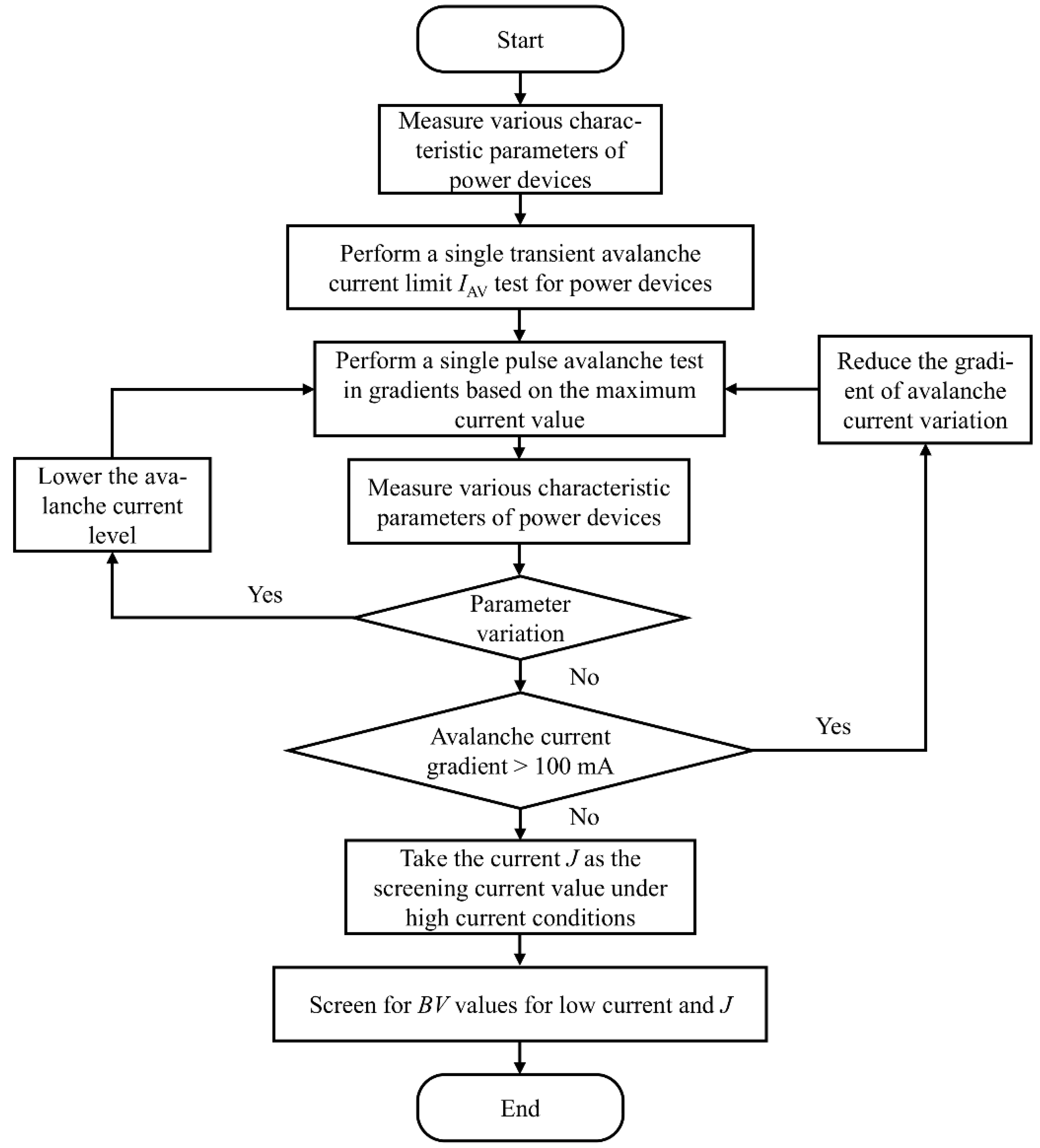
3.2. Design of UIS Avalanche Test Plan

Figure 5 shows the UIS test platform, which includes a power supply, test circuit, control panel, auxiliary power supply, inductive load, and electrical parameter test equipment Agilent B1505A and Agilent N1265A (Santa Clara, CA, USA). The equipment has been listed in Table 1. Figure 6 shows the avalanche waveform of single-tube SiC MOSFETs, which can withstand repeated avalanches and operate normally without exceeding the current limit in a single avalanche. Currently, the inductance is 1 mH, and the charging voltage is 40 V. After charging for 100 μs, the avalanche current reaches 4 A, and the avalanche voltage clamps at 1380 V. Here, the Tektronix TCP0030A and Tektronix THDP0100 (Portland, OR, USA) are used to monitor current and voltage in real time. In addition, a handheld infrared (IR) thermography FLIR E5 (Wilsonville, OR, USA) is used for temperature monitoring during the experimental process.
Figure 7 and Figure 8 show the current distribution when SiC MOSFETs with different BVs are connected in parallel. Figure 7a or Figure 8a show the avalanche current sharing when two and three SiC MOSFETs are connected in parallel under low-current conditions, respectively. Figure 7b and Figure 8b show the avalanche current sharing when two and three SiC MOSFETs are connected in parallel under high-current conditions, respectively. It can be seen that the devices have uneven current sharing due to inconsistent BVs, and the current sharing may also change under different total currents. This confirms the difference in hardness of the blocking characteristic curve described in Figure 2.

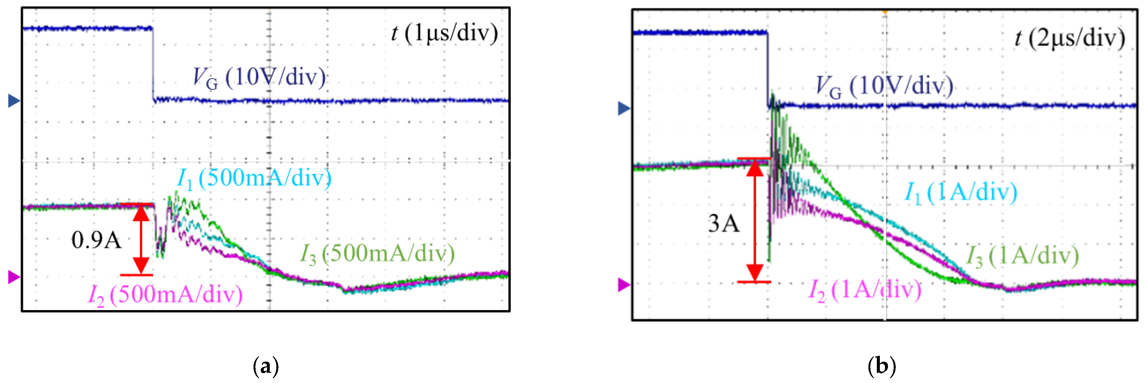
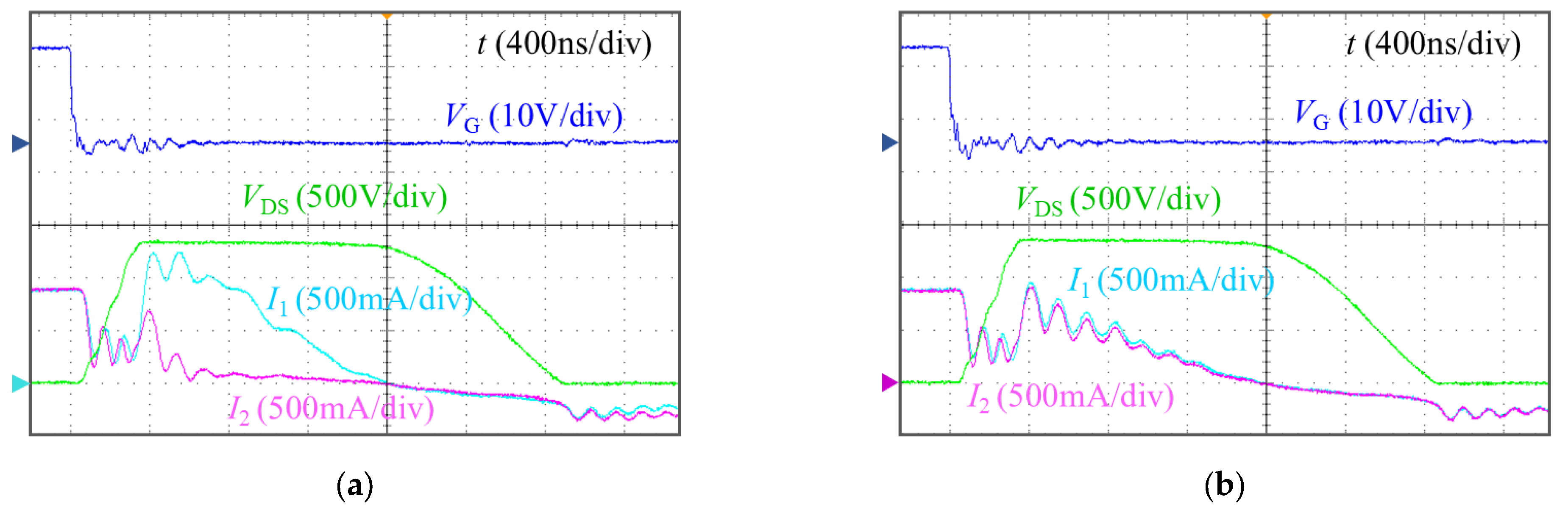
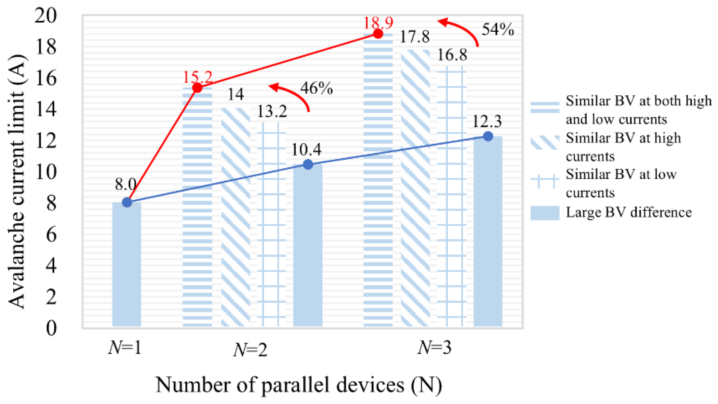
4. Proposal and Verification of Methods for Improving Parallel Avalanche Capability

Currently, the device parallel screening strategy in the industrial sector focuses on static parameter consistency. The Agilent B1505A power analyzer is used to detect static parameters such as threshold voltage and on-resistance, and the static blocking voltage when the drain-source current equals 1 mA, and these parameters are used as the screening criteria, ensuring consistent parallel current sharing and achieve the matching of parasitic branch parameters. Although this plan can maintain the current balance under normal operating conditions, the avalanche of SiC MOSFET devices usually occurs during the dynamic turn-off process with high current and high junction temperature. At this time, the blocking voltage of the devices shows a significant positive temperature coefficient. In addition, due to different device process parameters, the blocking voltage’s changing rate is also different. This leads to a significant deviation between the static and dynamic avalanche voltage. A dynamic dual-mode screening mechanism is proposed in this research: based on maintaining static parameter matching, an avalanche blocking voltage test parameter is added. The UIS test platform is used to simulate avalanche conditions and captures the dynamic blocking voltage during transient avalanche processes under high currents.
SiC MOSFETs SCT3120AL from ROHM (Kyoto, Japan) are used as DUTs. Their blocking curve shows significant nonlinear characteristics, with substantial deviations in drain-source voltage between low-current (ID = 1 mA) and high-current operating conditions. Selecting devices with low-hardness blocking characteristics to construct parallel systems makes exposing the dynamic avalanche current-sharing failure mechanism easier. Figure 9 shows the screening method for parallel avalanche devices, with the implementation details elaborated step-by-step below:
(a)
Firstly, an Agilent B1505A is used to test the static parameters of a large number of SCT3120AL. The electrical characteristic curves, such as the forward I-V curve when VG = 18 V and Ttest = 25 °C, and the reverse I-V curve when VG = −4 V and Ttest = 25 °C, and the threshold voltage are tested after the drain electrode and the gate electrode are shorted; the drain-source voltage is the threshold voltage when the drain-source is 10 mA.
(b)
In addition, the blocking characteristic curve is tested for all devices, and the drain-source voltage at ID = 1 mA is selected as the low-current BV.
(c)
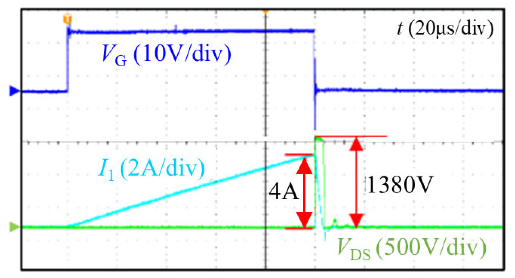
Parts of SiC MOSFETs are selected for single avalanche current limit testing to determine the current limit IAV of the device. The charging duration is maintained at 100 μs, and the charging voltage is continuously increased for the UIS test until the device fails. After multiple tests, the IAV of the selected DUT is around 8 A.
(d)
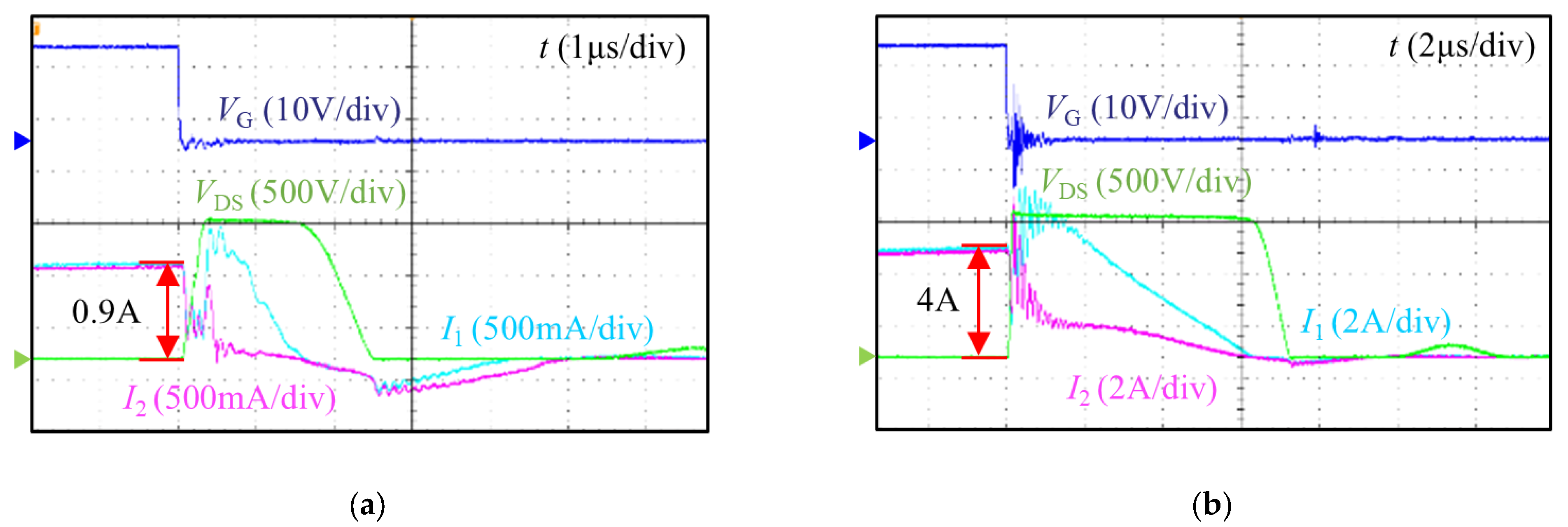
Some SiC MOSFETs are selected to perform avalanche at different avalanche current levels, with three devices used for comparison at each current level. Taking the selected DUT as an example, after three tests are performed at avalanche current levels of 7 A, 6.5 A, and 500 mA, respectively, the static electrical parameters are tested and recorded.
(e)
For devices that have not undergone numerical changes, the current range is narrowed, and the maximum value is continuously approached. Screening is stopped when the avalanche current gradient is less than 100 mA.
(f)
The final result is that the devices will experience an avalanche at 900 mA without significantly changes; therefore, devices with similar BVs measured at 1 mA and 900 mA are selected for parallel avalanche.
After implementing parameter matching for commercial SiC MOSFETs based on this scheme, a dynamic avalanche verification is performed using the UIS test platform. Figure 10 compares the breakdown voltage characteristics of 40 sets of SiC MOSFETs: the BV values show significant dispersion under static test (1 mA) and dynamic avalanche (900 mA) conditions. The data analysis shows that only 37.5% of the samples meet the synchronous matching requirements of static and dynamic breakdown voltages, confirming that static parameters cannot effectively predict high-current avalanche characteristics. This result highlights the necessity of dynamic screening.
Devices with different parameters are selected for parallel connection to explore the specific influence of the BV on current sharing. When group ① devices with comparable BVs at 1 mA and significant BVs at 900 mA are selected for parallel connection, as shown in Figure 11a, the current-sharing difference during avalanche is obvious. When group ② devices with different BVs at 1 mA and comparable BVs at 900 mA are selected to the avalanche parallel test, as shown in Figure 11b, the parallel current-sharing effect is good. This also indicates that screening only using the blocking voltage at low currents cannot achieve a good current-sharing effect. Group ③ and ④ devices with comparable blocking voltages at 900 mA and different blocking voltages at 1 mA are also selected for parallel connection at higher currents. Figure 11c shows the current-sharing effect of the two devices in parallel in group ③. When the current drops to the low-current range, the current-sharing difference becomes larger, and the energy distribution becomes uneven. Figure 11d shows the result of the parallel connection of three devices in group ④. As the number of parallel devices increases, even small parameter differences can lead to uneven current distribution. The parallel current-sharing characteristics are more sensitive to the number of parallel devices, which is also a major reason why increasing the number of parallel devices in engineering applications is difficult. Furthermore, since the current level during testing is higher than the current during screening, the parallel current-sharing capability has also been weakened.
According to the device screening method mentioned earlier, parallel limit tests are conducted for devices under four conditions: large BV difference, small BV difference at low currents and large BV difference at high currents, large BV difference at low currents and small BV difference at high currents, and small BV difference at both high and low currents. The avalanche limit currents with different numbers of parallel-connected devices are shown in Figure 12.
The limit of a single-tube avalanche current is 8 A. When devices with significant BV differences are connected in parallel, as the number increases, the avalanche current limit increases slowly as shown by the blue line in the figure. The total current limit of dual-tube parallel devices becomes 10.4 A, which is 1.3 times (ideally 2 times) that of a single device, while for three-tube parallel devices, it becomes 12.3 A, which is 1.54 times (ideally 3 times) that of a single device.
To improve the avalanche current for devices connected in parallel by screening the BV value of the devices, a current value must be selected. Screening BV under high current yields a higher avalanche current limit than screening it only under low current. However, when screening only one of the low or high current values, the avalanche current limit increases slightly.
The average single-tube avalanche limit can be further increased when considering the BV values under both high and low current before parallel connection. At this point, the total current limit of dual-tube parallel devices has become 15.2 A, which is 1.9 times that of single-tube devices, and the total current limit of three-tube parallel devices has become 18.9 A, which is 2.4 times that of single-tube devices. Similarly, compared with the traditional method that only screens the BV value obtained when ID = 1 mA, the avalanche current limit increases from 13.2 A to 15.2 A when two devices are in parallel, and the avalanche current limit increases from 16.8 A to 18.9 A when three devices are in parallel. This proves the effectiveness of the parameter screening strategy.
This research reveals the sub-linear attenuation of the avalanche current limit in multiple parallel SiC MOSFET systems, which is essentially derived from the inherent discreteness of device parameters and the nonlinear characteristics of breakdown voltage under dynamic operating conditions. The avalanche current limit decreases significantly as the number of parallel devices increases. Although the collaborative optimization plan based on multidimensional parameter screening can increase the avalanche current limit by 46% to 54%, the ideal effect is still not achieved. This is because the parameters screened in advance still have differences in accuracy. In addition, BV always changes under different currents and temperatures, and the pre-screened current levels are relatively low. The BV corresponding to the current when the devices experience an avalanche cannot be obtained and screened in advance and can only be infinitely approximated using this plan.
In summary, the innovation of this scheme lies in constructing a dynamic BV screening model, achieving progressive optimization of device matching accuracy and improving the parallel avalanche current limit. This provides a quantifiable parameter matching paradigm for the design of high-reliability power modules, while avoiding the complex process modifications and cost surges involved in traditional structural optimization schemes. The proposed method can be used in the future in high-speed switches, mechanical circuit breakers, and aerospace and automotive applications. In the future, it is necessary to try to manufacture chips with a harder blocking characteristic curve in the fabrication process. In this way, the difference in BV values between low and high currents is not too large, and the screening effect for low currents will be more obvious, which is also more conducive to parallel device connection.

5. Conclusions

With the continuous growth of the demand for device capacity in high-power electronic systems, the challenge in avalanche capability of multi-chip parallel architectures is becoming increasingly prominent. Research has found that the core mechanism of avalanche failure in parallel devices lies in the electrothermal coupling effect caused by the discreteness of breakdown voltage. Meanwhile, the breakdown voltage exhibits significant nonlinear characteristics during dynamic avalanche processes, making traditional static parameter matching strategies ineffective. In response to this challenge, this paper innovatively proposes a method for improving the avalanche current limit of parallel devices, which requires simultaneous screening and matching of BV under high- and low-current states. The result shows that the avalanche limit of dual-tube parallel devices increases from 1.3 times that of single-tube devices to 1.9 times after parameter screening, while the avalanche limit of three-tube parallel devices increases from 1.54 times to 2.4 times. The result provides a quantifiable engineering implementation path for the avalanche capability design of high-reliability power modules.

Author Contributions

Conceptualization, H.M. and L.T.; methodology, H.M.; software, B.W.; validation, H.M., B.W. and L.T.; formal analysis, J.C.; investigation, Y.X.; resources, Y.X.; data curation, B.W.; writing—original draft preparation, H.M.; writing—review and editing, L.T., B.W. and L.T.; visualization, J.C.; supervision, X.L.; project administration, X.L.; funding acquisition, H.M. All authors have read and agreed to the published version of the manuscript.

Funding

This research was funded by the Special Funding for Postdoctoral Research Projects of Sichuan Province, grant number TB2024063.

Data Availability Statement

The original contributions presented in the study are included in the article; further inquiries can be directed to the corresponding authors.

Conflicts of Interest

Authors Hua Mao, Xinsheng Lan, Yalong Xia and Junjie Chen were employed by the company State Grid Sichuan Electric Power Research Institute. The remaining authors declare that the research was conducted in the absence of any commercial or financial relationships that could be construed as a potential conflict of interest.

References

  1. Long, Y.; Chen, Y.; Wang, P.; Hou, B.; He, H. A novel insight into the mechanism of bipolar degradation in 4H-SiC MOSFET. IEEE Electron Device Lett. 2025, 46, 464–467. [Google Scholar] [CrossRef]
  2. Kim, M.; Forbes, J.J.; Hirsch, E.A. Evaluation of long-term reliability and overcurrent capabilities of 15-kV SiC MOSFETs and 20-kV SiC IGBTs during narrow current pulsed conditions. IEEE Trans. Plasma Sci. 2020, 48, 3962–3967. [Google Scholar] [CrossRef]
  3. Deng, X.; Huang, W.; Li, X.; Chen, C.; Wen, Y.; Ding, J.; Chen, W.; Sun, Y.; Zhang, B. Investigation of failure mechanisms of 1200 V rated trench SiC MOSFETs under repetitive avalanche stress. IEEE Trans. Power Electron. 2022, 37, 10562–10571. [Google Scholar] [CrossRef]
  4. Luo, H.C.; Wu, H.; Zhang, J.P.; Zheng, B.F.; Lang, L.; Zhang, G.Q.; Chen, X.P. Study on Characteristics and UIS of Hexagonal Planar SiC VDMOSFETs With Varied JFET Width. IEEE Trans. Device Mater. Reliab. 2024, 24, 323–328. [Google Scholar] [CrossRef]
  5. Mao, H.; Qiu, G.; Jiang, X.; Jiang, H.; Zhong, X.; Tang, L.; Zhang, Y.; Ran, L.; Wu, Y. Investigation on the degradations of parallel-connected 4H-SiC MOSFETs under repetitive UIS stresses. IEEE Trans. Electron Devices 2022, 69, 650–657. [Google Scholar] [CrossRef]
  6. Mao, H.; Ran, L.; Chen, H.; Zhou, X.; Jiang, H. Avalanche capability degradation of the parallel-connected SiC MOSFETs. Microelectron. Reliab. 2023, 142, 114926. [Google Scholar] [CrossRef]
  7. He, Y.; Zhang, J.; Shao, S. Dynamic current balancing for paralleled SiC MOSFETs with circuit mismatches considering circulating current in drive circuit. CPSS Trans. Power Electron. Appl. 2024, 9, 219–229. [Google Scholar] [CrossRef]
  8. Smith, J.; Doe, A.B.; Lee, C. Toward understanding the positive shift of reverse turn-on voltage in the third quadrant operation in planar SiC power MOSFETs after avalanche breakdown. IEEE Trans. Electron Devices 2023, 70, 1234–1245. [Google Scholar]
  9. Abuogo, J.; Schwabe, C.; Lutz, J.; Basler, T. Comparison of a Power Cycling Test using Repetitive Unclamped Inductive Switching for Heat Generation with the DC Power Cycling Test. In Proceedings of the 2023 25th European Conference on Power Electronics and Applications (EPE’23 ECCE Europe), Aalborg, Denmark, 4–8 September 2023; pp. 1–8. [Google Scholar]
  10. Mortazavinatanzi, S.; Rezania, A.; Rosendahl, L. High-Throughput Manufacturing of Flexible Thermoelectric Generators for Low- to Medium-Temperature Applications Based on Nano-Silver Bonding. IEEE Trans. Electron Devices 2022, 69, 5760–5765. [Google Scholar] [CrossRef]
  11. Shao, W.; Ran, L.; Zeng, Z.; Li, X.; Philip, M. Design and evaluation of SiC multichip power module with low and symmetrical inductance. J. Eng. 2019, 2019, 3573–3577. [Google Scholar]
  12. Zhu, C.; Zhao, L.; Yang, Z.; Gu, X. Degradation and breakdown behaviors of SGTs under repetitive unclamped inductive switching avalanche stress. Chin. Phys. B 2022, 31, 097303. [Google Scholar] [CrossRef]
  13. Ren, N.; Hu, H.; Lyu, X.; Wu, J.; Xu, H.; Li, R.; Zuo, Z.; Wang, K.; Sheng, K. Investigation on single pulse avalanche failure of SiC MOSFET and Si IGBT. Solid-State Electron. 2019, 152, 33–40. [Google Scholar] [CrossRef]
  14. Zhao, X.; Li, T.; Liang, X.; Wu, Y.; Li, C.; Zheng, Z. Investigation on SiC MOSFET’s avalanche and short-circuit failure mechanism. In Proceedings of the 2022 IEEE 5th International Electrical and Energy Conference (CIEEC), Nanjing, China, 27–29 May 2022; pp. 3916–3921. [Google Scholar]
  15. Kim, D.; Jang, S.Y.; Morgan, A.J.; Sung, W. Influence of P+ Body on Performance and Ruggedness of 1.2 kV 4H-SiC MOSFETs. IEEE Trans. Electron Devices 2024, 71, 7659–7665. [Google Scholar] [CrossRef]
  16. Liu, S.; Gu, C.; Wei, J.; Qian, Q.; Sun, W.; Huang, A.Q. Repetitive Unclamped-Inductive-Switching-Induced Electrical Parameters Degradations and Simulation Optimizations for 4H-SiC MOSFETs. IEEE Trans. Electron Devices 2016, 63, 4331–4338. [Google Scholar] [CrossRef]
  17. Yue, G.; Ren, N.; Sheng, K. Investigation of the Single-Pulse Avalanche Capability of Commercial 1.2 kV SiC MOSFETs with Different Structures. In Proceedings of the 2024 IEEE 11th Workshop on Wide Bandgap Power Devices & Applications (WiPDA), Dayton, OH, USA, 4–6 September 2024; pp. 1–4. [Google Scholar]
  18. Lu, J.; Song, W.; Liu, T.; Tang, J.; Zhao, W.; Li, D.; Li, B. Analysis of single event response and hardening methods in 1.2 kV SiC power MOSFET with multicell and termination structure. IEEE Trans. Electron Devices 2023, 70, 6459–6464. [Google Scholar] [CrossRef]
  19. Wu, H.; Luo, H.; Zhang, J.; Zheng, B.; Lang, L.; Wang, Z.; Zhang, G.; Chen, X. Investigation of unclamped inductive switch characteristics in 4H-SiC MOSFETs with different cell topologies. IEEE Trans. Electron Devices 2023, 70, 1181–1187. [Google Scholar] [CrossRef]
  20. Rikimaru, K.; Sakakura, S.; Shiraishi, T.; Yasutake, T.; Kishimoto, H.; Nishiguchi, T.; Kato, H. Avalanche Capability Improvement by Ion Implantation-induced Defects Control for Trench Power MOSFET. In Proceedings of the 2024 International Symposium on Semiconductor Manufacturing (ISSM), Tokyo, Japan, 9–10 December 2024; pp. 1–4. [Google Scholar]
  21. Miyamoto, K.; Ishi, D.; Hirose, T.; Kishimoto, H.; Sato, K.; Kachi, T.; Katou, H. Improvement of P-base contact resistance in power MOSFETs and its impact on avalanche capability. In Proceedings of the 2024 International Symposium on Semiconductor Manufacturing (ISSM), Tokyo, Japan, 9–10 December 2024; pp. 1–4. [Google Scholar]
  22. Mao, H.; Jiang, H.; Qiu, G.; Zhang, Y.; Zhong, X.; Feng, H.; Ran, L. Single-Pulse Avalanche Failure Characterization of Single and Paralleled SiC MOSFETs. In Proceedings of the 2021 IEEE Workshop on Wide Bandgap Power Devices and Applications in Asia (WiPDA Asia), Wuhan, China, 25–27 August 2021; pp. 467–471. [Google Scholar]
  23. Kumar, A.; Kokkonda, R.K.; Bhattacharya, S.; Veliadis, V. Single Shot Avalanche Characterization of Series and Parallel Connection of SiC Power MOSFETs. In Proceedings of the 2019 IEEE 7th Workshop on Wide Bandgap Power Devices and Applications (WiPDA), Raleigh, NC, USA, 29–31 October 2019; pp. 438–443. [Google Scholar]
  24. Hu, J.; Alatise, O.; Ortiz-Gonzalez, J.A.; Alexakis, P.; Ran, L.; Mawby, P. Finite element modelling and experimental characterisation of paralleled SiC MOSFET failure under avalanche mode conduction. In Proceedings of the 2015 17th European Conference on Power Electronics and Applications (EPE’15 ECCE-Europe), Geneva, Switzerland, 8–10 September 2015; pp. 1–9. [Google Scholar]
  25. Takamori, T.; Wada, K.; Saito, W.; Nishizawa, S.-I. Paralleled SiC MOSFETs DC Circuit Breaker with SiC MPS Diode as Avalanche Voltage Clamping. In Proceedings of the 2022 IEEE Applied Power Electronics Conference and Exposition (APEC), Houston, TX, USA, 20–24 March 2022; pp. 225–229. [Google Scholar]
  26. Herrmann, C.; He, M.; Alaluss, M.; Basler, T.; Lutz, J. Avalanche Robustness of SiC MOSFETs in Parallel Connections. In Proceedings of the PCIM Europe 2023; International Exhibition and Conference for Power Electronics, Intelligent Motion, Renewable Energy and Energy Management, Nuremberg, Germany, 9–11 May 2023; pp. 1–10. [Google Scholar]
  27. Fayyaz, A.; Asllani, B.; Castellazzi, A.; Riccio, M.; Irace, A. Avalanche ruggedness of parallel SiC power MOSFETs. Microelectron. Reliab. 2018, 88, 666–670. [Google Scholar] [CrossRef]
  28. Sze, S.M.; Ng, K.K. Physics of Semiconductor Devices; John Wiley & Sons: Hoboken, NJ, USA, 2006. [Google Scholar]
Figure 1. Schematic diagram of reverse voltage of a PiN diode.
Electronics 14 02502 g001
Figure 2. Difference in blocking characteristic curve. (a) The blocking characteristic curves for different devices; (b) the difference in hardness of the blocking characteristic curves.
Electronics 14 02502 g002
Figure 3. UIS avalanche test schematic diagram and typical output waveform. (a) Schematic diagram of the UIS test; (b) typical output waveform for the UIS test.
Electronics 14 02502 g003
Figure 4. Schematic half-cross section of the SiC power MOSFETs.
Electronics 14 02502 g004
Figure 5. UIS test platform and electrical parameter testing equipment. (a) Test platform; (b) electrical parameter test platform. The number 1 to 7 represent the experimental configuration and are also listed in Table 1.
Electronics 14 02502 g005
Figure 6. Avalanche output waveform of SiC MOSFET.
Electronics 14 02502 g006
Figure 7. Avalanche current-sharing diagrams of dual-tube parallel devices. (a) Avalanche current sharing of dual-tube parallel devices under low-current conditions; (b) avalanche current sharing of dual-tube parallel devices under high-current conditions.
Electronics 14 02502 g007
Figure 8. Avalanche current-sharing diagrams of three-tube parallel devices. (a) Avalanche current sharing of three-tube parallel devices under low-current conditions; (b) avalanche current sharing of three-tube parallel devices under high-current conditions.
Electronics 14 02502 g008
Figure 9. Flow chart of screening parallel devices.
Electronics 14 02502 g009
Figure 10. BVs of devices at different test currents.
Electronics 14 02502 g010
Figure 11. Parallel avalanche current sharing under different BVs. (a) Avalanche current sharing of group ① in Figure 10; (b) avalanche current sharing of group ② in Figure 10; (c) avalanche current sharing of group ③ in Figure 10; (d) avalanche current sharing of group ④ in Figure 10.
Electronics 14 02502 g011aElectronics 14 02502 g011b
Figure 12. Paralleling avalanche current limit of devices with different BVs.
Electronics 14 02502 g012
Table 1. The experimental setup.
No.ObjectNo.Object
1Main power supply6Agilent N1265A
2Main circuit7Agilent B1505A
3Auxiliary power8Tektronix TCP0030A
4Control panel9Tektronix THDP0100
5Inductance10FLIR E5
Disclaimer/Publisher’s Note: The statements, opinions and data contained in all publications are solely those of the individual author(s) and contributor(s) and not of MDPI and/or the editor(s). MDPI and/or the editor(s) disclaim responsibility for any injury to people or property resulting from any ideas, methods, instructions or products referred to in the content.

