Article

Enhancing Radiation Resilience and Throughput in Spaceborne RS(255,223) Encoder via Interleaved Pipelined Architecture

1
National Space Science Center, Chinese Academy of Sciences, Beijing 100190, China
2
School of Computer Science and Technology, University of Chinese Academy of Sciences, Beijing 100190, China
*
Author to whom correspondence should be addressed.
Electronics 2025, 14(12), 2447; https://doi.org/10.3390/electronics14122447
Submission received: 8 May 2025 / Revised: 12 June 2025 / Accepted: 15 June 2025 / Published: 16 June 2025
(This article belongs to the Special Issue Emerging Applications of FPGAs and Reconfigurable Computing System)

Abstract

:
The error correction capability of the RS(255,223) code has been significantly enhanced compared to that of the RS(256,252) code, making it the preferred choice for the next generation of onboard solid-state recorders (O-SSRs). With the application of non-volatile double data rate (NV-DDR) interface technology in O-SSRs, instantaneous transmission rates of up to 1 Gbps per data I/O interface can be achieved. This development imposes higher requirements on the encoding throughput of RS encoders. For RS(255,223) encoders, throughput improvement is limited by the structures of serial architectures. The algorithm’s inherent characteristics restrict the depth of pipelining. In contrast, parallel solutions face bottlenecks in resource efficiency. To address these challenges, an interleaved pipelined architecture is proposed. By integrating interleaving technology within the pipeline, the structure overcomes the limitations of serial architectures. Using this architecture, a 36-stage pipelined RS(255,223) encoder is implemented. The throughput is greatly enhanced, and the radiation tolerance is also improved due to the application of interleaving techniques. The RS(255,223) encoder performance was evaluated on the Xilinx XC7K325T platform. The results confirm that the proposed architecture can support high data rates and provide effective error correction. With an 8-bit symbol size, a single encoder achieved throughput of 3.043 Gbps, making it highly suitable for deployment in future space exploration missions.

1. Introduction

As the central hub of the spacecraft data management system, the onboard solid-state recorder (O-SSR) [1,2,3,4] plays a critical and irreplaceable role in modern space missions. It must efficiently collect, classify, store, and schedule data from multiple sources in real time. At the same time, data integrity and reliability must be ensured under extreme space environments [5].
As spacecraft systems become more complex, modern O-SSRs face unprecedented technical challenges. Large volumes of high-data-rate information must be processed. These data streams come from dozens or even hundreds of sources, including scientific payloads [6,7], platform subsystems [8], and environmental monitoring instruments [9]. Additionally, long-term reliable storage must be maintained for deep space exploration and other specialized missions.
From a system-level perspective, storage performance has become a key factor limiting overall spacecraft capabilities. Recent technological advancements show clear asymmetry. The storage density has improved significantly with 3D NAND stacking technology [10], reaching the terabyte level. However, progress in radiation resistance and high-speed access remains slow. These factors directly impact the spacecraft operational lifespan and scientific observation capabilities. In deep space exploration, O-SSR reliability is often the decisive factor in mission success or failure.
NAND flash is widely used as the core storage medium in O-SSRs. Its performance has been greatly improved with advancements in non-volatile double data rate (NV-DDR) interface technology [11]. The latest spaceborne NAND flash storage interfaces support reference clock frequencies of up to 500 MHz. Using double data rate technology, each data I/O interface can achieve instantaneous transfer speeds of up to 1000 Mbps.
In the harsh space radiation environment, data reliability is severely threatened. Single-event effects (SEEs) [12] are the main causes of data errors in O-SSRs. To protect data integrity, error correction coding (ECC) [13] is widely used in spaceborne storage systems. Currently, ECC methods for space applications mainly include Reed–Solomon (RS) codes [14,15], Hamming codes [16], and low-density parity check (LDPC) codes [17]. RS codes are commonly chosen due to their strong error correction capabilities and efficient implementation.
The RS(256,252) and RS(255,223) codes have been used in space missions. RS(256,252) is valued for its low algorithmic complexity and simple implementation. It supports a maximum operating frequency of 400 MHz [18], making it suitable for high-speed data transmission. However, it can only correct two symbol errors, which limits its effectiveness in high-radiation environments. RS(255,223) offers much better error correction, correcting up to 16 symbol errors. This makes it ideal for space missions that require high reliability. However, its higher algorithmic complexity reduces its maximum operating frequency to only 120 MHz [19]. As a result, it cannot meet the speed requirements of NV-DDR high-speed storage interfaces.
To improve both radiation resistance and high-speed access in O-SSRs, further research is urgently needed. The RS(255,223) encoder architecture must be optimized. The data processing speed should be increased, enabling its application in NV-DDR storage systems.
In response to these bottlenecks, recent research has achieved progress in addressing the following issues:
  • In the field of RS(255,223) encoder architecture optimization, an innovative coefficient-by-coefficient update architecture was proposed by Silva et al. [19]. This method introduced a parameter pre-computation mechanism. First, intermediate parameters were generated using input symbols and the least significant coefficient. Then, a distributed update strategy was applied, dividing the coefficient update process into parallel operations across 32 registers. Through logic restructuring, the critical path delay was significantly reduced. As a result, an operating frequency of 120 MHz was achieved, doubling the performance of traditional architectures. However, as the interface rates in modern O-SSRs continue to reach the tens-of-Gbps range, this performance level remains insufficient for practical applications.
  • To address this challenge, a parallel processing architecture based on algorithm simplification was proposed by Zhan [20]. This approach employed a timing compression technique to merge multi-cycle operations into a single clock cycle. At the same time, spatial parallelism was used to enhance the system throughput. When the bit width was expanded to 256 bits (with 32 parallel lanes), a theoretical throughput of 8.192 Gbps was achieved. However, several design challenges arose. Increased routing congestion caused timing degradation. Logic resource consumption grew at a superlinear rate. More importantly, the clock frequency decreased as parallelism increased. This limitation makes bit-width expansion alone an unsustainable solution in meeting performance requirements.
These research findings highlight the core challenges in optimizing RS encoders. Serial architectures are inherently constrained by their algorithmic structures, limiting the degree of pipelining that can be applied, while parallel solutions face resource efficiency bottlenecks.
To overcome these limitations and enhance the radiation resistance, a novel interleaved pipelined architecture is proposed in this study for the implementation of the RS(255,223) encoder. Significant performance improvements have been achieved through both algorithmic optimization and structural innovation.
At the algorithmic level, interleaving techniques [21] are introduced to enable the RS encoder to protect against multi-bit upset (MBU) [22]. This mechanism ensures that MBU-induced burst errors are dispersed across multiple parity sequences, significantly enhancing the system’s radiation resistance.
On the architectural side, the limitations of traditional RS encoders are successfully overcome. The interleaving technique is integrated into the pipeline. As a result, the pipeline is extended to 36 stages without causing any stalls. A dynamic parameter-switching mechanism allows a single encoding module to efficiently process four interleaved parity sequences. Each pipeline stage is configured with four identical computation parameters, enabling automatic switching between different parity sequences after processing each input symbol. As a result, the processing interval between adjacent symbols is extended to three clock cycles, ensuring sufficient timing margins for deep pipeline construction. Additionally, a continuous data flow is maintained, preventing pipeline stalls. Within a single encoding module, 4 × 223 symbols are continuously input, with every two symbols per three-symbol interval mapped to an RS codeword. Ultimately, four interleaved parity sequences are alternately output, achieving both enhanced performance and improved reliability.
In summary, both the operating frequency of the encoder and the radiation resistance of the encoded data are significantly improved in this study. In contrast to traditional approaches, where interleaving operations are performed only after encoding, the interleaving technique is innovatively integrated into the pipelining process. Consequently, a 36-stage pipeline is successfully developed. By dispersing multi-bit upsets across multiple parity sequences, the interleaving approach is shown to dramatically enhance the data radiation resistance.
Experimental results indicate that, with an 8-bit symbol size, an operating frequency of 450 MHz is achieved by a single encoder, with the data processing rate reaching 3.03 Gbps. Theoretical analysis suggests that this hybrid encoding strategy can improve the error correction capability by approximately four times.
The remainder of this paper is organized as follows. Section 1 provides a detailed review and description of RS(255,223), including its algorithmic foundations and a basic hardware implementation. Section 2 presents the proposed 36-stage pipelined architecture with interleaving techniques. Section 3 discusses the experimental results, and Section 4 concludes the paper.

2. Related Work

In this section, the mathematical foundations of the RS(255,223) code [23,24] are first reviewed to establish the theoretical basis for the subsequent hardware implementation. A commonly used reference architecture [14,19,25,26] is then introduced to illustrate how the RS(255,223) encoder can be implemented using digital circuits. This conventional architecture is employed as the foundation for the proposed design. Building upon this foundation, a deeply pipelined version of the encoder is presented, resulting in a significant improvement in the operating frequency and throughput.

2.1. Reed–Solomon Algorithm

RS codes are a type of block code. They are used to introduce redundancy, allowing errors to be detected and corrected during data transmission or storage. The encoding process is based on Galois Field (GF) operations. Polynomial division is used to generate check symbols, which are then added to form the final codeword. An RS code is typically represented as an (n, k) code. Here, n is the total number of symbols in a codeword, and k is the number of information symbols, which corresponds to the original data length. The number of redundancy check symbols is given by r = n k . The maximum number of correctable symbol errors is t = r / 2 . Each symbol belongs to the finite field G F ( 2 m ) .
The information data can be represented as a polynomial over the finite field:
I ( x ) = I 0 + I 1 x + I 2 x 2 + + I k 1 x k 1
where I i is an element of G F ( 2 m ) . The goal of encoding is to construct a codeword polynomial:
C ( x ) = I ( x ) + P ( x )
This polynomial must have specific mathematical properties to enhance the error detection and correction capabilities. A generator polynomial g ( x ) is used for encoding. It is a minimal polynomial over the finite field and is defined as
g ( x ) = ( x α 1 ) ( x α 2 ) ( x α r )
Here, α is a primitive element of G F ( 2 m ) . The coefficients of g ( x ) also belong to G F ( 2 m ) . For an RS(255, 223) code, the codeword length n is 255, the number of information symbols k is 223, the number of check symbols r is 32, and the maximum number of correctable symbol errors t is 16. Assuming that the code is computed over G F ( 2 8 ) , each symbol consists of 8 bits. This finite field contains 256 elements, with each symbol represented by one byte. The primitive polynomial used in this field is
P ( x ) = x 8 + x 4 + x 2 + x 1 + 1
The generator polynomial g ( x ) is constructed using 32 consecutive powers of the finite field element α , where α is the primitive element of G F ( 2 8 ) . If 223 symbols are given, they can be represented as an information polynomial:
I ( x ) = I 0 + I 1 x + I 2 x 2 + + I 222 x 222
where I i is an element of G F ( 2 8 ) . To allocate space for the check symbols, the information polynomial is shifted left by 32 positions:
I ( x ) = I x x 32
This operation is equivalent to appending 32 zeros to the end of the data, serving as placeholders for the check symbols. The check symbols are then computed using polynomial division:
P ( x ) = I ( x ) mod g ( x )
where g ( x ) is the generator polynomial of length 32. The remainder P ( x ) is also a polynomial of length 32, representing the check symbols. The final codeword C ( x ) consists of both the information symbols and the check symbols:
C ( x ) = I x x 32 + P ( x )
Upon expansion, the first 223 symbols correspond to the original information symbols, while the last 32 symbols represent the check symbols.

2.2. Widely Adopted Hardware Architecture

In Figure 1, the commonly used RS(255,223) encoding process is illustrated. Initially, an 8-bit-wide symbol I i is received. The bitwise XOR operation is then performed between I i and R 32 to obtain the variable F. The intermediate encoding variables R i ( i = 0 to 32) are stored with an 8-bit width, all initialized to zero. The value of R 0 remains fixed at zero.
After computing F, the variable T is derived using F and a constant matrix M. The matrix M consists of eight 8-bit-wide hexadecimal constants: “EE”, “77”, “F8”, “7C”, “3E”, “1F”, “CC”, and “66”. The indices i and j are used to refer to the row and column positions of matrix M, respectively, where M [ i ] [ j ] denotes the j-th bit of the i-th row in binary form. For example, M [ 0 ] corresponds to the hexadecimal value “EE”, which, in binary, is 11101110. Thus, M [ 0 ] [ 1 ] refers to the second bit of “EE” (from left to right), which is 1. The computation of T follows columnwise logic. For each bit T [ j ] in the output vector T, where j { 0 , 1 , , 7 } , the value is computed through the following steps. Each bit F [ i ] in the vector F is bitwise ANDed with the corresponding bit M [ i ] [ j ] . This operation acts as a filter. The matrix element M [ i ] [ j ] is included in the result only if F [ i ] = 1 . Otherwise, it contributes nothing to the computation. The eight intermediate values, F [ 0 ] and M [ 0 ] [ j ] through F [ 7 ] and M [ 7 ] [ j ] , are then combined using a bitwise XOR operation. This XOR step determines the parity of the selected bits. If an odd number of the selected M [ i ] [ j ] values contain ones, then T [ j ] is set to 1. Otherwise, it is set to 0. From a linear algebra perspective, this computation resembles vector–matrix multiplication. However, the conventional multiply–add operation is replaced with AND-XOR logic. The selection of matrix elements is determined by bitwise AND operations, while addition is performed using bitwise XOR, implementing modulo-2 addition, which ensures parity checking. Consequently, each bit of T can be expressed according to Equation (9):
T [ j ] = i = 0 7 F [ i ] M [ i ] [ j ] , where j { 0 , 1 , , 7 }
Once T is computed, the intermediate variable R i is updated. The updates occur in parallel. Each R i is derived from R i 1 , which comes from the previous update. During the first update, all R i 1 values are reset to zero. If fewer than 223 symbols are received, only the received symbols are output. Otherwise, the received symbols are output first, followed by the sequential output of the intermediate variables R i in increasing order. Finally, the algorithm terminates, and all variables are reset.
This method is computationally simple and easy to implement. However, it exhibits strict data dependencies, making it challenging to apply in a multi-stage pipelined architecture. In each iteration, when computing the parameter F, the value of R 32 is derived from the result of the previous iteration. The update rule for R 32 is defined as the XOR operation between R 31 and T. The computation of R 32 depends on the previous value of T, and T is determined by F, while F is influenced by R 32 . This creates a long dependency chain. As a result, the effective overlapping of computations cannot be achieved without pipeline stalls.

3. Interleaved Pipelined Architecture

In traditional architectures, long dependency chains limit the ability to divide the pipeline into more stages. This results in a longer critical path, making it difficult to use higher clock frequencies and ultimately reducing the throughput.
To improve both the radiation tolerance and throughput, interleaving techniques have been introduced into the RS encoder. In the conventional design, the steps of receiving the input symbol I i , computing parameter F, computing parameter T, and updating the parameter matrix R are handled in separate pipeline stages. However, there is a four-cycle dependency between parameter F and matrix R. These cycles include the computation of F, the computation of T, the update of R, and the write-back of R 32 to the first stage for the next F computation. As a result, the pipeline has to be stalled to wait for R 32 to be written back, which negatively impacts the performance.
To solve this problem, interleaving is applied to the pipeline design. The input sequence I j (where j = 0 to 891) is divided into four interleaved sequences:
I j = { I 1 0 , I 2 0 , I 3 0 , I 4 0 , I 1 1 , I 2 1 , I 3 1 , I 4 1 , , I 1 222 , I 2 222 , I 3 222 , I 4 222 } .
These interleaved sequences are then sequentially fed to the encoder for parallel processing. By interleaving the data, independent input streams are introduced into the pipeline. This allows the encoder to continue working on other data while waiting for dependencies to be resolved, reducing the idle time caused by the delay in writing back R 32 . Each of the four interleaved streams I 1 , I 2 , I 3 , and I 4 takes turns passing through the pipeline stages. This arrangement ensures that, for any given stream I k (where k = 1 , 2 , 3 , 4 ), there is a three-cycle interval between the processing of two consecutive symbols, I k n and I k n + 1 . When one stream reaches the stage that requires the updated R 32 , the three-cycle gap guarantees that R 32 has already been updated and written back to the input stage of the pipeline. For example, when I 4 4 is at the stage of updating matrix R, I 3 4 is in the stage of computing parameter T, I 2 4 is computing parameter F, and I 1 4 is receiving the input symbol. At the next active clock edge, I 4 4 , I 3 4 , I 2 4 , and I 1 4 are advanced to the next pipeline stage. Meanwhile, the updated R 32 is written back to the first stage, and I 4 5 is introduced into the pipeline. At this point, I 4 5 uses the returned R 32 from the later stage. This staggered scheduling hides the delay between F and R, allowing the pipeline to run without stalling and improving the throughput. Since the interleaved streams are independent, the pipeline can be made deeper, and the system can run at a higher clock frequency. As a result, the overall data processing speed increases.
Radiation tolerance is also improved through this interleaved design. In conventional schemes, only up to 16 consecutive symbol errors can be corrected. However, in the proposed approach, the encoder output is interleaved across four error-correcting sequences, allowing up to 64 consecutive symbol errors to be corrected simultaneously. Although the RS(255,223) code itself is capable of correcting up to 16 symbol errors, the interleaved pipeline structure is designed to map each input stream into four separate RS codewords. As a result, even if a burst of 64 consecutive symbols is affected by a multi-bit upset, data recovery can still be achieved, provided that no individual codeword exceeds its 16-symbol correction threshold. As shown in Figure 2, a total of 892 symbols are input into the proposed architecture. Subsequently, 892 information symbols and 128 parity symbols are output. The output symbols are distributed among four error-correcting sequences, which are indicated in red, green, blue, and yellow, respectively. It can be observed that the input sequence is interleaved and partitioned into four distinct error-correcting streams.
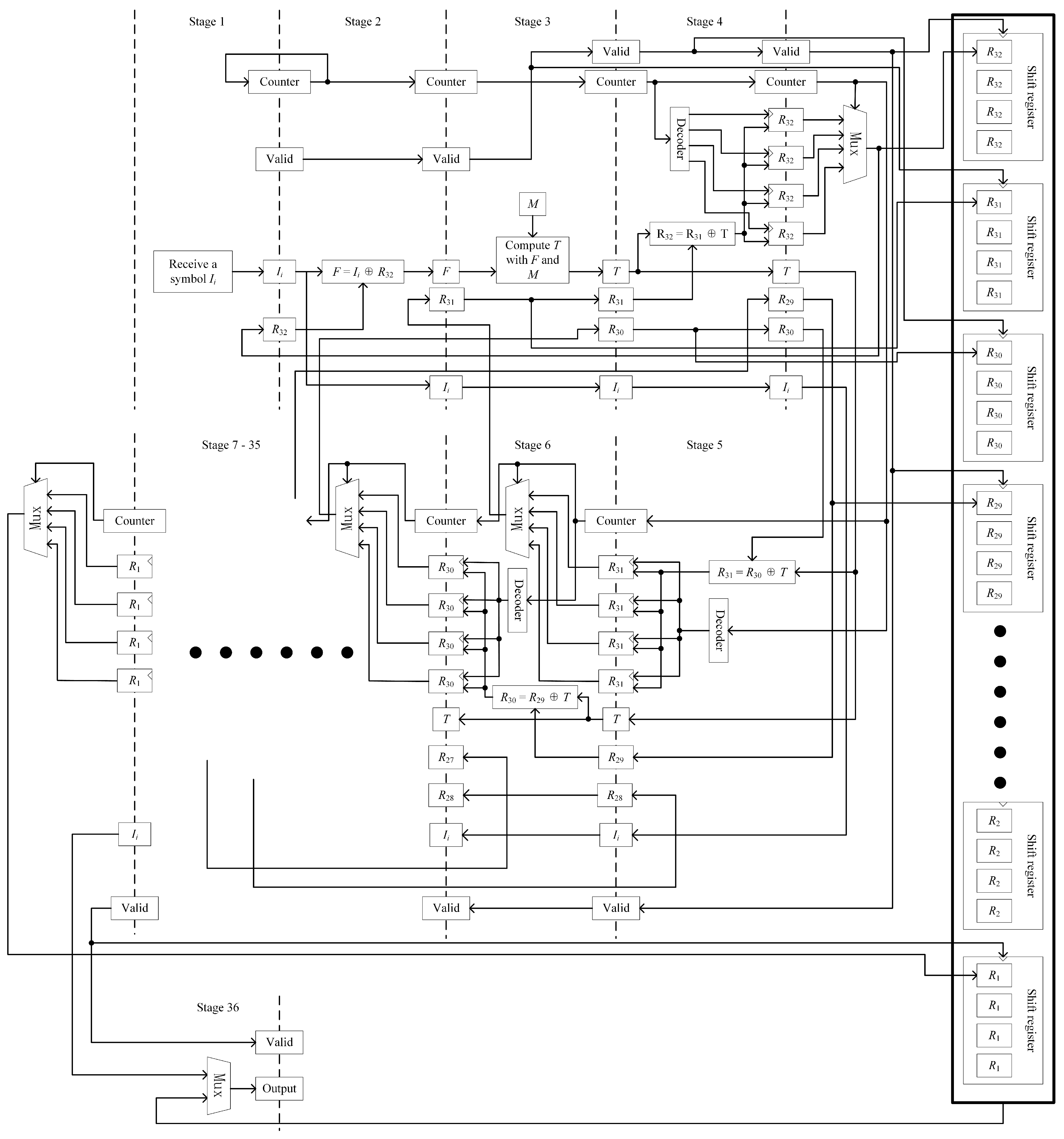
As shown in Figure 3, the interleaved pipelined architecture is proposed. Each segment between two dashed lines in Figure 3 is used to represent a single pipeline stage, with the stage number indicated between the lines. The logic of pipeline stages 1 through 6 and stage 36 is illustrated in detail. The stages from 7 to 35 are implemented by replicating the logic of stage 6 and are represented by ellipses for brevity. This architecture is composed of 36 pipeline stages. In the first stage, the input symbol I j is received. After each symbol is received, a 2-bit counter, which is initialized to zero, is incremented. This counter is used to indicate which of the four error-correcting sequences— I 1 , I 2 , I 3 , or I 4 —the symbol I j belongs to. A 1-bit valid signal is also used. It is initialized to 0 and is set high when a valid symbol is received. Both the valid and counter signals are passed along the pipeline together with the input symbol. At each pipeline stage, the valid signal is checked to determine whether the stage should be activated. Specifically, the registers located along the dashed lines are designated as inter-stage registers, which are used to control the operation of the pipeline. Each stage’s inter-stage register is enabled for writing by the output of the valid register from the preceding stage. When a valid symbol is received, the valid register is set high. This valid signal is successively passed along the pipeline, activating the corresponding inter-stage registers and enabling the pipelined processing of the input data.
The counter is used to determine the interleaved sequence to which the symbol belongs, ensuring that the appropriate inter-stage register group is selected and updated accordingly. Each inter-stage register is composed of four identical sets of parameters, corresponding to the four error-correcting sequences. The counter ensures that data are written to the correct parameter group. An additional register, used for storing the parameter R 32 , is included in the first pipeline stage. This register is updated by the fourth stage and is used in subsequent computations.
In the second stage, parameter F is calculated by performing a bitwise XOR between I i and R 32 . In this stage, the parameter R 32 is supplied from stage 4 and is bypassed through intermediate pipeline stages to reach the current stage. In addition to being used in the computation, I i is also written into the inter-stage register of the subsequent pipeline stage for further propagation.
In the third stage, parameter T is computed according to Equation (9). Within this stage, the parameter matrix M, which stores a set of constants, is utilized. The parameter R 32 is bypassed through this stage and forwarded to the next pipeline stage. Beginning from the third stage, the valid signal is not only used as the write-enable signal for the inter-stage registers but is also employed as both the shift and write-enable control signal for the shift registers.
From stage 4 to stage 35, the parameters R are updated sequentially, with one parameter updated per stage in reverse index order. This staged distribution is intentionally designed to facilitate a narrow and elongated physical layout during hardware placement and routing. By structuring the pipeline in this way, several advantages are realized. First, the routing complexity is significantly reduced. Since each stage handles a smaller, isolated portion of the logic, shorter and more localized signal paths can be achieved. This minimizes the need for long interconnects across wide areas of the chip, which often lead to increased delays and timing violations in dense designs. Second, the narrow geometry allows for easier replication of the encoder module in systems requiring parallel processing. When multiple encoder instances are placed side by side, the elongated structure ensures that horizontal wiring between shared control signals, inputs, and outputs remains manageable. As a result, the design is better suited for high-throughput applications that require wide-bit or multi-channel parallelism.
From stage 4 to stage 35, the parameters R i ( i = 1 to 32) in the parameter matrix R are updated sequentially, with one parameter updated at each stage. Identical logic is applied across all stages. Initially, all parameters in matrix R are set to zero. In each stage, the updated value of R i is computed by performing a bitwise XOR operation between T and R i 1 . Following each update, a 2-to-4 decoder is employed to generate four write-enable signals based on the value of a 2-bit counter. The 2-bit input signal is translated into a 4-bit one-hot output, in which exactly one bit is high, while the others remain low. This one-hot encoding feature enables the 2-bit counter to control four register write-enable signals. Each state of the counter activates the corresponding register, allowing the computed result to be stored separately for the four interleaved error-correcting sequences. The appropriate parameter register is selected based on the current counter value, and the updated result is written accordingly. This mechanism ensures that the results for all four sequences are correctly maintained in parallel throughout the pipeline.
In stage 5, once R 32 has been updated, a 4-to-1 multiplexer (Mux) is employed to select one of the four outputs corresponding to the four interleaved error-correcting sequences. This multiplexer receives four candidate values as inputs, each representing the most recent result of R 32 from one of the sequences. The selection signal is provided by the 2-bit counter, which determines the currently active sequence. Based on the counter value, one of the four inputs is routed through the multiplexer to the output. The selected value is then fed back to stage 1, where it is used in the encoding of the next input symbol that belongs to the same error-correcting sequence. At the same time, the selected value is written into a shift register specifically associated with R 32 . After each write operation, the shift register is shifted by one symbol width to accommodate the next value. Once 892 shifts have been performed—corresponding to the total number of input symbols—the final computed values for all four sequences are retained within the shift register, completing the encoding process.
A similar procedure is followed for the remaining parameters R 31 through R 1 . After each parameter R i is updated in stage n, the value is written into the designated register using the decoder. In stage n + 1 , the value is passed through a Mux and routed to stage n 4 , where it is used for the next symbol encoding. In stage n 3 , the value is written into its corresponding shift register. In stage 36, the final parameter R 1 is selected via a Mux and written directly into its shift register. As long as the number of processed symbols does not exceed 892, the input symbols I i are output directly. Once all 892 symbols have been output, the contents of the 32 shift registers, comprising 128 parameters, are sequentially output. The 32 shift registers are interconnected as a unified structure. During the parameter update phase, shift operations are performed independently within each register. However, during the output phase, all shift registers are treated as a single logical unit. A unified shift is performed across all registers, shifting by one symbol width per clock cycle. This ensures that all encoded parameters are output sequentially and in the correct order.
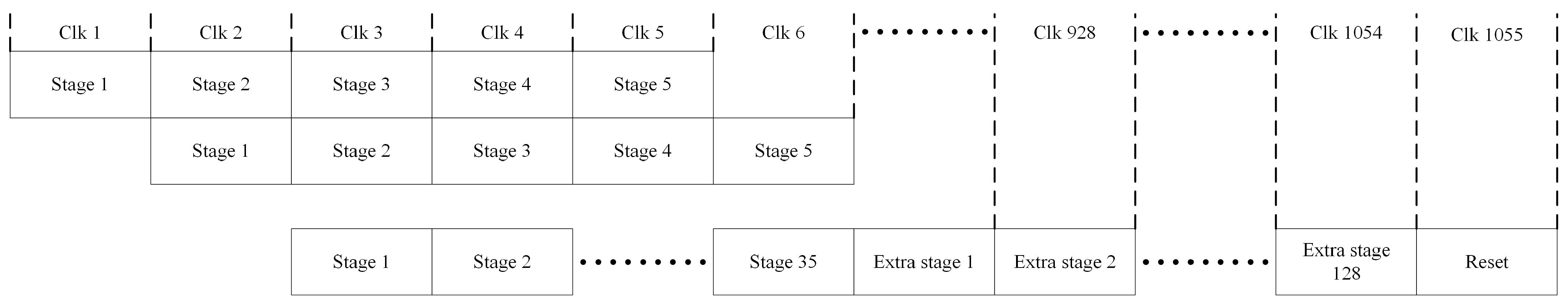
Figure 4 illustrates the operational timing of the pipeline. During the first 892 clock cycles, one symbol is input at each cycle. A total of 892 symbols are processed, corresponding to four interleaved error-correcting sequences, with 223 symbols assigned to each sequence. Each input symbol is propagated through the pipeline and is output 35 clock cycles after it is received.
Once the final input symbol has exited the pipeline, 128 parity symbols are output sequentially. The “extra stage” shown in the figure refers to the stages responsible for outputting these parity symbols, which are generated from the shift operations performed by the 32 shift registers included in the architecture.
Following the completion of parity output, a one-cycle reset is performed to return all pipeline registers to their initial states, preparing the system for the next encoding operation. Including this reset cycle, the total number of clock cycles required to complete the encoding of one full data group 892 symbols is 1055.
Assuming an 8-bit symbol width and an operating frequency of 450 MHz, the theoretical throughput can be calculated as
892 × 8 bits 1055 cycles × 450 MHz 3.043 Gbps
This value reflects the maximum effective throughput of the pipeline, taking into account the one-cycle reset. In practice, the reset operation requires four clock cycles to complete. In the first cycle, stage 1 to stage 5 and the shift registers from R 32 to R 23 are reset. In the second cycle, stage 6 to stage 16 and the shift registers from R 22 to R 13 are reset. In the third cycle, stage 17 to stage 25 and the shift registers from R 12 to R 4 are reset. Finally, in the fourth cycle, stage 26 to stage 36 and the shift registers from R 3 to R 1 are reset. Although the reset process spans four clock cycles, only the first cycle impacts the pipeline data processing. As soon as the first reset cycle is completed, the pipeline is ready to receive new data. Therefore, only one clock cycle is effectively counted toward the reset in the throughput calculation.

4. Validation and Analysis

The RS(255,223) encoder based on the proposed interleaved pipelined architecture was implemented using the Xilinx XC7K325TFFG900-2 FPGA [27]. This device features 203,800 lookup tables (LUTs), 407,600 flip-flops, and 19.16 Mb of block RAM (BRAM). The validation and analysis are focused on two key aspects: the system’s bit flip recovery capabilities and its overall performance.

4.1. Bit Flip Recovery Capabilities

Bit flips can occur in two forms: single-bit upsets (SBUs) and multi-bit upsets (MBUs). SBUs are observed at a much higher frequency than MBUs. RS coding is known to effectively prevent errors caused by SBUs. However, MBUs present a more complex challenge. Under different radiation intensities, various flip patterns can be observed [28,29,30]. A single-event upset that causes two consecutive bits to flip is classified as a double-bit upset (DBU). Similarly, when three consecutive bits flip, it is defined as a triple-bit upset (TBU); four consecutive flips result in a quadruple-bit upset (QDBU); and five consecutive flips are referred to as a quintuple-bit upset (QTBU). Other potential patterns exist but are considered negligible based on empirical observations.
In Figure 5, a representative data pattern stored in flash memory is presented. The red-marked section indicates an MBU—specifically, the most severe case of a QTBU. In this instance, three bit flips occurred in the third error-correcting sequence, resulting in two symbol errors. Meanwhile, two bit flips were observed in the fourth sequences, each also resulting in two symbol errors. Since RS(255,223) is capable of correcting up to 16 symbol errors, each sequence was able to correct its respective errors successfully. This scenario represents the most extreme case.
In the proposed design, the interleaved pipelined architecture ensures that the distance between two adjacent symbols in the same error-correcting sequence is at least three symbol periods. As a result, if any of the specified upset patterns occur, the erroneous symbols are distributed across different sequences. At most, one symbol error occurs per sequence, keeping the errors within the correction capability of each RS code. A single RS(255,223) code is capable of correcting up to 16 symbol errors. By interleaving four such error-correcting sequences, an error correction block is formed. This block can correct up to 64 consecutive errors. Even when spatially consecutive MBU events are present, data integrity can still be maintained by the proposed design.
To verify the system’s recovery capability against bit flips, an error injection method was employed. A set of correct data was generated and written to the flash memory. Errors were then injected externally using debugging techniques. The corrupted data were subsequently read out and corrected. A comparison was made between the corrected output and the originally written data. If the data matched, it was concluded that the proposed architecture successfully mitigated the injected errors. The experimental results confirmed that all injected error patterns were fully corrected, verifying the system’s robustness against both single-bit and multi-bit upsets.

4.2. Performance Evaluation

Evaluating the performance of a single module alone cannot accurately reflect its operating frequency within a complete O-SSR system. This is because the frequency is affected by the overall resource utilization on the FPGA. A single module requires only minimal resources, and this abundance may lead to an unrealistically high operating frequency. To obtain a more realistic assessment, the module was instantiated within a complete O-SSR system. Its resource utilization and operating frequency were then measured under actual operating conditions. The proposed architecture utilized 1728 slice LUTs—324 as memory and 1404 as logic—and a total of 7064 slice Registers. No additional FPGA resources were used. A clock frequency of 450 MHz was achieved by this architecture after applying triple modular redundancy (TMR).
To further highlight the advantages of the proposed architecture in terms of particle-induced bit flip resistance and encoding efficiency, a comprehensive comparison with several recently proposed schemes is presented in Table 1. The selected comparison schemes were all implemented within the O-SSR system or systems with similar architectures. Evaluations were based on three key metrics: the operating frequency, throughput, and radiation resistance capability. The encoding efficiency was assessed through the measurement of the operating frequency and throughput, while radiation tolerance was evaluated by examining the types of bit flip patterns that could be corrected.
To ensure fairness and consistency in the throughput comparison, all values reported in Table 1 reflect the performance of a single encoder module. Although it is technically feasible to enhance the effective throughput by replicating the encoder modules in a multi-core architecture, such an approach significantly increases the resource consumption and can artificially inflate the throughput figures. Therefore, throughput results derived from multi-core replication were deliberately excluded from our analysis. This methodology enabled a more accurate and meaningful assessment of the architectural merits of each design, free from the confounding effects of hardware scaling.
The proposed system achieved operating frequencies that were 3.60 to 4.50 times higher than those of all other schemes, with the exception of [18], with the throughput improved by factors ranging from 2.66 to 17.88. Additionally, the highest level of radiation tolerance was achieved. In contrast, works such as [31,32] employed only Hamming code-based methods, resulting in limited radiation resistance. The approach in [25] combined RS codes with LDPC codes but was only capable of mitigating DBU events. In [33], two different radiation-hardening strategies were selectively applied based on data criticality, where most data were only protected against SBU events, and a small portion of critical data were protected against MBUs. In [20], a strategy was introduced in which data from the same parity sequence were distributed across different memory regions, effectively preventing all DBU events. Meanwhile, [34] proposed an iterative interleaving method based on LDPC encoding, significantly enhancing the radiation resistance. However, this method led to high resource consumption and reduced throughput due to its computational complexity and iterative decoding process.
When compared to the proposed architecture, the design presented in [18] was found to operate at a clock frequency of 50 MHz lower, but with throughput that was 0.06 Gbps higher. This method was also capable of mitigating all SBU events and most MBU events. RS(256,252) codes were employed, and pipelining was utilized to accelerate the RS encoder, enabling operating frequencies and throughput levels comparable to those of the proposed system. Although interleaving techniques were adopted in both schemes, the proposed method integrates interleaving directly into the pipeline, whereas, in [18], a single interleaving module was implemented after the encoder to perform simple post-encoding interleaving.
The slightly lower throughput observed in the proposed system compared to [18] can be attributed to the adoption of a more complex encoding algorithm, RS(255,223), which necessitated the generation of 32 parity symbols per codeword. In contrast, only four parity symbols were required in their RS(256,252) scheme. This variation in algorithm complexity also led to differences in error correction capabilities. While both designs were capable of mitigating most MBU events, the maximum number of correctable errors differed substantially. In the worst-case scenario, up to 64 consecutive erroneous symbols could be corrected by the proposed method, whereas the method in [18] was limited to correcting only eight such symbols.
To account for the influence of the device technology on the performance, a new implementation of the proposed encoder was carried out on the XC4VSX55 platform 90 nm process [35]. This allowed for a direct comparison with earlier architectures implemented on platforms such as M2S150TS and 5CGXFC7D7F31C8, which utilize similar process technologies. It was observed that, even on this legacy device, the proposed architecture maintained superior throughput and radiation tolerance compared to prior methods. This demonstrates that the reported performance benefits are not solely the result of advanced hardware but are attributable to the underlying architectural enhancements.

5. Conclusions

The interleaved pipelined architecture proposed in this study is designed to effectively address the challenges associated with deploying the RS(255,223) encoder. The serial implementation of RS(255,223) has been constrained by its inherent algorithmic structure, which limits the depth of pipelining that can be achieved. These issues are mainly caused by long dependency chains between computation parameters. Parallel implementations, on the other hand, have been hindered by resource inefficiencies.
To overcome these constraints, an interleaving technique was incorporated into the pipelined structure. By enabling the encoder to alternate among four parity codewords, a four-cycle latency window was created for parameters with interdependencies. Consequently, a 36-stage pipeline was implemented. Through this design, a substantial increase in throughput was achieved, allowing performance levels that typically require extensive parallelism to be reached with significantly reduced parallel scaling. Additionally, the introduction of interleaving was found to inherently enhance the system’s radiation tolerance.
The proposed architecture was thoroughly evaluated on the Xilinx XC7K325T platform, with specific attention given to throughput and error correction capabilities. It was analytically and experimentally verified that the system was capable of correcting all classified error types, demonstrating its effectiveness in recovering from both SBUs and MBUs. The results confirmed that high data rates can be supported while maintaining strong error correction performance. Although the achieved throughput was found to be slightly lower than that of the most advanced existing solution, a significantly higher level of radiation tolerance was demonstrated. As such, the proposed architecture is considered well suited for future deployment in space exploration missions where both high throughput and robust radiation resistance are critical.
The design was validated through extensive error injection experiments, which confirmed its resilience against a variety of bit flip patterns. However, it should be acknowledged that the radiation resilience was evaluated using fault injection, which serves as an indirect method of validation. Real-space or radiation chamber testing was not conducted in this study. As such, future work will include physical radiation testing to further substantiate the fault-tolerant capabilities of the proposed architecture under actual space or radiation-rich conditions. This step is expected to enhance the credibility and applicability of the design for space-grade and safety-critical systems.
While the current evaluation was conducted on a single module, potential scalability in system-level integration scenarios has also been taken into account. Due to its modular and pipelined structure, the proposed architecture is considered inherently suitable for deployment in multi-core encoder systems. Under high-traffic conditions, multiple encoder instances may be instantiated and operated in parallel, with efficiency maintained through appropriate scheduling and load-balancing mechanisms. Nonetheless, scalability challenges, such as interconnect bottlenecks and shared resource contention, may be encountered and will need to be carefully addressed in future multi-core system implementations. In future work, these multi-encoder configurations will be explored in greater depth, with the goal of optimizing the encoder performance in large-scale, high-throughput applications.

Author Contributions

Software, X.L.; validation, X.L.; formal analysis, X.L.; investigation, X.L.; writing—original draft, X.L.; writing—review and editing, X.L. and L.Z.; supervision, L.Z.; project administration, X.L.; funding acquisition, Y.Z. All authors have read and agreed to the published version of the manuscript.

Funding

This research was funded by the Science Foundation of the Chinese Academy of Sciences, grant number E4GZ120503.

Data Availability Statement

The raw data supporting the conclusions of this article will be made available by the authors on request.

Conflicts of Interest

The authors declare no conflicts of interest.

References

  1. Song, Q.; Li, S.; Zhu, Y.; An, J.S. Design and Research of Multiple Data Channels in Solid State Recorder of the Satellite SJ-10. Adv. Mater. Res. 2015, 1073, 1977–1981. [Google Scholar] [CrossRef]
  2. Fabiano, M.; Furano, G. NAND flash storage technology for mission-critical space applications. IEEE Aerosp. Electron. Syst. Mag. 2013, 28, 30–36. [Google Scholar] [CrossRef]
  3. Khaled, A.; Zhang, Q. An Energy Aware Mass Memory Unit for Small Satellites Using Hybrid Architecture. In Proceedings of the 2017 IEEE International Conference on Computational Science and Engineering (CSE) and IEEE International Conference on Embedded and Ubiquitous Computing (EUC), Guangzhou, China, 21–24 July 2017; Volume 1, pp. 210–213. [Google Scholar] [CrossRef]
  4. Tu, S.; Wang, H.; Huang, Y.; Jin, Z. A spaceborne advanced storage system for remote sensing microsatellites. Front. Inf. Technol. Electron. Eng. 2024, 25, 600–615. [Google Scholar] [CrossRef]
  5. Höeffgen, S.K.; Metzger, S.; Steffens, M. Investigating the effects of cosmic rays on space electronics. Front. Phys. 2020, 8, 318. [Google Scholar] [CrossRef]
  6. Li, X.; Wen, X.; Xiong, S.; An, Z.; Xu, Y.; Liang, X.; Liu, X.; Yang, S.; Zhang, F.; Sun, X.; et al. Introduction to the SATech-01 satellite HEBS (GECAM-C). Exp. Astron. 2025, 59, 1–22. [Google Scholar] [CrossRef]
  7. Jia, S.m.; Song, L.m.; Li, C.k.; Zhao, H.S.; Zhang, J.; Guan, J.; Ou, G.; Wang, J. The operation and data processing of the Einstein Probe FXT science data center. In Radiation Detection Technology and Methods; Springer: Berlin/Heidelberg, Germany, 2025; pp. 1–7. [Google Scholar]
  8. Tian, S.; Li, C.; Zhao, L.; Yan, G.; Luo, W.; Gao, Y. Information Processing Technology of Housekeeping Subsystem for BJ-3A/B Satellites. Spacecr. Eng. 2023, 32, 85–92. [Google Scholar]
  9. Ribet, M.; Sabatini, M.; Lampani, L.; Gasbarri, P. Monitoring of a controlled space flexible multibody by means of embedded piezoelectric sensors and cameras synergy. J. Intell. Mater. Syst. Struct. 2018, 29, 2966–2978. [Google Scholar] [CrossRef]
  10. Aritome, S. NAND Flash Memory Technologies; John Wiley & Sons: New York, NY, USA, 2015. [Google Scholar]
  11. Open NAND Flash Interface Workgroup. Open NAND Flash Interface Specification, 5.1 ed.; Open NAND Flash Interface Workgroup: Arlington, VA, USA, 2022. [Google Scholar]
  12. Gonzales, L.; Danzeca, S.; Fiore, S.; Kramberger, I. Mixed-Field Radiation of 3-D MLC Flash Memories for Space Applications. IEEE Trans. Nucl. Sci. 2024, 71, 2400–2408. [Google Scholar] [CrossRef]
  13. Peterson, W.W.; Weldon, E.J. Error-Correcting Codes, 2nd ed.; MIT Press: Cambridge, MA, USA, 1972. [Google Scholar]
  14. Garg, D.; Sharma, C.P.; Chaurasia, P.; Chowdhury, A.R. High throughput FPGA implementation of Reed-Solomon Encoder for Space Data Systems. In Proceedings of the 2013 Nirma University International Conference on Engineering (NUiCONE), Ahmedabad, India, 28–30 November 2013; pp. 1–5. [Google Scholar] [CrossRef]
  15. Samanta, J.; Bhaumik, J.; Barman, S. FPGA based area efficient RS (23, 17) codec. Microsyst. Technol. 2017, 23, 639–650. [Google Scholar] [CrossRef]
  16. Rurik, W.; Mazumdar, A. Hamming codes as error-reducing codes. In Proceedings of the 2016 IEEE Information Theory Workshop (ITW), Cambridge, UK, 11–14 September 2016; pp. 404–408. [Google Scholar] [CrossRef]
  17. Ge, G.; Yin, L. LDPC coding scheme for improving the reliability of multi-level-cell NAND flash memory in radiation environments. China Commun. 2017, 14, 10–21. [Google Scholar] [CrossRef]
  18. Li, X.; Zhou, L.; Zhu, Y. A Novel Architecture for Addressing the Throughput Bottleneck in Spaceborne Solid-State Recorder for Electromagnetic Spectrum Sensors. Remote Sens. 2025, 17, 138. [Google Scholar] [CrossRef]
  19. Silva, M.G.; Silvano, G.L.; Duarte, R.O. RTL development of a parameterizable Reed–Solomon Codec. IET Comput. Digit. Tech. 2021, 15, 143–159. [Google Scholar] [CrossRef]
  20. Zhang, X. Research of High Speed Synchronous NAND FLASH Spaceborne Storage Technology. Master’s Thesis, University of Chinese Academy of Sciences (National Space Science Center of Chinese Academy of Sciences), Beijing, China, 2020. [Google Scholar]
  21. Bartz, H.; Puchinger, S. Fast decoding of lifted interleaved linearized Reed–Solomon codes for multishot network coding. Des. Codes Cryptogr. 2024, 92, 2379–2421. [Google Scholar] [CrossRef]
  22. Gil-Tomás, D.; Saiz-Adalid, L.J.; Gracia-Morán, J.; Carlos Baraza-Calvo, J.; Gil-Vicente, P.J. A Hybrid Technique Based on ECC and Hardened Cells for Tolerating Random Multiple-Bit Upsets in SRAM Arrays. IEEE Access 2024, 12, 70662–70675. [Google Scholar] [CrossRef]
  23. Geisel, W.A. Tutorial on Reed-Solomon Error Correction Coding; National Aeronautics and Space Administration, Lyndon B. Johnson Space Center: Houston, TX, USA, 1990; Volume 102162. [Google Scholar]
  24. Wolf, J.K. An introduction to Reed-Solomon Codes. Course Notes. 2020. Available online: http://pfister.ee.duke.edu/courses/ecen604/rspoly.pdf (accessed on 4 January 2021).
  25. Xu, Z. Research on Solid-State Storage Technology for Spaceborne Integrated Electronic Systems. Ph.D. Thesis, University of Chinese Academy of Sciences (National Space Science Center, Chinese Academy of Sciences), Beijing, China, 2017. [Google Scholar]
  26. Dayal, P.; Patial, R.K. Implementation of Reed-Solomon CODEC for IEEE 802.16 network using VHDL code. In Proceedings of the 2014 International Conference on Reliability Optimization and Information Technology (ICROIT), Faridabad, India, 6–8 February 2014; pp. 452–455. [Google Scholar] [CrossRef]
  27. Xilinx. Kintex-7 FPGAs Data Sheet(DS182), 2.17 ed.; Xilinx: San Jose, CA, USA, 2019. [Google Scholar]
  28. Radaelli, D.; Puchner, H.; Wong, S.; Daniel, S. Investigation of multi-bit upsets in a 150 nm technology SRAM device. IEEE Trans. Nucl. Sci. 2005, 52, 2433–2437. [Google Scholar] [CrossRef]
  29. Zhang, Z.; Liu, J.; Hou, M.; Sun, Y.; Hong, S.U.; Geng, C.; Yao, H.; Luo, J.; Duan, J.; Dan, M.O. Investigation of Multiple-bit Upsets in Anisotropic SRAM Device. Nucl. Phys. Rev. 2014, 31, 195–200. [Google Scholar] [CrossRef]
  30. Chabot, A.; Alouani, I.; Niar, S.; Nouacer, R. A New Memory Reliability Technique for MULTIPLE Bit Upsets Mitigation. In Proceedings of the 16th ACM International Conference on Computing Frontiers, Alghero, Italy, 30 April–2 May 2019; pp. 145–152. [Google Scholar] [CrossRef]
  31. Zhongjie, W. Research of On-board Data Routing Multiplexing and Storage. Master’s Thesis, Harbin Institute of Technology, Harbin, China, 2016. [Google Scholar]
  32. Pan, L. Research of Key Technologies of Onboard Mass Storage Base Done MMC. Master’s Thesis, Harbin Institute of Technology, Harbin, China, 2017. [Google Scholar]
  33. Qingan, L. Virtual Multichannel Storage Technology for Large Capacity Spaceborne Data. Master’s Thesis, Huazhong University of Science and Technology, Wuhan, China, 2019. [Google Scholar]
  34. Hao, Z. Research on LDPC Coding and Onboard Multi-Channel Storage System. Master’s Thesis, Hunan University of Technology, Zhuzhou, China, 2024. [Google Scholar] [CrossRef]
  35. Xilinx. Virtex-4 Family Overview(DS112), 3.1 ed.; Xilinx: San Jose, CA, USA, 2010. [Google Scholar]
Figure 1. Example of widely adopted RS(255,223) hardware architecture. This figure illustrates the operational flow of a traditional architecture.
Electronics 14 02447 g001
Figure 2. Interleaved distribution of output symbols in the proposed RS(255,223) encoder. A total of 892 input symbols are divided into four interleaved sequences, each assigned a distinct color corresponding to separate error-correcting codewords.
Electronics 14 02447 g002
Figure 3. Implementation of the RS(255,223) algorithm in a interleaved pipelined architecture. A detailed view of the 36-stage pipeline structure is shown in this figure.
Electronics 14 02447 g003
Figure 4. Timing diagram illustrating the processing and output of the interleaved pipelined architecture.
Electronics 14 02447 g004
Figure 5. Flash memory data pattern with the red highlighted region indicating a severe QTBU case.
Electronics 14 02447 g005
Table 1. A comparison between the existing architectures and our proposed architecture. SBU: Single-Bit Upset, MBU: Multi-Bit Upset, DBU: Double-Bit Upset.
ArchitectureTechnologyFrequencyThroughputRadiation ResistanceYear
 [31]M2S150TS100 MHz0.32 GbpsAll SBU2017
[25]XC4VSX55100 MHz0.42 GbpsAll SBU and Limited DBU2017
[32]5CGXFC7D7F31C8120 MHz0.17 GbpsAll SBU2018
[33]XC5VLX330100 MHz0.30 GbpsAll SBU and Limited MBU2020
[20]M2S150TS125 MHz0.80 GbpsAll SBU and All DBU2021
[34]XC5VFX130T100 MHz1.14 GbpsAll SBU and Most MBU2024
[18]XC7K325T400 MHz3.10 GbpsAll SBU and Most MBU2024
ProposedXC7K325T450 MHz3.04 GbpsAll SBU and Most MBU2025
XC4VSX55290 MHz1.95 Gbps
Disclaimer/Publisher’s Note: The statements, opinions and data contained in all publications are solely those of the individual author(s) and contributor(s) and not of MDPI and/or the editor(s). MDPI and/or the editor(s) disclaim responsibility for any injury to people or property resulting from any ideas, methods, instructions or products referred to in the content.

