1. Introduction
Flat panel display technology has changed from voltage-driven liquid crystal displays (LCDs) in the 1990s to current-driven organic light emitting diodes (OLEDs) in the 2000s [
1,
2,
3,
4,
5,
6,
7,
8,
9,
10,
11,
12,
13]. For reference, voltage-driven LCDs mean that the brightness of LCDs is controlled by the delta voltage between positive and negative electrodes, and current-driven OLEDs mean that the brightness of OLEDs is controlled by the OLED current of the driving transistor, which supplies current from ELVDD to OLED. In order to supply a constant current to each pixel of the panel, it is important to supply the power signal evenly within the panel from the aspect of panel design. Therefore, a relatively large power line design with thick line width and metal thickness is inevitably required. As the panel size moves beyond the monitor to home applications, the power line design is also bound to grow. Due to this structural vulnerability, particles generated in the manufacturing process have become a key item in yield improvement activities.
During mass production, rapid yield ramp-up is key to high profits early in the product’s lifetime. Therefore, we set the target yield at an extreme value, over the golden yield (90%). Generally, the main factors affecting yield loss, lifted insulators, and etched active pattern defects need to be improved to meet this extreme target yield.
Previous methods of reducing process particles have been to develop equipment and add one process to the manufacturing process: (1) Developing sputtering targets (rotation target arrays) that provide less material redeposition and nodule formation, gradually reducing the number of particles, improving device performance, yield, and product value [
14]. (2) The sacrificial layers that operated to reduce panel failures due to particles [
15]. However, such cases require huge investment and additional layers in the equipment and take a long time to set up the equipment and build new processes. Otherwise, design changes for mitigation are relatively inexpensive, fast, and have a better impact on reducing defect rates.
In this paper, we focused on defining the root causes of “lifted insulator and etched active pattern defects” and providing a new design with a large power line to prevent defects in advance. For reference, large power lines are composed of an ELVDD, supplying high (positive) voltages to the panel, and an ELVSS, providing low (negative) voltages.
2. Results and Discussion
2.1. Phenomenon Analysis
A lifted insulator (SiOx) defect is circular and has a submicron particle at its center (
Figure 1a). An active (Indium Gallium Zinc Oxide, IGZO) pattern defect is etched starting from a lifted insulator defect, especially from a submicron defect (
Figure 1b). One can say that a submicron defect is the origin of both of these defects. An etched active pattern defect makes the source–drain pattern of the driving transistor open or thinning so that an on-state dark dot occurs in a display panel due to decreased current from the driving transistor.
2.2. Step-by-Step Defect Review to Search for the Processes That Cause These Defects
To determine the processes in which defects occur, we adopted a step trace method that reviews defects on the glass right after each process with optical inspection equipment. We made three conclusions: (1) a submicron defect occurs in a particle before or during insulator deposition (no defect before insulator deposition and defects were found right after insulator deposition); (2) a lifted insulator defect is generated after insulator deposition but during active deposition (no defect before active deposition and defects were found right after active deposition); and (3) an etched active pattern defect is generated during the active chemical wet etch process (no defect before active chemical wet etch process and defects were found right after active chemical wet etch process).
Figure 1.
(a) A submicron particle on the large power line that is metal 1, Cu in the top view, (b) the insulator lifted at the center of a submicron particle (vertical view), (c) active pattern in driving transistor, and (d) etched active pattern (source–drain open).
Figure 1.
(a) A submicron particle on the large power line that is metal 1, Cu in the top view, (b) the insulator lifted at the center of a submicron particle (vertical view), (c) active pattern in driving transistor, and (d) etched active pattern (source–drain open).
2.3. Process Condition Changing Test
After we changed the active material from IGZO to the transparent conductive oxide (TCO, Indium Tin Oxide), etched pattern defects were not found in any part of the glass because ITO deposition gas has no H
2O, including OH- having weaker bonding energy than that of O
2 in ITO deposition. It means that the active deposition gas causes defects. Decreasing the flow rate of the suspicious gas (oxygen in H
2O) to zero during active deposition reduced the lifted insulator defect rate to zero (no defect in dozens of glasses). Additionally, conditions decreasing the deposition time reduced the number of defects. Therefore, the reaction that creates these defects occurs at the beginning of IGZO deposition. In summary, lifted insulator defects are generated during active deposition due to one of the deposition gases (
Table 1).
Additionally, we determined the relation between lifted insulators and etched active pattern defects.
2.4. Defect Generation Mechanism
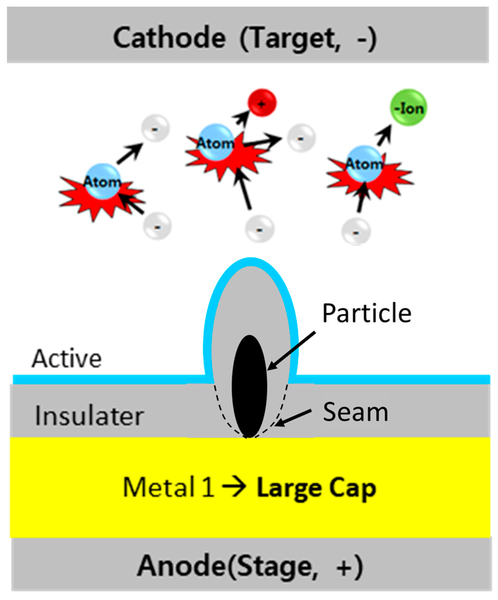
Based on a step-by-step defect review, we could infer the relation between lifted insulators and etched active pattern defects. First, a submicron particle from the equipment of insulator deposition was dropped on metal 1 before insulator deposition and covered with an insulator that has a weak step coverage around submicron particles due to its intrinsic chemical vapor deposition (CVD) film growth characteristics (
Figure 2): a micro-crack in the insulator is called a “seam”, which is from the columnar grains due to anisotropy in the growth rate of nuclei on the substrate [
16].
- (a)
Lifted Insulator Defects
During active (IGZO) deposition, oxygen (O) dissociates from water vapor (H
2O) in the plasma in the sputtering chamber (Equation (1)). Negatively charged oxygen ions (O-) can result from the ionization of oxygen atoms in the plasma and strike the insulator from the beginning of active deposition because of metal 1 with a positive polarity relatively. These striking supplies bombard energy to the surface of the insulator on the metal and act as a large capacitor attracting negatively charged oxygen ions. The surface temperature of the insulator increased to create the insulating gap in
Figure 1b. This thermal energy was then transferred to the insulator and metal 1, which have different coefficients of thermal expansion (CTEs), as shown in
Table 2. In
Figure 1b, the lifted insulator gap is about 0.2 μm. Since horizontal thermal expansion was reflected in the vertical direction, we could calculate the surface temperature of the insulator during IGZO deposition to be about 630 °C (with a power line width of 20 μm, ΔCTE = 16 μm/m), which is not much different from substrate temperature in [
17]. Additionally, an insulator gap was created at the defect due to the non-continuous surface causing thermal stress concentration. According to the defect generation mechanism, larger power lines attract negative oxygen ions. We propose the design of a new, smaller power line later, as follows:
- (b)
Etched Active Pattern Defects
Phenomenologically, an active pattern was etched starting from a micron particle centered on the lifted insulator and was rapidly etched into a round shape due to electrons lost to metal 1 through micro-cracks during active etching because of the standard electrode potential (SEP) difference between the active pattern (IGZO) and metal 1 (
Table 3). This is a kind of galvanic corrosion due to the micro-scale distance from the lifted insulator defect to the active pattern. Galvanic corrosion can be represented by the galvanic current (I), the integrated current of the cathodic (IGZO) to the anodic (metal 1). Another factor in galvanic corrosion is the large power line area per line (Ap), which attracts negatively charged components from the IGZO to its large capacity (
Figure 2) [
18,
19]. The second factor (the large power line area per line, Ap) is more significant than the first one (I) because Ap determines the amount of current in galvanic corrosion as
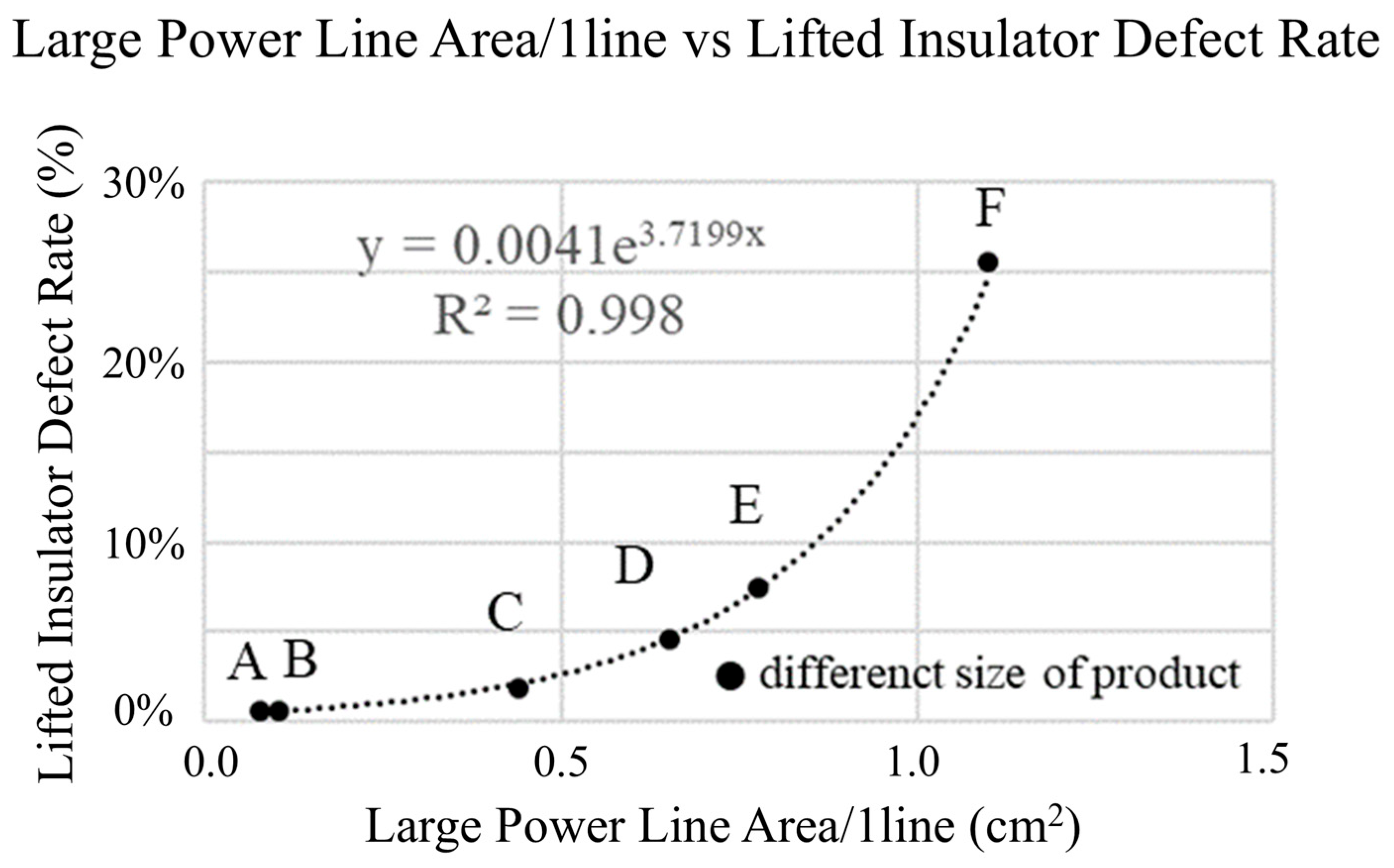
Figure 3.
2.5. Design Modification
The insulator lifting defect rate (the number of defects in one glass/cell number) increases exponentially as the panel size becomes larger. As shown in
Figure 3, the lifted insulator defect rate of the largest panel F decreased to an acceptable rate by downsizing the large power line (C, the separated large power line). The large power line area of panel C is the optimum value (<0.44 cm
2) that can be used to check the design of new products before they are photo-masked with tape. It will be referenced in detail later.
2.6. Design Verification
Before separating the large power lines, we checked the side effects: luminance uniformity, power consumption due to increased line resistance (17% ↑), and image sticking. The luminance uniformity and power consumption were not different from those used in conventional single power line designs (normalized luminance uniformity: Ref. normalized value 1 → separated design 0.996; normalized power consumption: 1 → 1.009). However, image sticking (OLED lifetime) decreased by up to 75% because of the increased resistance (17% ↑) of the separated power line, which decreased the amount of compensated pixel current for a long operation. In the pixel circuit (
Figure 4), the resistance components of the power line were increased, Ra to 2Ra, and Rc was added.
To overcome the increased resistance of power lines, we increased the thickness of metal 1 to reduce the resistance of the separated power line to that of the conventional single power line. The increased thickness of metal 1 had no side effects like the step opening of metal lines on metal 1.
2.7. Design Rule
As mentioned before, we can determine the golden value for large power line areas per line (normalized) to obtain stable yield when manufacturing panels in exponential relation to the lifted insulator defect rate. Additionally, for our next new product, we implemented a rule to check large power lines to prevent lifted insulators and etched active pattern defects based on the line area size and the use of a separated power line for medium-sized panels (that is, larger than panel C). In principle, this design can be applied to every medium-sized panel.
3. Conclusions
Based on a hypothesis from the defect phenomenon analysis, we investigated the mechanism behind lifted insulators and etched active pattern defects through experiments. Moreover, we devised a new design to suppress fundamental occurrences and applied it to mass production. In addition, we found the optimum value (<0.44 cm2) that can be used to check the large power line area per line of new products before fixing the panel design. Through this research, we proposed the mechanism behind defect generation and a novel design rule that can be used for medium-sized home displays.
4. Patents
Patent applications have been submitted in the US, China, and South Korea.
Author Contributions
D.L. defined the problem, analyzed the phenomena, and revised the mitigating design; W.L. revised the mitigating design; J.P. performed the tests and verifications during the fab. process; S.L. designed the separated large power line. B.-K.J. organized all procedures of this study. All authors have read and agreed to the published version of the manuscript.
Funding
This work was supported by an internal project of Samsung Display.
Data Availability Statement
The data presented in this study are confidential. However, we can share specific data with permission from Samsung Display Co.
Acknowledgments
We express our gratitude to our co-authors who actively participated in this project despite their busy schedules. Additionally, we thank our advisor.
Conflicts of Interest
Authors Wonhee Lee, Jongcheol Park and Seongyoung Lee were employed by the company Samsung Display Co., Ltd. The remaining authors declare that the research was conducted in the absence of any commercial or financial relationships that could be construed as a potential conflict of interest.
References
- Display, L.G. OLED Technology Prepares for Landing in the Commercial TV Market. Inf. Disp. 2012, 28, 33–36. [Google Scholar] [CrossRef]
- World’s Largest Oled TV from Lg Offers More Realistic Colors, Brighter Picture, Faster Speed. Available online: www.newswire.co.kr (accessed on 2 January 2012).
- LG bringing OLED TV to CES. Available online: http://variety.com (accessed on 3 January 2012).
- Next Samsung Electronics’ QLED TV’s Name to Be SUHD QLED TV. etnews.com. Retrieved 3 April 2018. Available online: www.etnews.com (accessed on 18 October 2016).
- How QLED TV Could Help Samsung Finally Beat LG’s OLEDs. Retrieved 3 April 2018. Available online: www.cnet.com (accessed on 30 June 2016).
- Chen, J.; Hardev, V.; Yurek, J. Quantum-dot displays: Giving LCDs a competitive edge through color. Inf. Disp. 2013, 29, 12–17. [Google Scholar] [CrossRef]
- Luo, Z.; Xu, D.; Wu, S.-T. Emerging quantum-dots-enhanced LCDs. J. Disp. Technol. 2014, 10, 526–539. [Google Scholar] [CrossRef]
- Li, G.; Tseng, M.-C.; Chen, Y.; Yeung, F.S.-Y.; He, H.; Cheng, Y.; Cai, J.; Chen, E.; Kwok, H.-S. Color-conversion displays: Current status and future outlook. Light. Sci. Appl. 2024, 13, 301. [Google Scholar] [CrossRef] [PubMed]
- Quantum Dots. Available online: https://lateralflows.com/quantum-dots/ (accessed on 10 June 2025).
- Quantum Dots for Electronics and Energy Applications. Available online: www.sigmaaldrich.com (accessed on 10 June 2025).
- Vitukhnovskii, A.G.; Vaschenko, A.A.; Bychkovskii, D.N.; Dirin, D.N.; Tananaev, P.N.; Vakshtein, M.S.; Korzhonov, D.A. Photo-and electroluminescence from semiconductor colloidal quantum dots in organic matrices: QD-OLED. Semiconductors 2013, 47, 1567–1569. [Google Scholar] [CrossRef]
- Palomaki, P. Quantum Dots+ OLED= Your Next TV: Formerly rival technologies will come together in new Samsung displays. IEEE Spectr. 2022, 59, 52–53. [Google Scholar] [CrossRef]
- Park, Y.G.; Cho, D.Y.; Kim, R.; Kim, K.H.; Lee, J.W.; Lee, D.H.; Jeong, S.I.; Ahn, N.R.; Lee, W.G.; Choi, J.B.; et al. Defect Engineering for High Performance and Extremely Reliable a-IGZO Thin-Film Transistor in QD-OLED. Adv. Electron. Mater. 2022, 8, 2101273. [Google Scholar] [CrossRef]
- Cunningham, K.L. A process for using oxide TFTs over LTPS TFTs for OLED-TV manufacturing. Inf. Disp. 2015, 31, 28–33. [Google Scholar] [CrossRef]
- Park, C.I.; Seong, M.; Kim, M.A.; Kim, D.; Jung, H.; Cho, M.; Lee, S.H.; Lee, H.; Min, S.; Kim, J.; et al. World’s first large size 77-inch transparent flexible OLED display. J. Soc. Inf. Disp. 2018, 26, 287–295. [Google Scholar] [CrossRef]
- Carlsson, J.O.; Martin, P.M. Chemical vapor deposition. In Handbook of Deposition Technologies for Films and Coatings; William Andrew Publishing: Norwich, NY, USA, 2010; pp. 314–363. [Google Scholar]
- Rocha-Cuervo, J.J.; Uribe-Lam, E.; Treviño-Quintanilla, C.D.; Melo-Maximo, D.V. Sputtering plasma effect on zinc oxide thin films produced on photopolymer substrates. Polymers 2023, 15, 2283. [Google Scholar] [CrossRef] [PubMed]
- Souto, R.M.; González-García, Y.; Bastos, A.; Simões, A. Investigating corrosion processes in the micrometric range: A SVET study of the galvanic corrosion of zinc coupled with iron. Corros. Sci. 2007, 49, 4568–4580. [Google Scholar] [CrossRef]
- Mansfeld, F.; Kenkel, J.V. Galvanic corrosion of Al alloys—III. The effect of area ratio. Corros. Sci. 1975, 15, 239–250. [Google Scholar] [CrossRef]
| Disclaimer/Publisher’s Note: The statements, opinions and data contained in all publications are solely those of the individual author(s) and contributor(s) and not of MDPI and/or the editor(s). MDPI and/or the editor(s) disclaim responsibility for any injury to people or property resulting from any ideas, methods, instructions or products referred to in the content. |
© 2025 by the authors. Licensee MDPI, Basel, Switzerland. This article is an open access article distributed under the terms and conditions of the Creative Commons Attribution (CC BY) license (https://creativecommons.org/licenses/by/4.0/).


