
A Low-Power 868 MHz BJT-Based LNA with Microstrip Matching for Wake-Up Receivers in IoT Applications


Abstract
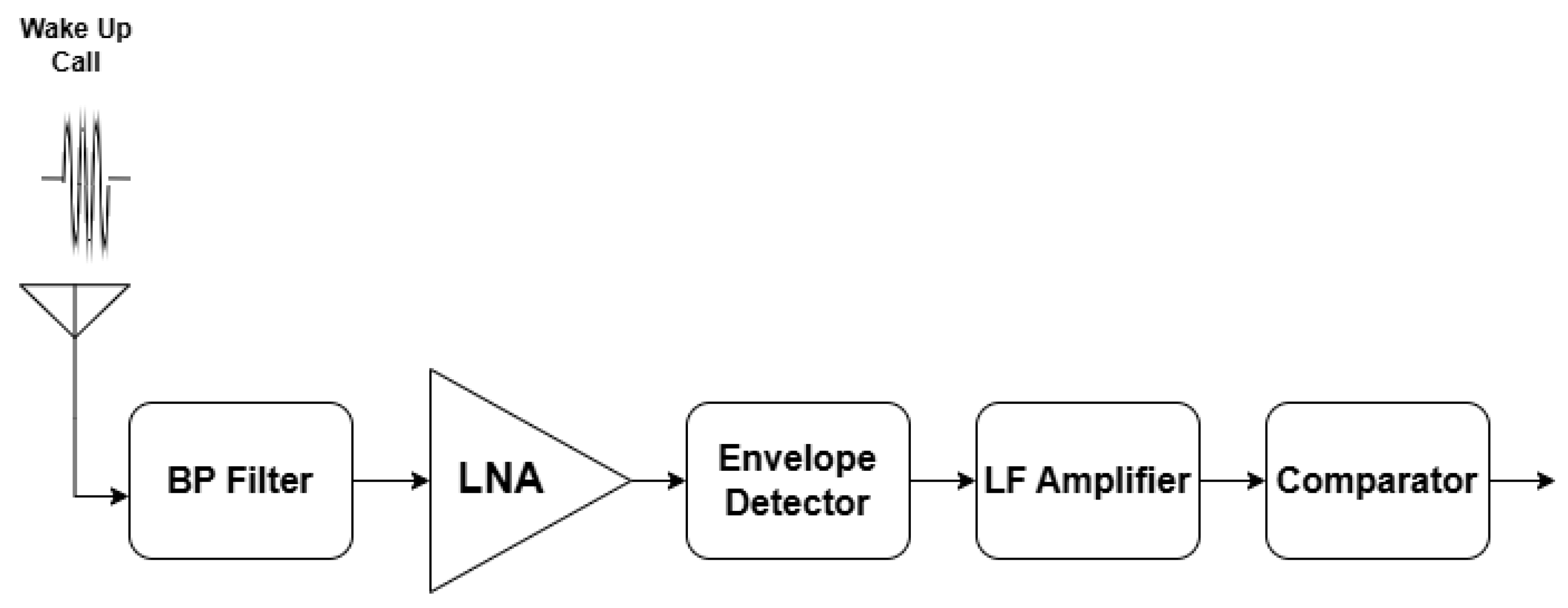
1. Introduction
2. Theoretical Background and State of Research on LNA Design for Wake-Up Receiver Front-End
3. Target Specifications and Design Requirements for Low-Noise Amplifier Implementation
3.1. Transistor Selection Criteria for Low-Noise Amplifier Design
3.2. Gain Metrics in RF Front-End Design: Implications for WuRx Sensitivity
3.3. Stability Considerations in LNA Circuit Design
3.4. Circuit Noise Figure
3.5. Optimizing Gain and Noise Through Bilateral Matching in LNAs
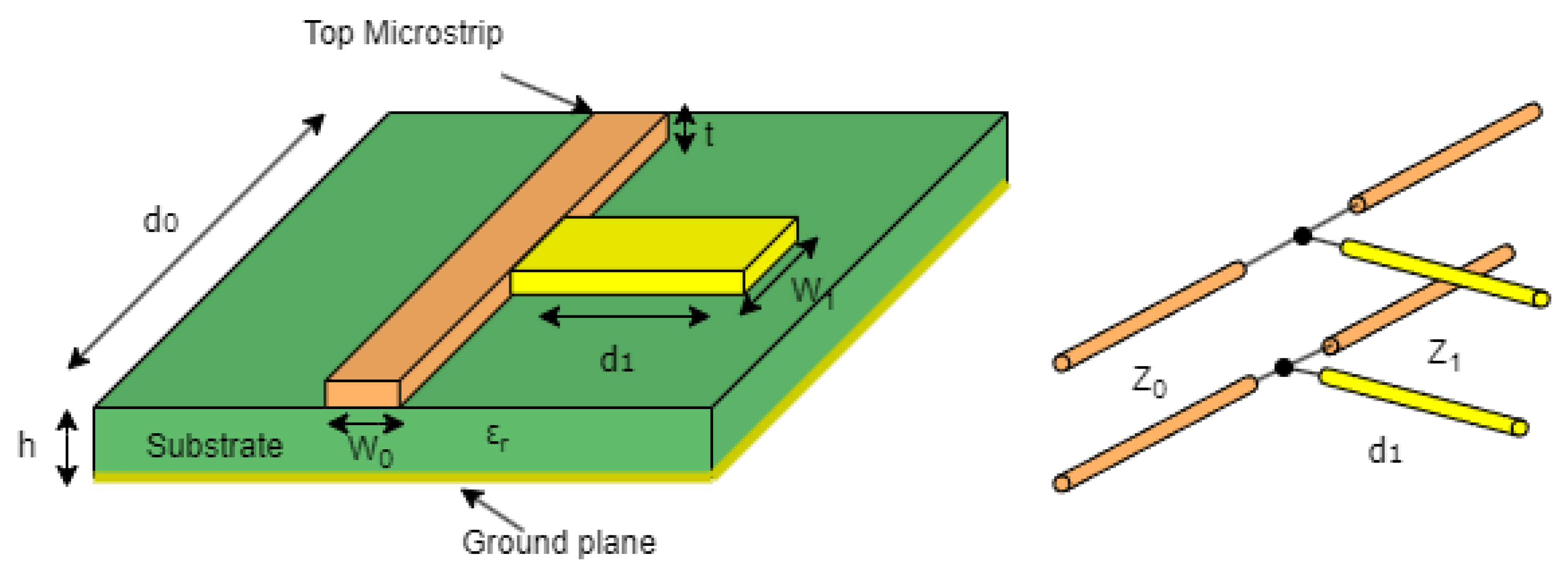
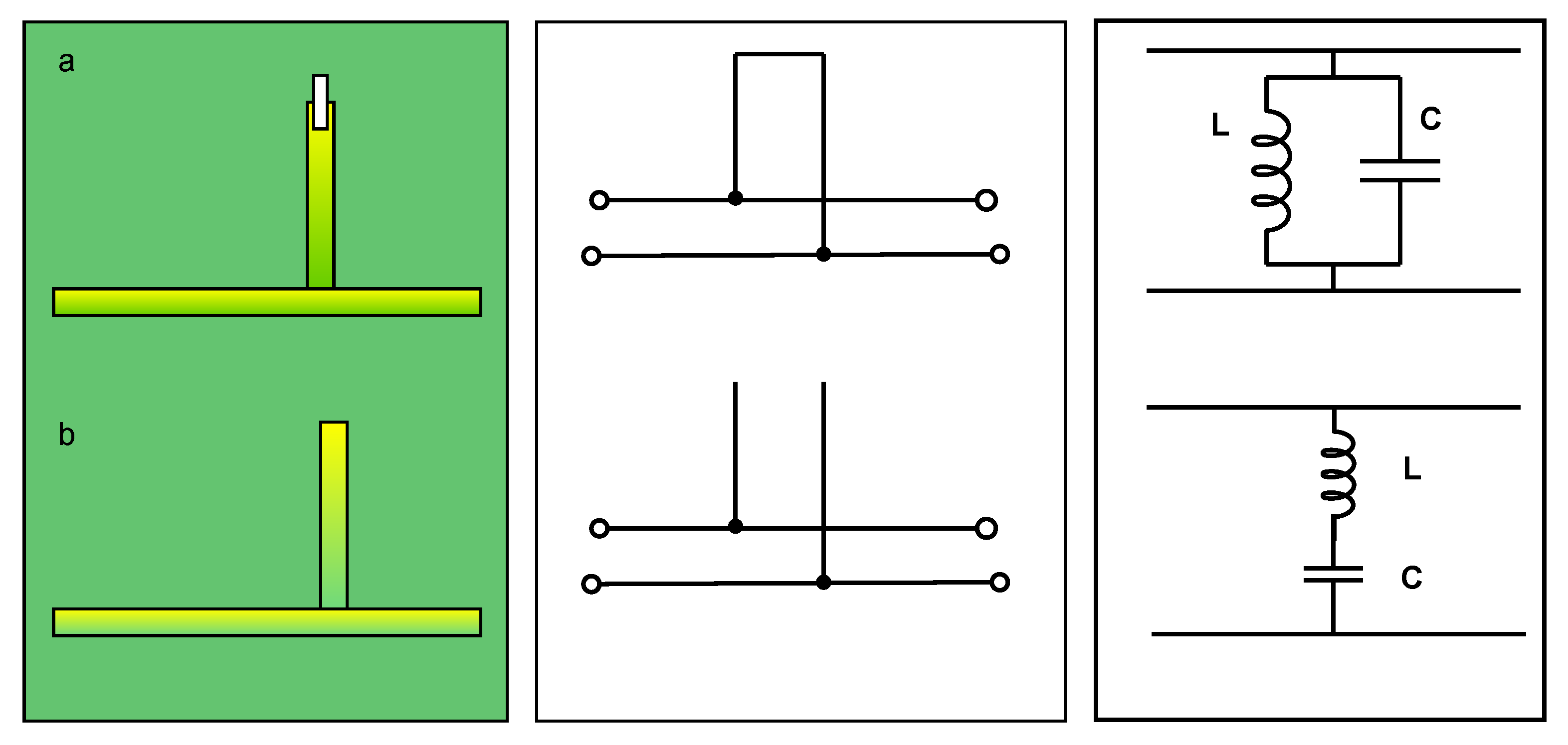
3.6. Impedance Matching Techniques and Trade-Offs in Low Noise Amplifier Design
4. The Proposed LNA Design and Simulation Results
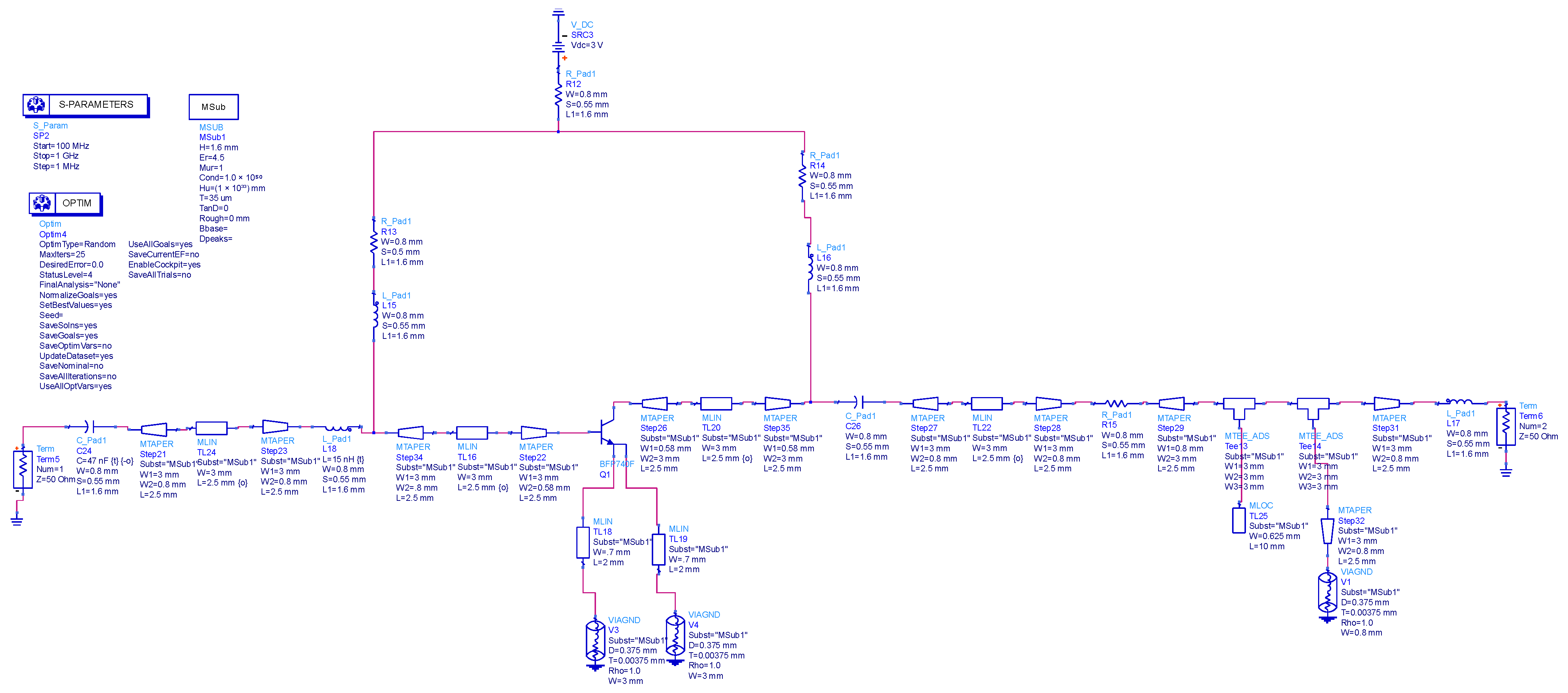
4.1. Common Emitter Single-Stage Transistor-Based LNA Topology
4.2. Simulation Results
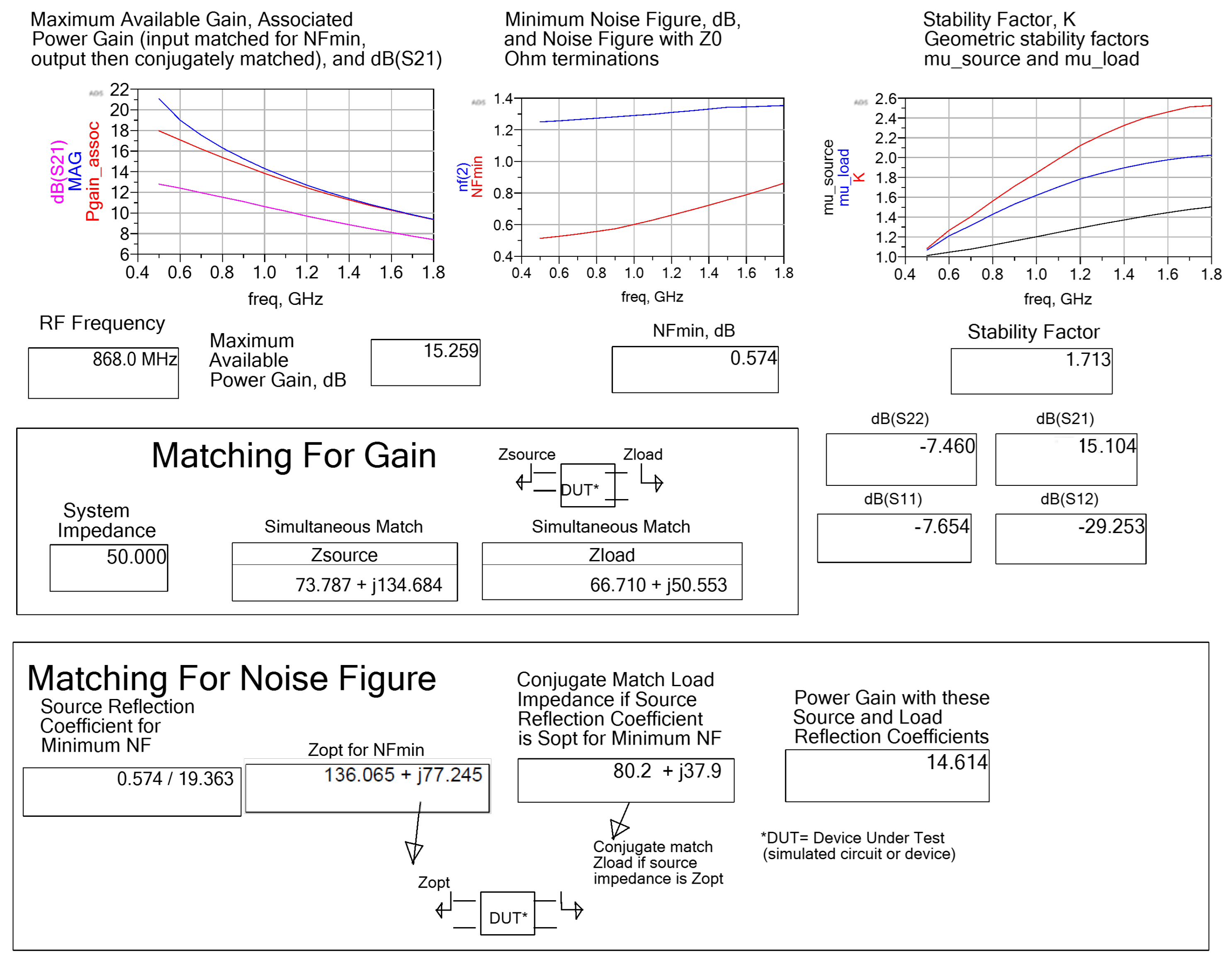
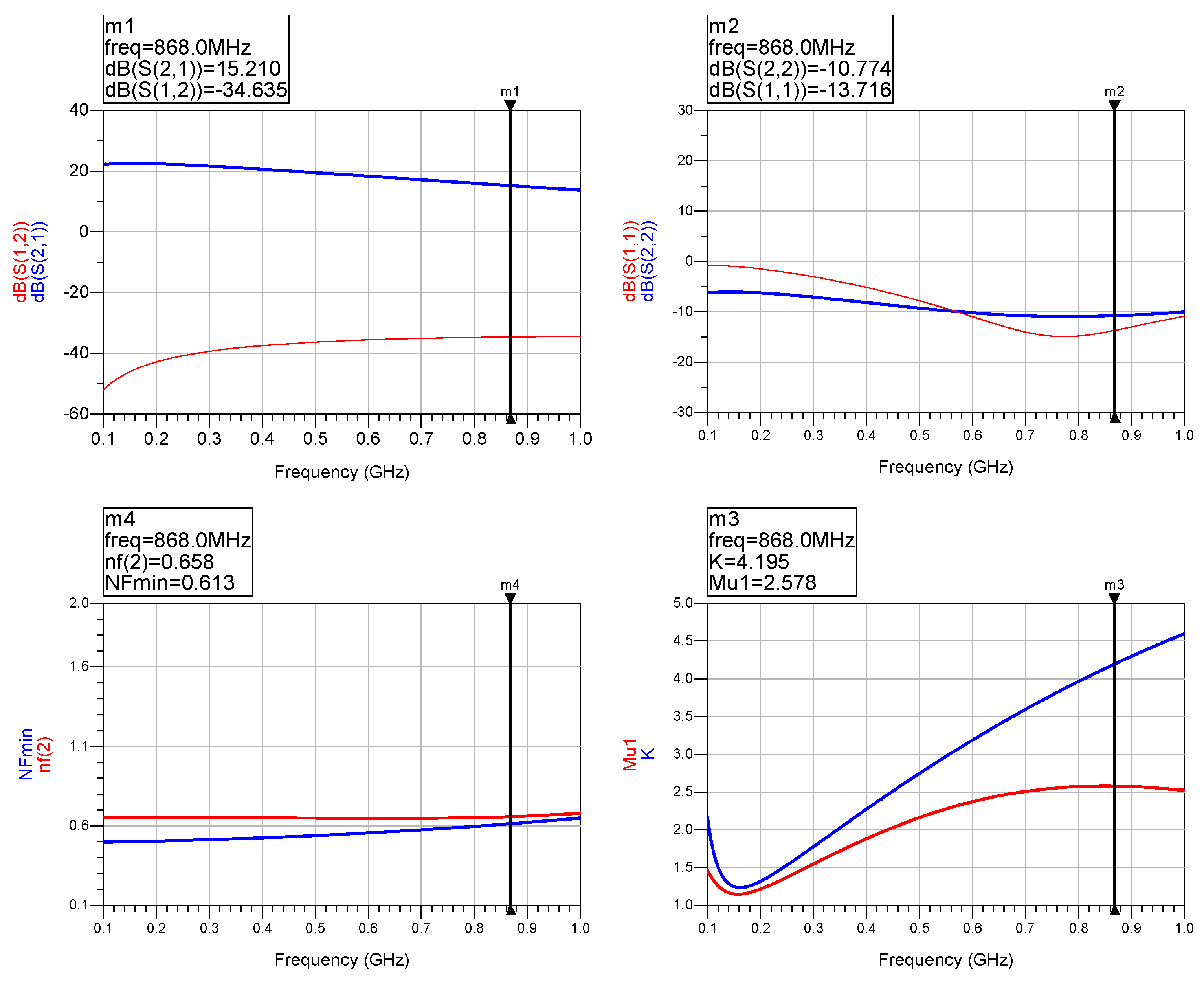
4.2.1. Circuit Biasing and Stability Analysis
4.2.2. Impedance Matching Design Using Complex Reflection Coefficients with Smith Chart and Stub Tuning
4.2.3. Full-Circuit Simulation and Layout Validation
5. Hardware Implementation and Real Measurement Results
5.1. Hardware Design and PCB Layout Design General Considerations
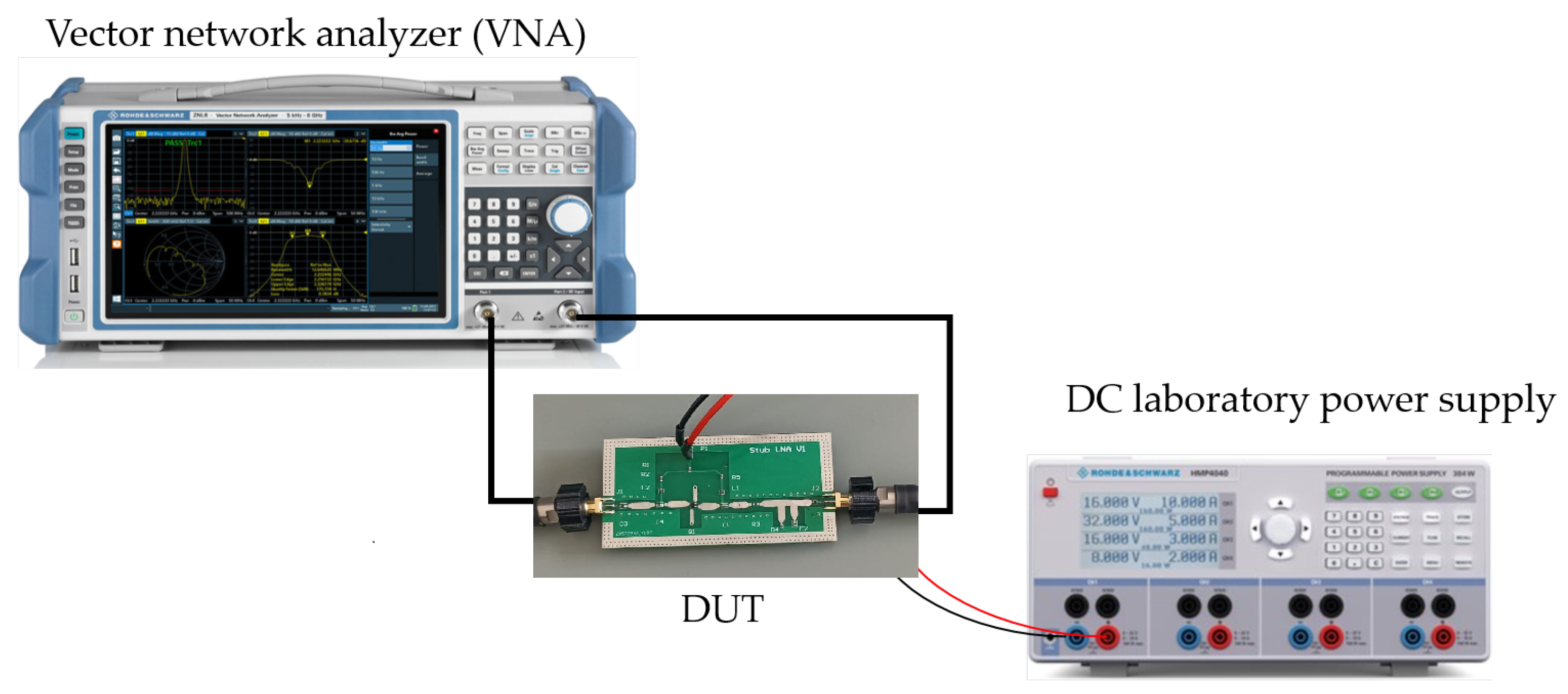
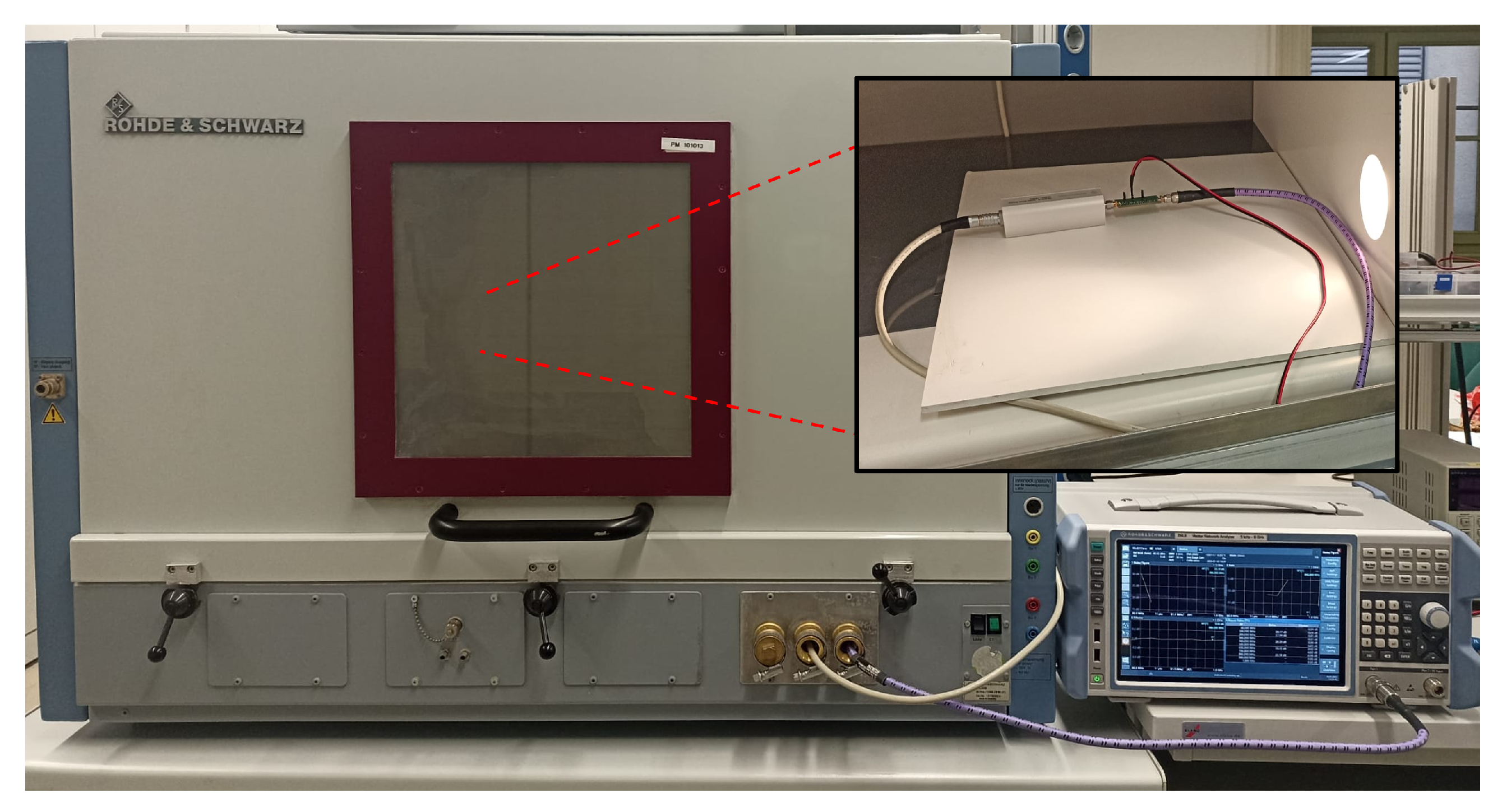
5.2. Measurement Setup and Performance Results
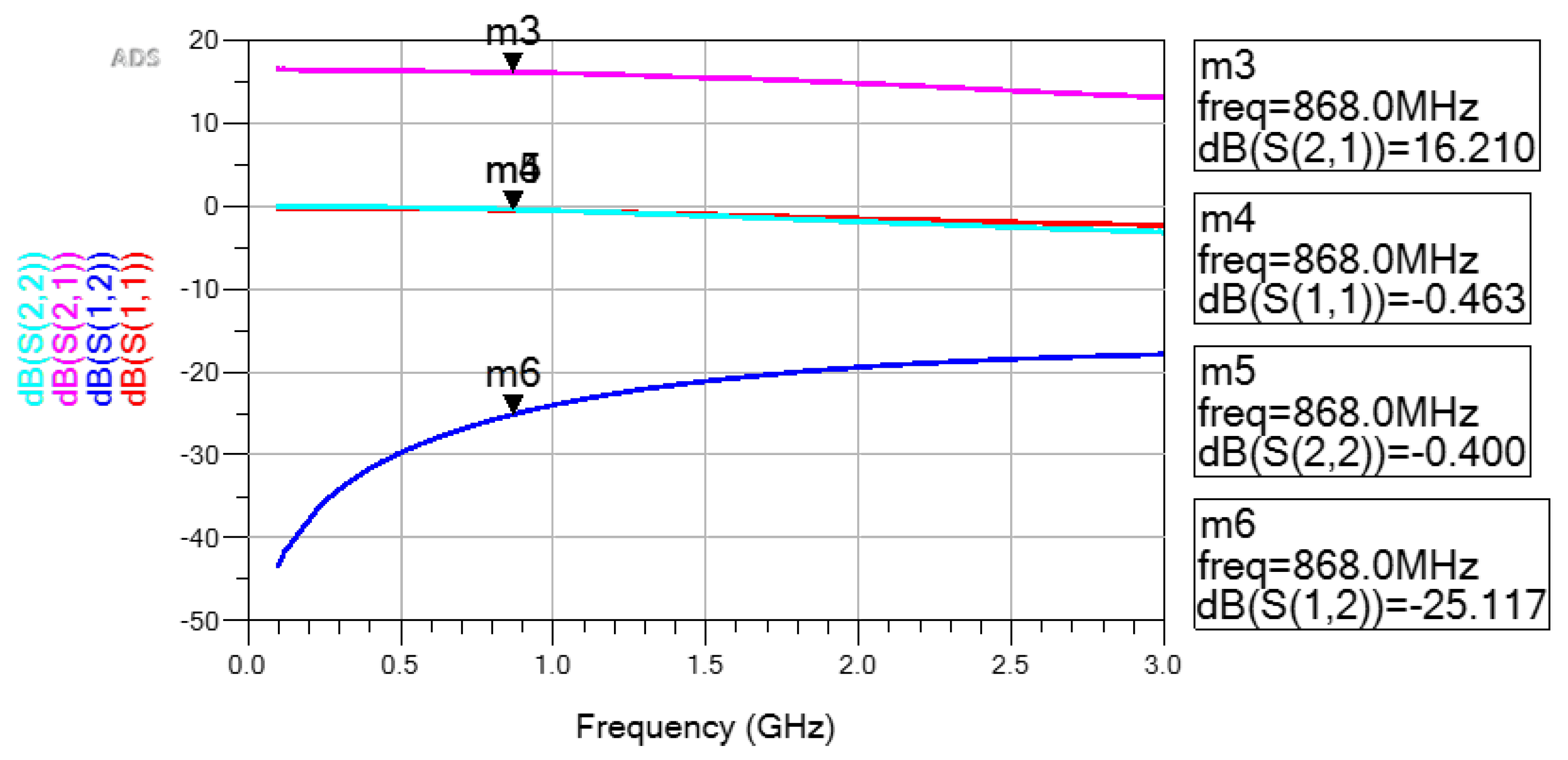
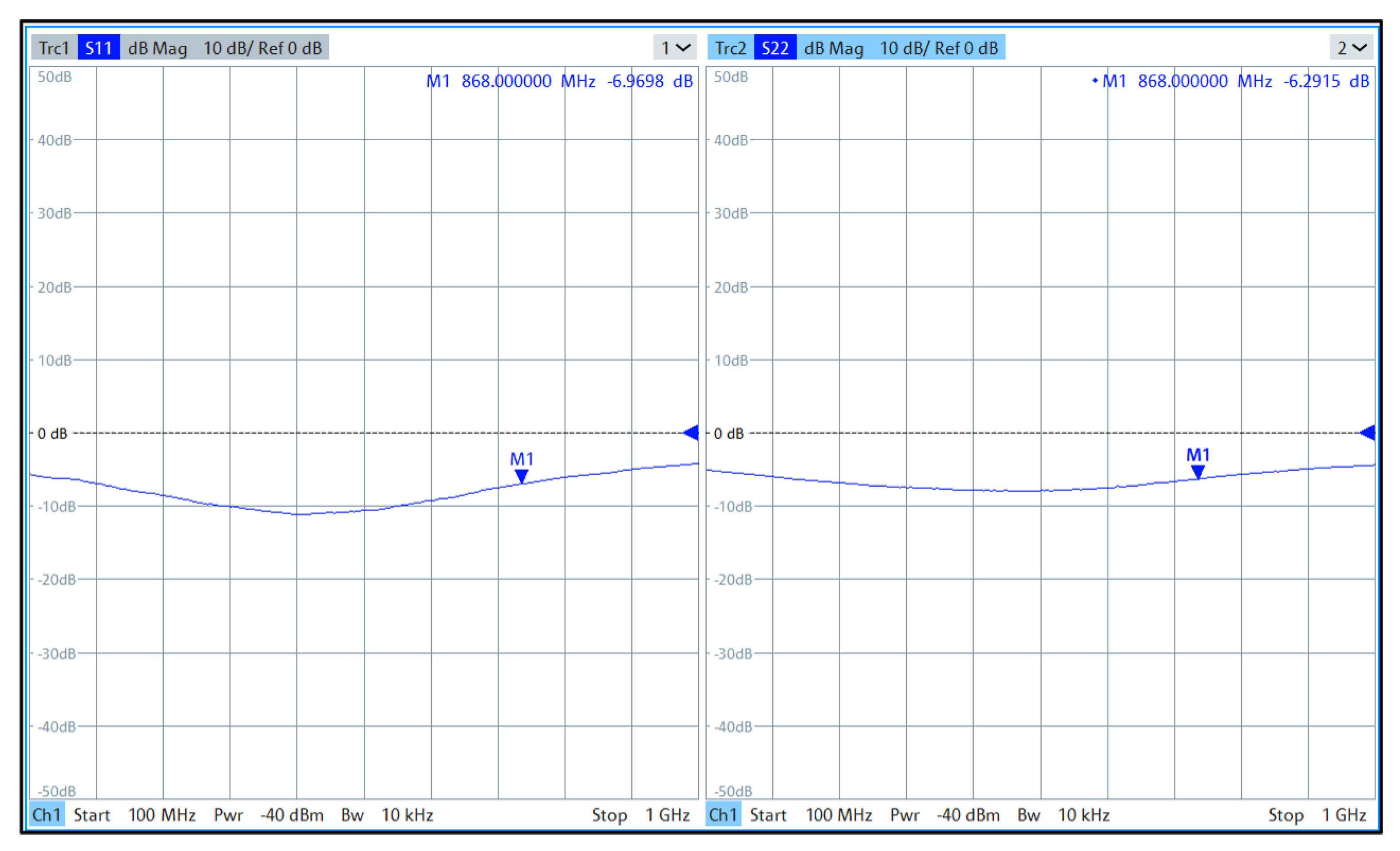
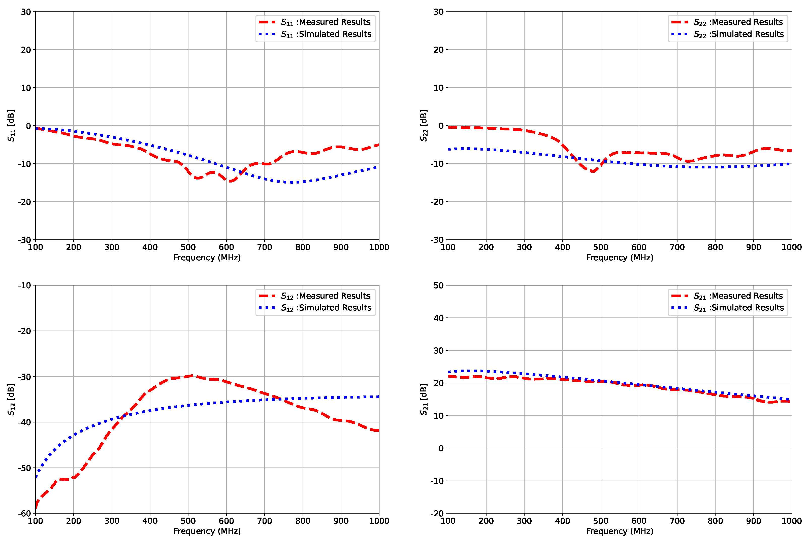
5.3. S-Parameters Simulated and Measured Results Comparison
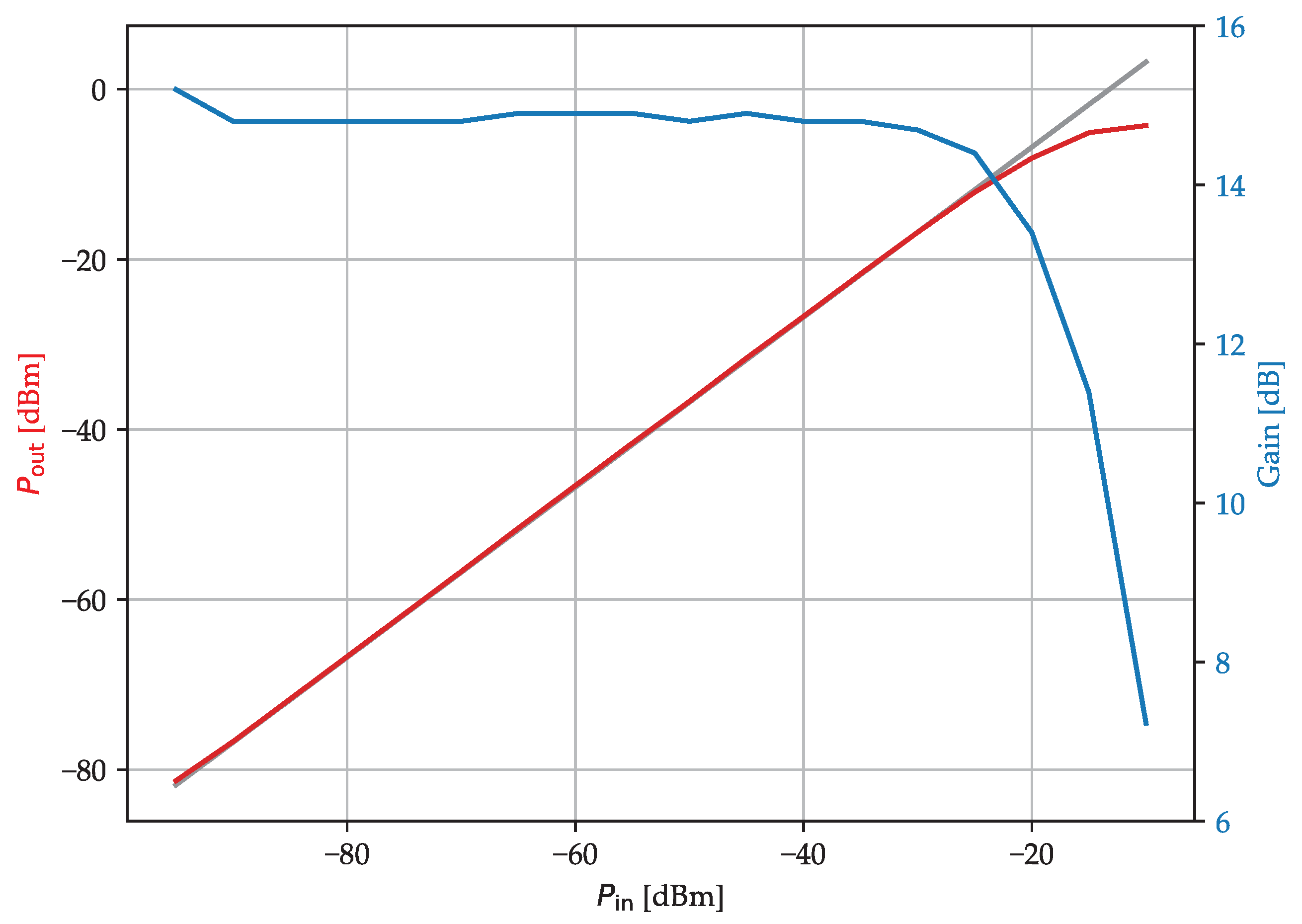
5.3.1. Performances of Gain with the Variation of Input Power
5.3.2. Noise Measurement Analysis
6. Conclusions
Author Contributions
Funding
Data Availability Statement
Acknowledgments
Conflicts of Interest
Abbreviations
| ADS | Advanced Design System |
| BJT | bipolar junction transistor |
| CE | common emitter |
| DUT | device under test |
| EMI | electromagnetic interference |
| ED | envelope detector |
| HBT | heterojunction bipolar transistor |
| IoT | internet of things |
| IMN | input-matching network |
| LNA | low-noise amplifier |
| MOSFET | Metal–Oxide–Semiconductor Field-Effect Transistor |
| NF | noise figure |
| OMN | output-matching network |
| PCB | printed circuit board |
| RF | radio frequency |
| SNR | signal-to-noise ratio |
| SoA | state of the art |
| TRF | tuned RF |
| VNA | Vector Network Analyzer |
| WSN | wireless sensor networks |
| WuRx | wake-up receiver |
| Wur | wake-up radio |
References
- Amutha, J.; Sharma, S.; Nagar, J. WSN strategies based on sensors, deployment, sensing models, coverage and energy efficiency: Review, approaches and open issues. Wirel. Pers. Commun. 2020, 111, 1089–1115. [Google Scholar] [CrossRef]
- Mercier, P.P.; Calhoun, B.H.; Wang, P.H.P.; Dissanayake, A.; Zhang, L.; Hall, D.A.; Bowers, S.M. Low-Power RF Wake-Up Receivers: Analysis, Tradeoffs, and Design. IEEE Open J. Solid-State Circuits Soc. 2022, 2, 144–164. [Google Scholar] [CrossRef]
- Zaraket, E.; Murad, N.M.; Yazdani, S.S.; Rajaoarisoa, L.; Ravelo, B. An overview on low energy wake-up radio technology: Active and passive circuits associated with MAC and routing protocols. J. Netw. Comput. Appl. 2021, 190, 103140. [Google Scholar] [CrossRef]
- Kozłowski, A.; Sosnowski, J. Energy efficiency trade-off between duty-cycling and wake-up radio techniques in IoT networks. Wirel. Pers. Commun. 2019, 107, 1951–1971. [Google Scholar] [CrossRef]
- D’Addato, M.; Antolini, A.; Renzini, F.; Elgani, A.M.; Perilli, L.; Scarselli, E.F.; Gnudi, A.; Magno, M.; Canegallo, R. Nanowatt Clock and Data Recovery for Ultra-Low Power Wake-Up Based Receivers. In Proceedings of the 2020 International Conference on Embedded Wireless Systems and Networks, Lyon, France, 17–19 February 2020; pp. 224–229. [Google Scholar]
- Chen, Y.; Ding, C.; Jia, Y.; Liu, Y. Antenna/propagation domain self-interference cancellation (SIC) for in-band full-duplex wireless communication systems. Sensors 2022, 22, 1699. [Google Scholar] [CrossRef] [PubMed]
- Dheerai, R.; Hiranmayee, K.B.; Praveena, K.S.; Dhanaraj, A.B.; Mallikarjuna, B.; Bhargavi, K. A Study on LNA, PLL and BPF of Front-End Integrated RF Receiver for Wireless Applications. In Proceedings of the 2021 6th International Conference on Communication and Electronics Systems (ICCES), Coimbatre, India, 8–10 July 2021; pp. 977–982. [Google Scholar] [CrossRef]
- Abbas, M.N.; Khaleel, F.A. Pre-low noise amplifier (LNA) filtering Linearisation method for low-power ultra-wideband complementary metal Oxide Semiconductor LNA. J. Eng. 2018, 2018, 342–347. [Google Scholar] [CrossRef]
- Chafai, O.; Nasri, M.W.; Barrak, R.; Ouerghemmi, S.; Ketata, I.; Derbel, F. Design of a Low-Noise Amplifier for Ultra Low Power Wake-Up Receiver in 868 MHz. In Proceedings of the 2023 20th International Multi-Conference on Systems, Signals & Devices (SSD), Mahdia, Tunisia, 20–23 February 2023; pp. 30–35. [Google Scholar] [CrossRef]
- Ouerghemmi, S.; Ketata, I.; Fakhfakh, A.; Derbel, F. Wide-Band Low-Noise Amplifier for reliable Wireless Sensor Networks. In Proceedings of the 2023 IEEE SENSORS, Vienna, Austria, 29 October–1 November 2023; pp. 1–4. [Google Scholar] [CrossRef]
- Schott, L.; Fromm, R.; Bouattour, G.; Kanoun, O.; Derbel, F. Analytical and Experimental Performance Analysis of Enhanced Wake-Up Receivers Based on Low-Power Base-Band Amplifiers. Sensors 2022, 22, 2169. [Google Scholar] [CrossRef] [PubMed]
- Ouerghemmi, S.; Fakhfakh, A.; Derbel, F. Design of a Low-Noise Amplifier for Ultra Low Power Wake-Up Receiver at 433 MHz. In Proceedings of the 2025 IEEE 22nd International Multi-Conference on Systems, Signals & Devices (SSD), Monastir, Tunisia, 17–20 February 2025; pp. 545–550. [Google Scholar] [CrossRef]
- Bansal, M.; Jyoti. A review of various applications of low noise amplifier. In Proceedings of the 2017 International Conference on Innovations in Control, Communication and Information Systems (ICICCI), Greater Noida, India, 12–13 August 2017; pp. 1–4. [Google Scholar] [CrossRef]
- Zhang, Y.; Demosthenous, A. Integrated circuits for medical ultrasound applications: Imaging and beyond. IEEE Trans. Biomed. Circuits Syst. 2021, 15, 838–858. [Google Scholar] [CrossRef] [PubMed]
- Qiu, W.; Chen, Y.; Wong, C.-M.; Liu, B.; Dai, J.; Zheng, H. A novel dual-frequency imaging method for intravascular ultrasound applications. Ultrasonics 2015, 57, 31–35. [Google Scholar] [CrossRef] [PubMed]
- Piyare, R.; Murphy, A.L.; Kiraly, C.; Tosato, P.; Brunelli, D. Ultra Low Power Wake-Up Radios: A Hardware and Networking Survey. IEEE Commun. Surv. Tutor. 2017, 19, 2117–2157. [Google Scholar] [CrossRef]
- Maruddani, B.; Ma’sum, M.; Sandi, E.; Taryana, Y.; Daniati, T.; Dara, W. Design of two stage low noise amplifier at 2.4–2.5 GHz frequency using microstrip line matching network method. J. Phys. Conf. Ser. 2019, 1402, 044031. [Google Scholar] [CrossRef]
- El Hardouzi, F.; Lahsaini, M.; Nasiri, B.; Bahich, M.; Achaoui, Y. Design of a broadband LNA with multifunction Circuitry based on composite right/left handed transmission lines for impedance matching and suppression of unwanted frequencies. Results Eng. 2024, 23, 102838. [Google Scholar] [CrossRef]
- Zhang, Y.; Lin, F.; Zeng, L. Optimal Design for Matching Network of L-band Low Noise Amplifier. In Proceedings of the 2016 International Forum on Mechanical, Control and Automation (IFMCA 2016), Shenzhen, China, 30–31 December 2016; Atlantis Press: Dordrecht, The Netherlands, 2017; pp. 1–9. [Google Scholar]
- Rahimian, A.; Pakdehi, D.M. Design and Realization of an S-Band Microwave Low-Noise Amplifier for Wireless RF Subsystems. arXiv 2014, arXiv:1409.2141. [Google Scholar]
- Chavan, M.B.; Patil, R.P. A Design and Analysis of Compact Microstrip Bandpass Filter with Integrated LNA for 0.8 to 2.7 GHZ. Int. J. Microw. Eng. (JMICRO) 2016, 1, 3. [Google Scholar] [CrossRef]
- Pozar, D.M. Microwave Engineering, 4th ed.; Wiley: Hoboken, NJ, USA, 2012. [Google Scholar]
- Lee, T.H. The Design of CMOS Radio-Frequency Integrated Circuits, 2nd ed.; Cambridge University Press: Cambridge, UK, 2004. [Google Scholar]
- Gonzalez, G. Microwave Transistor Amplifiers: Analysis and Design; Prentice Hall: Upper Saddle River, NJ, USA, 1997. [Google Scholar]
- Ball, E. Design and field trial measurement results for a portable and low cost VHF/UHF channel sounder platform for IoT propagation research. IET Microw. Antennas Propag. 2019, 13, 714–724. [Google Scholar] [CrossRef]
- Kusama, Y.; Isozaki, R. Compact and broadband microstrip band-stop filters with single rectangular stubs. Appl. Sci. 2019, 9, 248. [Google Scholar] [CrossRef]
- Mamedes, D.F.; Fernandes da Silva, J.P.; da Silva Souza, J.; da Silva Evangelista, T.; Rolim de Sousa, T.; Henrique da Fonseca Silva, P. Analysis of impedance matching techniques in tapered microstrip patch antenna. In Proceedings of the 2017 SBMO/IEEE MTT-S International Microwave and Optoelectronics Conference (IMOC), Aguas de Lindoia, Brazil, 27–30 August 2017; pp. 1–4. [Google Scholar] [CrossRef]


| Reference | Frequency Band (GHz) | Topology | Matching Network | Gain (dB) | Noise Figure (dB) | Power (mW) | Notable Features |
|---|---|---|---|---|---|---|---|
| [17] | 2.4–2.5 | Two-stage | Microstrip with single stub | ∼22 | 7.548 | 18 | Stub matching minimizes parasitic effects. |
| [18] | 1.9–2.8 | Single stage | CRLH-TLR * + SRR *** | 15.28 | 1.51 | 21 | Broadband design with composite microstrip structures. |
| [19] | L-band | Single stage | Lumped + Microstrip | NA ** | 0.35 | 25 | simulation layout using lumped and distributed elements. |
| [20] | 3.0 | Single stage | Microstrip | 13.32 | NA | 20 | Theoretical + CAD modeling for S-band operation. |
| [21] | 0.8–2.7 | Single stage | Microstrip | 15 | 3.85 | 12 | compact microstrip bandpass filter integrated with an LNA. |
| Element | Value/Description | Tolerance | Function/Selection Criteria |
|---|---|---|---|
| C1 | 47 nF | ±5% | AC coupling (input): Blocks DC and passes RF. Chosen for stability, low Equivalent Series Resistance (ESR), and high-frequency performance. |
| C2 | 1 nF | ±5% | AC coupling (output): Ensures DC isolation of output while passing RF; maintains low insertion loss. |
| L1 | 10 uH | ±5% | RF choke: Provides DC bias to collector while isolating RF. Selected to have Self Resonant Frequency(SRF) > 868 MHz. |
| L2 | 10 uH | ±5% | Output matching or resonance tuning: Optimized for S22 and gain flatness near 868 MHz. |
| L3 | 15–16 nH | ±5% | Input matching: Forms part of the matching network to transform source impedance to optimal noise/gain impedance. |
| L4 | 5.6 nH | ±5% | Input matching: Forms part of the matching network to transform source impedance to optimal noise/gain impedance. |
| R1 | 560 | ±5% | Collector bias: Supplies collector current via L1. Low noise and tight tolerance ensure consistent DC bias. |
| R2 | 47 kΩ | ±5% | Bias divider (upper leg): Together with R3, sets base voltage. Chosen for thermal stability. |
| R3 | 30 | ±5% | Bias divider (lower leg): Determines base bias voltage along with R2. Ensures proper VBE. |
| R4 | 10 | ±5% | Output stabilization: Provides broadband damping and helps prevent high-frequency oscillations. |
| Microstrip Matching Network | stubs ( at 868 MHz) | N/A | Series stubs (inductive) and shunt stubs (capacitive or resonant): Enable broadband impedance matching. Designed using for FR-4 (). |
| Emitter Ground Plane | Wide copper pour under emitter | N/A | Ensures low-impedance RF return path and minimizes parasitic inductance. Vital for gain stability and noise figure at microwave frequencies. |
| Parameters | Specifications | Simulation | Measured Results |
|---|---|---|---|
| Vcc (V) | 3.3 | 3.3 | 3.3 |
| Icc (mA) | <5 | 3.2 | 3.2 |
| Frequency Band (GHz) | 0.1–1 | 0.1–1 | 0.1–1 |
| Gain (dB) | >15 | 15.21 | 15.20 |
| Input Port Reflection (dB) | <−10 | −13.71 | −6.9 |
| Output Port Reflection (dB) | <−10 | −10.77 | −6.29 |
| Reverse Isolation (dB) | <−20 | <−32 | <−28 |
| Noise Figure (dB) | <2 | 0.65 | 1.77 |
Disclaimer/Publisher’s Note: The statements, opinions and data contained in all publications are solely those of the individual author(s) and contributor(s) and not of MDPI and/or the editor(s). MDPI and/or the editor(s) disclaim responsibility for any injury to people or property resulting from any ideas, methods, instructions or products referred to in the content. |
© 2025 by the authors. Licensee MDPI, Basel, Switzerland. This article is an open access article distributed under the terms and conditions of the Creative Commons Attribution (CC BY) license (https://creativecommons.org/licenses/by/4.0/).
Share and Cite
Ouerghemmi, S.; Fakhfakh, A.; Derbel, F. A Low-Power 868 MHz BJT-Based LNA with Microstrip Matching for Wake-Up Receivers in IoT Applications. Electronics 2025, 14, 2429. https://doi.org/10.3390/electronics14122429
Ouerghemmi S, Fakhfakh A, Derbel F. A Low-Power 868 MHz BJT-Based LNA with Microstrip Matching for Wake-Up Receivers in IoT Applications. Electronics. 2025; 14(12):2429. https://doi.org/10.3390/electronics14122429
Chicago/Turabian StyleOuerghemmi, Sarah, Ahmed Fakhfakh, and Faouzi Derbel. 2025. "A Low-Power 868 MHz BJT-Based LNA with Microstrip Matching for Wake-Up Receivers in IoT Applications" Electronics 14, no. 12: 2429. https://doi.org/10.3390/electronics14122429
APA StyleOuerghemmi, S., Fakhfakh, A., & Derbel, F. (2025). A Low-Power 868 MHz BJT-Based LNA with Microstrip Matching for Wake-Up Receivers in IoT Applications. Electronics, 14(12), 2429. https://doi.org/10.3390/electronics14122429