
State-of-the-Art VCO with Eight-Shaped Resonator-Type Transmission Line

Abstract
1. Introduction
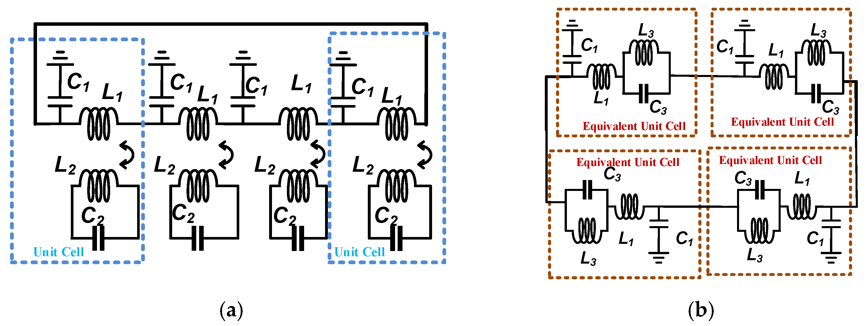
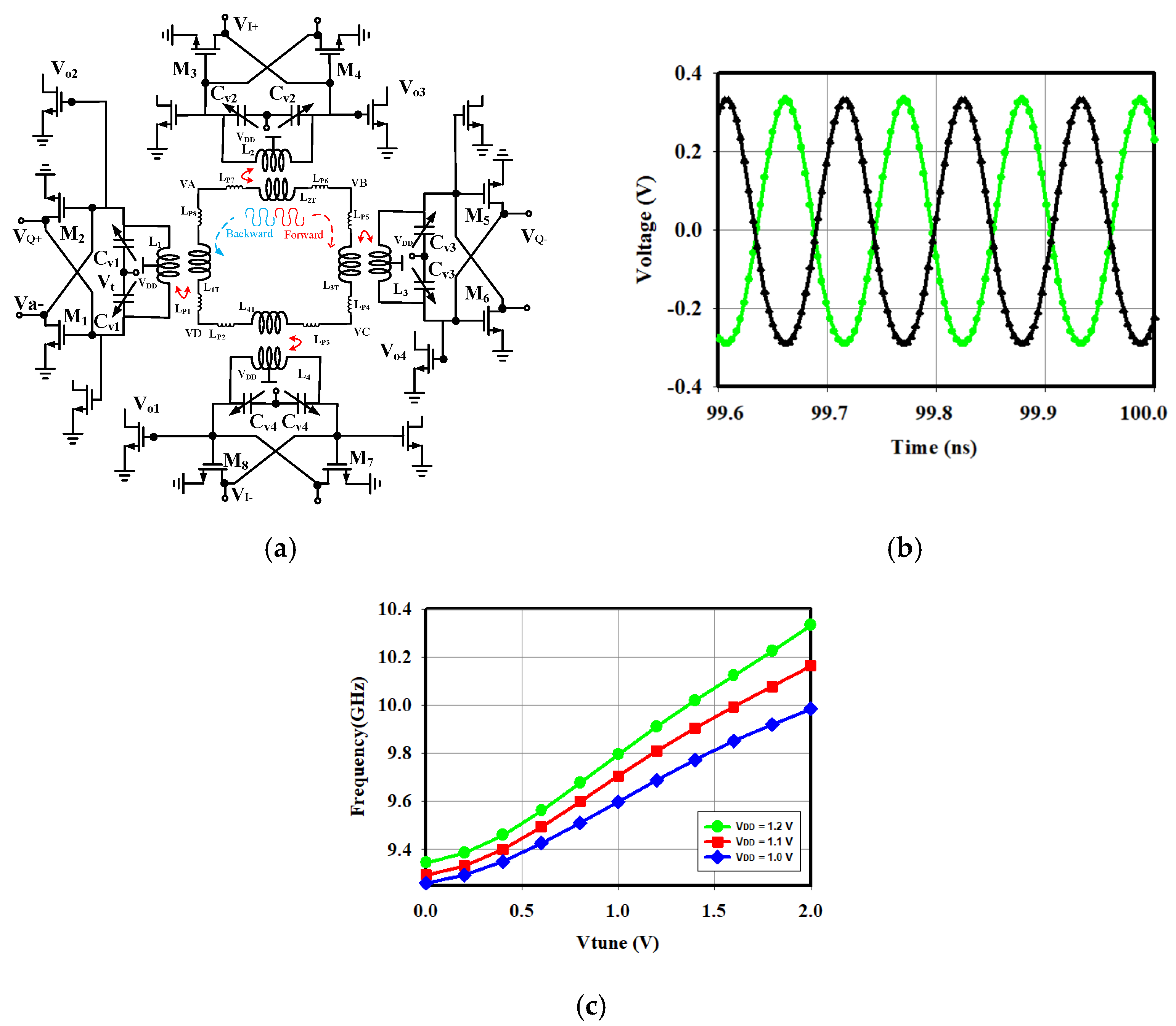
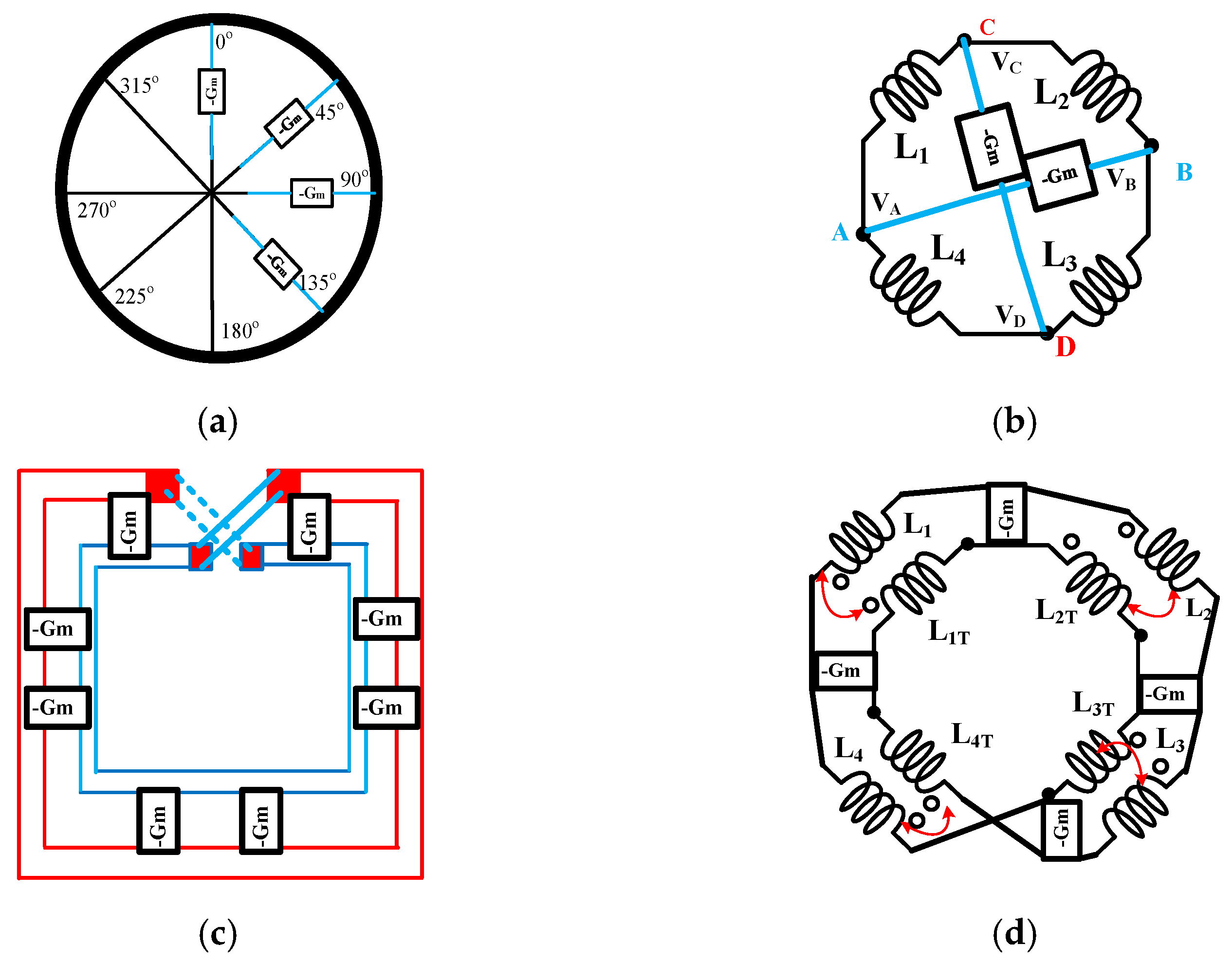
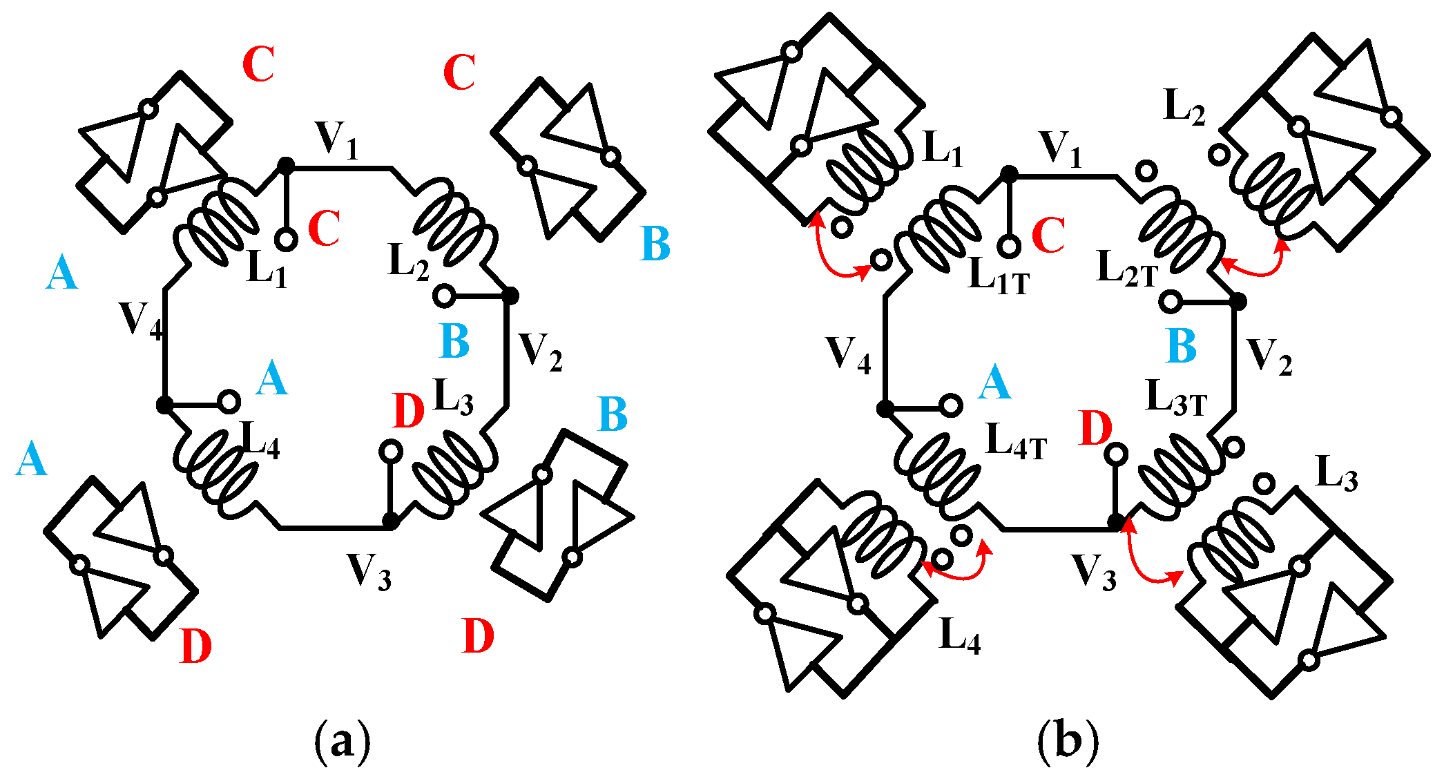
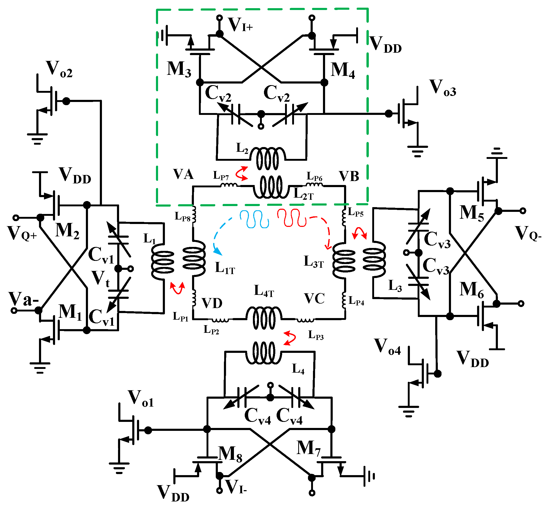
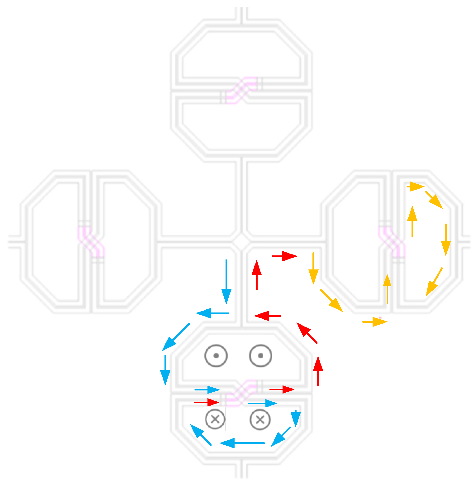
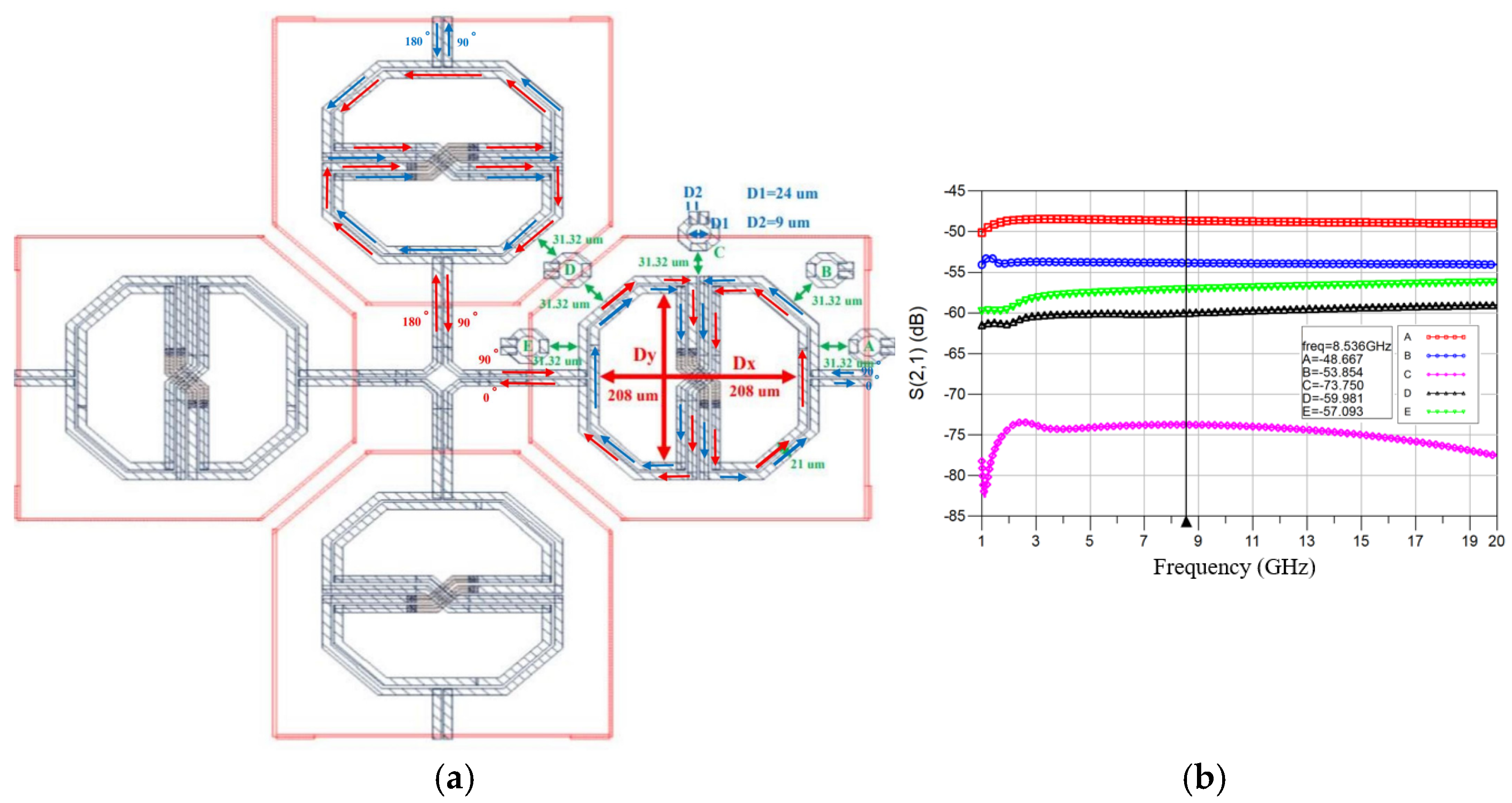
2. Circuit Design
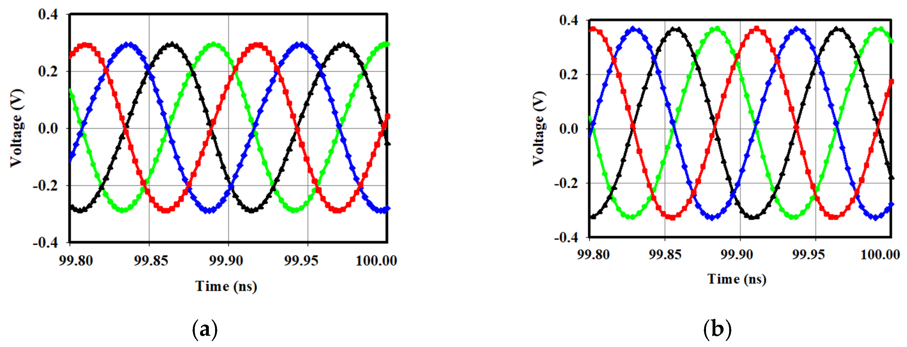
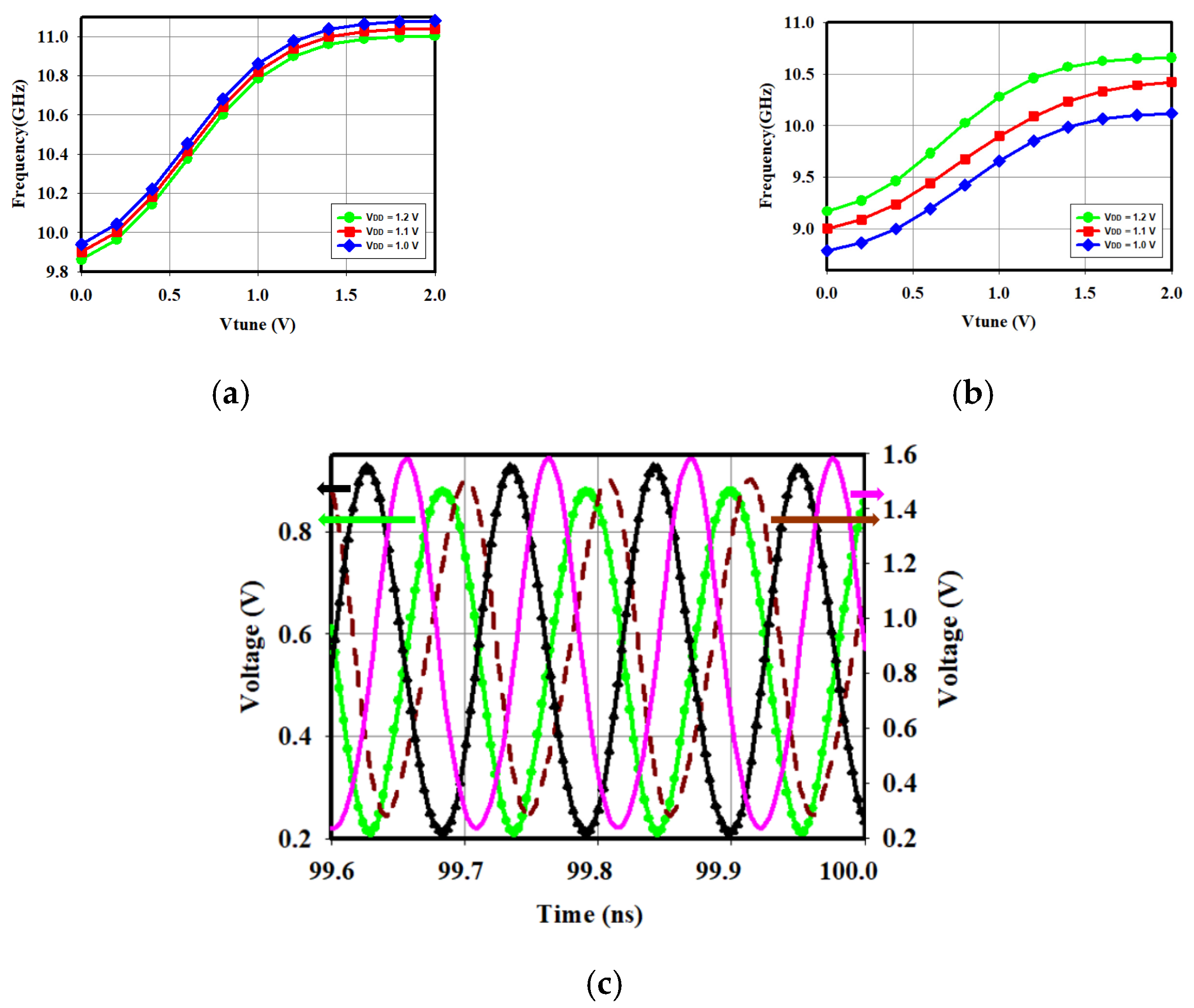
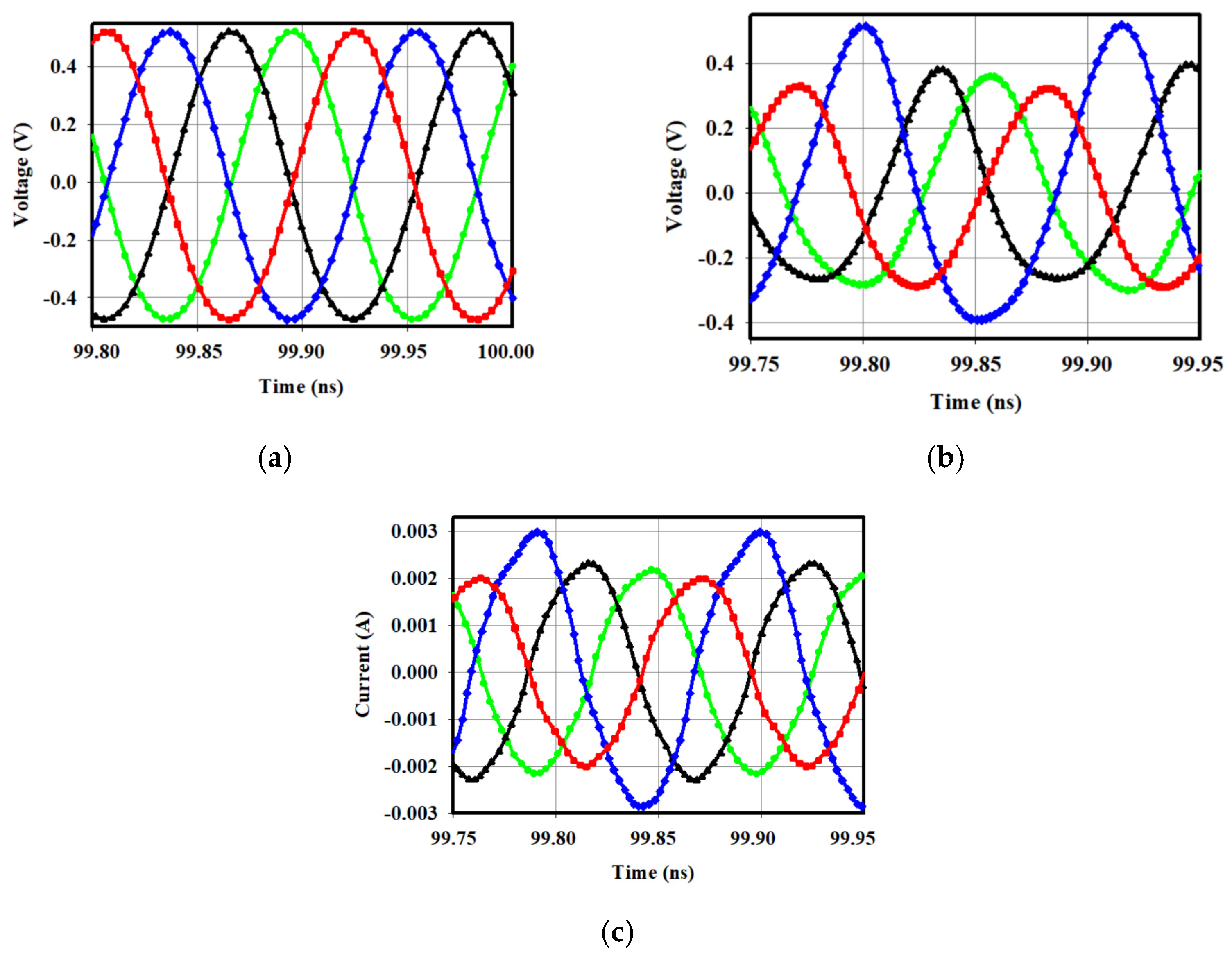
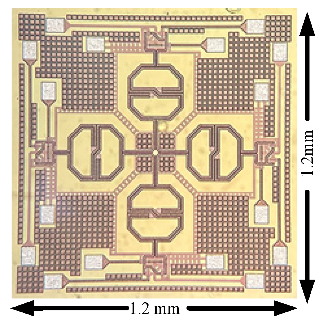
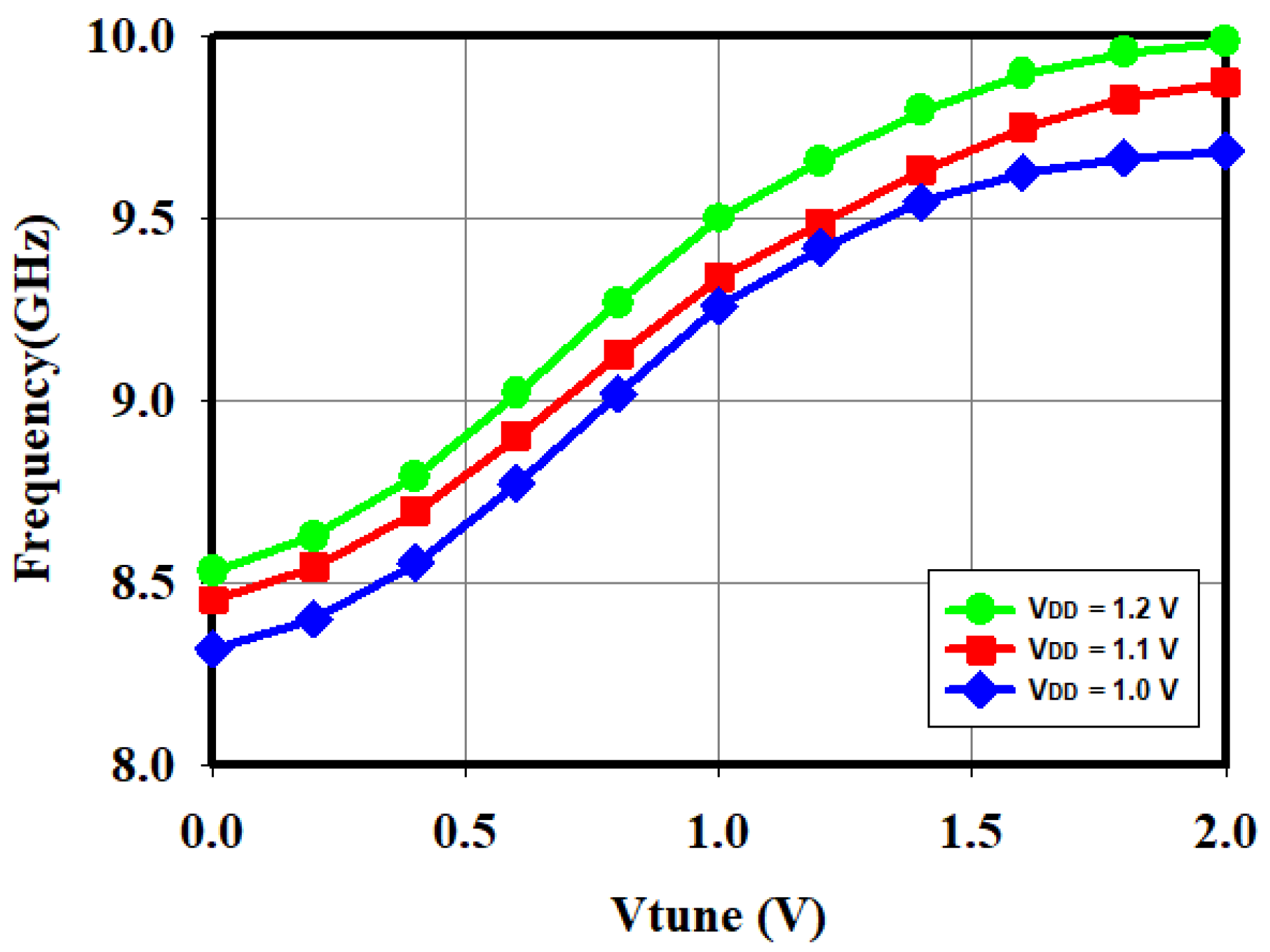
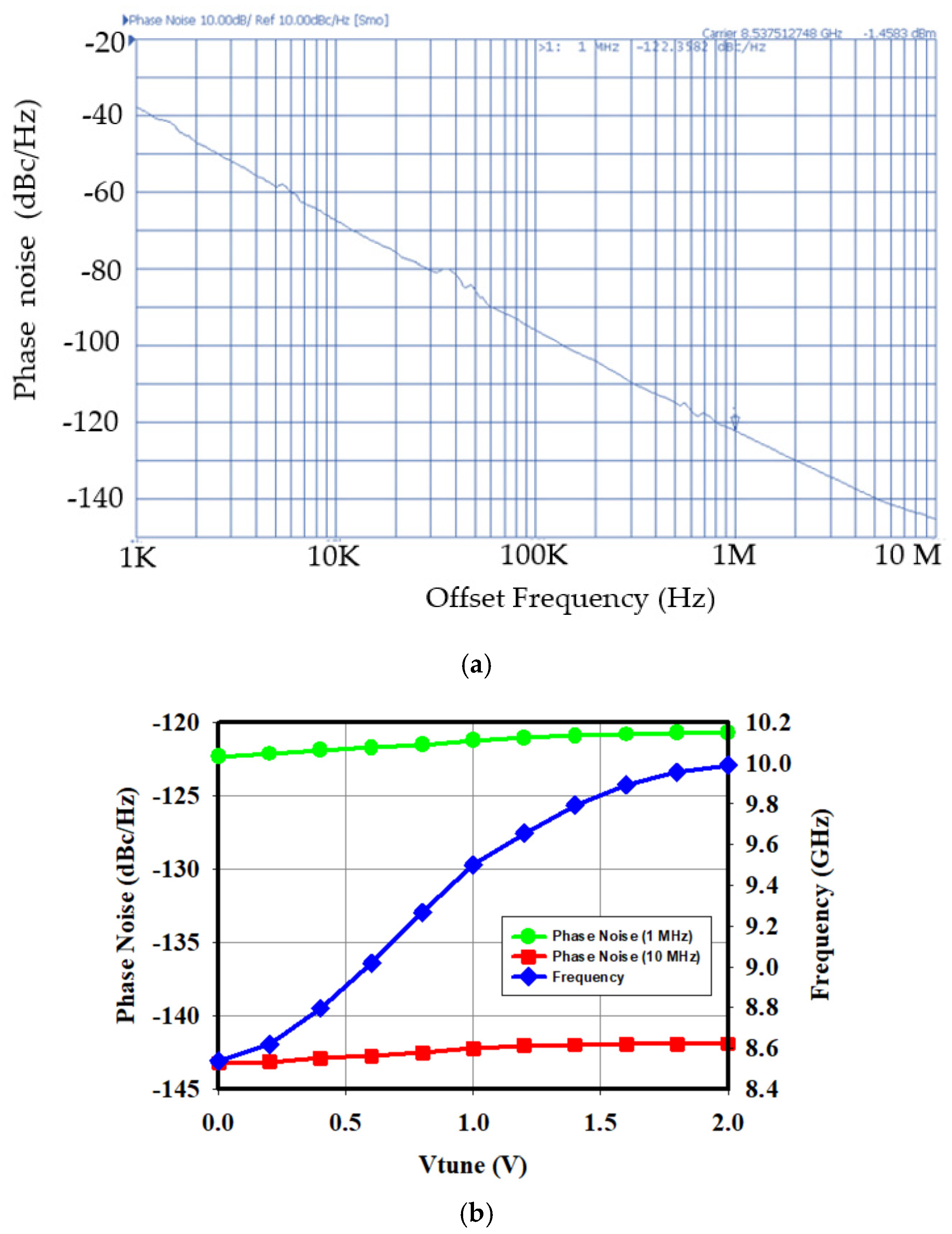
3. Experimental Results
4. Conclusions
Author Contributions
Funding
Data Availability Statement
Acknowledgments
Conflicts of Interest
Appendix A
References
- Zou, W.; Zou, X.; Ren, D.; Zhang, K.; Liu, D.; Ren, Z. 2.49–4.91 GHz wideband VCO with an optimized 8-shaped inductor. Electron. Lett. 2019, 55, 55–57. [Google Scholar] [CrossRef]
- Mahmoud, A.; Fanori, L.; Mattsson, T.; Caputa, P.; Andreani, P. A 2.8-to-5.8 GHz harmonic VCO based on an 8-shaped inductor in a 28 nm UTBB FD-SOI CMOS process. Analog. Integr. Circuits Signal Process. 2016, 88, 391–399. [Google Scholar] [CrossRef]
- Neihart, N.M.; Allstot, D.J.; Miller, M.; Rakers, P. Twisted transformers for low coupling RF and mixed-signal applications. In Proceedings of the 2009 IEEE International Symposium on Circuits and Systems, Taipei, Taiwan, 24–27 May 2009; pp. 429–432. [Google Scholar] [CrossRef]
- Wang, P.-Y.; Wu, T.-L.; Chen, M.-Y.; Shen, Y.-C.; Chang, Y.-C.; Chang, D.-C.; Hsu, S.S.H. A low-phase-noise class-C VCO using a novel 8-shaped transformer. In Proceedings of the 2015 IEEE International Symposium on Circuits and Systems (ISCAS), Lisbon, Portugal, 24–27 May 2015; pp. 886–889. [Google Scholar]
- Itoh, N.; Hideaki; Masuoka; Fukase, S.-I.; Hirashiki, K.-I.; Nagata, M. Twisted inductor VCO for suppressing on-chip interferences. In Proceedings of the 2007 Asia-Pacific Microwave Conference, Bangkok, Thailand, 11–14 December 2007; pp. 1–4. [Google Scholar] [CrossRef]
- Gathman, D.; Buckwalter, J.F. A 92-GHz deterministic quadrature oscillator and N-push modulator in 120-nm SiGe BiCMOS. In Proceedings of the 2013 IEEE/MTT-S International Microwave Symposium, Seattle, WA, USA, 2–7 June 2013; pp. 1–4. [Google Scholar]
- Zhang, C.; Wang, Z.; Zhao, Y.; Park, S.M. A 15 GHz, −182 dBc/Hz/mW FOM, Rotary Traveling Wave VCO in 90 nm CMOS. IEEE Microw. Wirel. Compon. Lett. 2012, 22, 206–208. [Google Scholar] [CrossRef]
- Wood, J.; Edwards, T.; Lipa, S. Rotary traveling-wave oscillator arrays: A new clock technology. IEEE J. Solid-State Circuits 2001, 36, 1654–1665. [Google Scholar] [CrossRef]
- Shehata, M.A.; Roy, V.; Breslin, J.; Shanan, H.; Keaveney, M.; Staszewski, R.B. A 32–42-GHz RTWO-based frequency quadrupler achieving >37 dBc harmonic rejection in 22-nm FD-SOI. IEEE Solid-State Circuits Lett. 2021, 4, 72–75. [Google Scholar] [CrossRef]
- Rabbi, F.; Xie, Z.; Dogan, N.S. A 42/84-GHz multi-ring rotary traveling-wave oscillator design in 0.13-µm BiCMOS. Analog. Integr. Circuits Signal Process. 2019, 100, 577–592. [Google Scholar] [CrossRef]
- Bai, Z.; Zhou, X.; Mason, R.D.; Allan, G. A 2-GHz pulse injection-locked rotary traveling-wave oscillator. IEEE Trans. Microw. Theory Tech. 2016, 64, 1854–1866. [Google Scholar] [CrossRef]
- Bai, Z.; Zhou, X.; Mason, R.D.; Allan, G. Low-phase noise clock distribution network using rotary traveling-wave oscillators and built-in self-test phase tuning technique. IEEE Trans. Circuits Syst. II Express Briefs 2015, 62, 41–45. [Google Scholar] [CrossRef]
- Lai, W.-C.; Jang, S.-L.; Syu, J.-W. Quadrature VCO via transformer-coupled transmission line. In Proceedings of the 2019 12th International Workshop on the Electromagnetic Compatibility of Integrated Circuits (EMC Compo), Hangzhou, China, 21–23 October 2019; pp. 2–5. [Google Scholar] [CrossRef]
- Lai, W.-C.; Jang, S.-L.; Wang, J.-J. Dual band quadrature VCO using switched-transformer coupling for wireless robot applications. In Proceedings of the 2019 4th Asia-Pacific Conference on Intelligent Robot Systems (ACIRS), Nagoya, Japan, 13–15 July 2019; pp. 109–112. [Google Scholar] [CrossRef]
- Jang, S.L.; Lin, S.S.; Chang, C.W.; Hsu, S.H. A complementary cross-coupled quadrature VCO using ring inductor coupling method. Microw. Opt. Technol. Lett. 2012, 54, 839–842. [Google Scholar] [CrossRef]
- Lee, J.; Razavi, B. A 40 Gb/s clock and data recovery circuit in 0.18-µm CMOS technology. In Proceedings of the Digest of Technical Papers IEEE International Solid-State Circuits Conference (ISSCC’03), San Francisco, CA, USA, 3–7 February 2003; pp. 242–243. [Google Scholar]
- Takinami, K.; Walsworth, R.; Osman, S.; Beccue, S. Phase-noise analysis in rotary traveling-wave oscillators using simple physical model. IEEE Trans. Microw. Theory Tech. 2010, 58, 1465–1474. [Google Scholar] [CrossRef]
- Peng, Y.Y.; Yu, X.P.; Gu, J.M.; Lim, W.M.; Sui, W.Q. An area-efficient CRLH (composite right/left-handed)-TL approach to the design of rotary traveling-wave oscillator. IEEE Microw. Wirel. Components Lett. 2013, 23, 560–562. [Google Scholar] [CrossRef]
- Ben Abdeljelil, F.; Tatinian, W.; Carpineto, L.; Jacquemod, G. Design of a CMOS 12 GHz rotary travelling wave oscillator with switched capacitor tuning. In Proceedings of the 2009 IEEE Radio Frequency Integrated Circuits Symposium (RFIC), Boston, MA, USA, 7–9 June 2009; pp. 579–582. [Google Scholar] [CrossRef]
- Ansari, K.T.; Ross, T.N.; Plett, C. Ku-band high output power multiphase rotary traveling-wave VCO in SiGe BiCMOS. In Proceedings of the Microwave Integrated Circuits Conference (EuMIC), 2013 European, Nuremberg, Germany, 6–8 October 2013; pp. 97–100. [Google Scholar]
- Hu, X.; Dai, Y.; Zhang, H.; Zhou, J.; Chen, K. Rotary traveling-wave oscillator design using 0.18 μm CMOS. J. Semicond. 2010, 31, 065009. [Google Scholar]
- Ansari, K.T.; Ross, T.; Gamand, P.; Plett, C. Frequency domain phase shift measurement technique applied to a multiphase rotary travelling-wave VCO. IEEE Microw. Wirel. Components Lett. 2015, 25, 820–822. [Google Scholar] [CrossRef]
- Shehata, M.A.; Keaveney, M.; Staszewski, R.B. A Distributed stubs technique to mitigate flicker noise upconversion in a mm-wave rotary traveling-wave oscillator. IEEE J. Solid-state Circuits 2021, 56, 1745–1760. [Google Scholar] [CrossRef]
- Shehata, M.A.; Keaveney, M.; Staszewski, R.B. A 184.6-dBc/Hz FoM 100-kHz flicker phase noise corner 30-GHz rotary traveling-wave oscillator using distributed stubs in 22-nm FD-SOI. IEEE Solid-State Circuits Lett. 2019, 2, 103–106. [Google Scholar] [CrossRef]
- Li, H.; Shu, Y.; Pi, C.; Luo, X. A 19.1–25.5-GHz compact dual-mode rotary traveling-wave oscillator with 195.4-dBc/Hz FoM. IEEE Microw. Wirel. Components Lett. 2022, 32, 1347–1350. [Google Scholar] [CrossRef]
- Chien, J.-C.; Lu, L.-H. A 32-GHz rotary traveling-wave voltage controlled oscillator in 0.18-μm CMOS. IEEE Microw. Wirel. Compon. Lett. 2007, 17, 724–726. [Google Scholar] [CrossRef]
- Nouri, N.; Buckwalter, J.F. A 45-GHz rotary-wave voltage-controlled oscillator. IEEE Trans. Microw. Theory Tech. 2011, 59, 383–392. [Google Scholar] [CrossRef]
- Sun, F.; Zhou, Y.; Bai, Z.; Chen, Y. A 190.3-dBc/Hz FoM 16-GHz rotary traveling-wave oscillator with reliable direction control. IET Electron. Lett. 2021, 57, 209–211. [Google Scholar] [CrossRef]
- Vigilante, M.; Reynaert, P. A Coupled-RTWO-based subharmonic receiver front end for 5G $E$-band backhaul links in 28-nm bulk CMOS. IEEE J. Solid-State Circuits 2018, 53, 2927–2938. [Google Scholar] [CrossRef]
- Galeone, S.; Kennedy, M.P.; Ahmed, K.; Shanan, H.; Keaveney, M. An eight-phase 40GHz RTWO in 28 nm CMOS with phase noise reduction via head and tail filtering. In Proceedings of the 2019 26th IEEE International Conference on Electronics, Circuits and Systems (ICECS), Genoa, Italy, 27–29 November 2019; pp. 306–309. [Google Scholar] [CrossRef]
- Jang, S.-L.; Chen, S.-H.; Sung, J.-Y.; Lai, W.-C.; Hsu, M.-H.; Juang, M.-H. VCO with 8-shaped transformer coupled transmission line. In Proceedings of the 2024 IEEE Asia Pacific Conference on Circuits and Systems (APCCAS), Taipei, Taiwan, 7–9 November 2024; pp. 277–280. [Google Scholar]
- Jahan, N.; Barakat, A.; Pokharel, R.K. Design of Low Phase Noise VCO Considering C/L Ratio of LC Resonator in 0.18-μm CMOS Technology. IEEE Trans. Circuits Syst. II Express Briefs 2021, 68, 3513–3517. [Google Scholar] [CrossRef]


| Ref. | Tech (μm) | fosc (GHz) | Vdd(V) Pdis, mW | Area (mm2) | PN @ 1 MHz dBc/Hz | FOM dBc/Hz |
|---|---|---|---|---|---|---|
| [6] | 0.09 | 15.0 | 1.2/12 | 0.45 × 0.45 | −109.6 | −182.0 |
| [12] | 0.18 | 3.26 | 1.0/5.33 | 1.07 × 1.07 | −122.14 | −185.11 |
| [13] | 0.18 | 2.79 | 1.1/4.78 | 1.2 × 1.2 | −121.4 | −181.8 |
| [14] | 0.18 | 23.6 | 1.8/70.2 | 0.8 | −105.0 | −164 |
| [19] | 0.13 | 12.2 | 1.2/30 | 0.3 × 0.35 | −105.2 | −171.95 |
| [20] | 0.25 | 18 | 4/54 | − | −98.0 | −98.0 |
| [21] | 0.18 | 5.28 | 1.8/129 | 1.5 × 1.5 | −102.0 | −155.35 |
| [22] | 0.25Bi | 18.5 | 1/38.4 | − | −103.5 | − |
| [23] | 0.022 | 26.2 | 0.8/21 | 0.24 | −108.5 | −183.6 |
| [24] | 0.022 | 26.2 | 0.8/20 | 0.24 core | −109.2 | −184.2 |
| [25] | 0.04 | 19.1 | 1.1/16.6 | 0.08 core | −106.4 | |
| [26] | 0.18 | 32 | 1.2/54 | 1.3 × 1.3 | −108.0 | −177.7 |
| [27] | 0.12 | 45 | 1.2/19.2 | 0.25 | −93 | −173.0 |
| [28] | 0.13 | 16.2 | 1.2/5.8 | simulated | −113.7 | −190.3 |
| [29] | 0.028 | 19.8 | 1.3/75 | − | −101.2 | −168.4 |
| [30] | 0.13 | 37.7 | −/16.2 | − | −121@10 | −180.6 |
| [31] | 0.18 | 3.4 | 1.7/19.2 | 1.2 × 1.2 | −125.7 | −185.4 |
| [32] | 0.18 | 17.5 | −/2.3 | 0.56 × 0.183 (core) | −110.77 | −191.95 |
| This | 0.18 | 8.53 | 1.7/5.84 | 1.2 × 1.2 | −122.4 | −193.4 |
Disclaimer/Publisher’s Note: The statements, opinions and data contained in all publications are solely those of the individual author(s) and contributor(s) and not of MDPI and/or the editor(s). MDPI and/or the editor(s) disclaim responsibility for any injury to people or property resulting from any ideas, methods, instructions or products referred to in the content. |
© 2025 by the authors. Licensee MDPI, Basel, Switzerland. This article is an open access article distributed under the terms and conditions of the Creative Commons Attribution (CC BY) license (https://creativecommons.org/licenses/by/4.0/).
Share and Cite
Jang, S.-L.; Lin, Z.-J.; Juang, M.-H. State-of-the-Art VCO with Eight-Shaped Resonator-Type Transmission Line. Electronics 2025, 14, 2322. https://doi.org/10.3390/electronics14122322
Jang S-L, Lin Z-J, Juang M-H. State-of-the-Art VCO with Eight-Shaped Resonator-Type Transmission Line. Electronics. 2025; 14(12):2322. https://doi.org/10.3390/electronics14122322
Chicago/Turabian StyleJang, Sheng-Lyang, Zi-Jun Lin, and Miin-Horng Juang. 2025. "State-of-the-Art VCO with Eight-Shaped Resonator-Type Transmission Line" Electronics 14, no. 12: 2322. https://doi.org/10.3390/electronics14122322
APA StyleJang, S.-L., Lin, Z.-J., & Juang, M.-H. (2025). State-of-the-Art VCO with Eight-Shaped Resonator-Type Transmission Line. Electronics, 14(12), 2322. https://doi.org/10.3390/electronics14122322