
Left-Hand Resonator VCO Using an Orthogonal Transformer


Abstract
1. Introduction
2. Left-Hand Resonator VCO Using Two O-Shaped Inductors
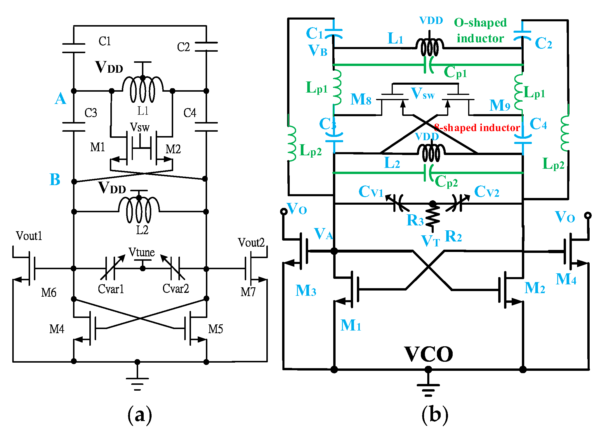
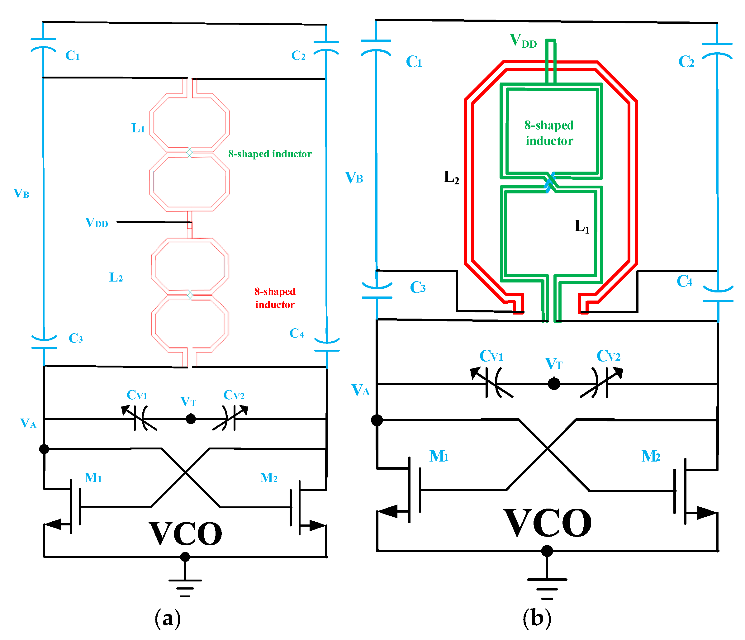
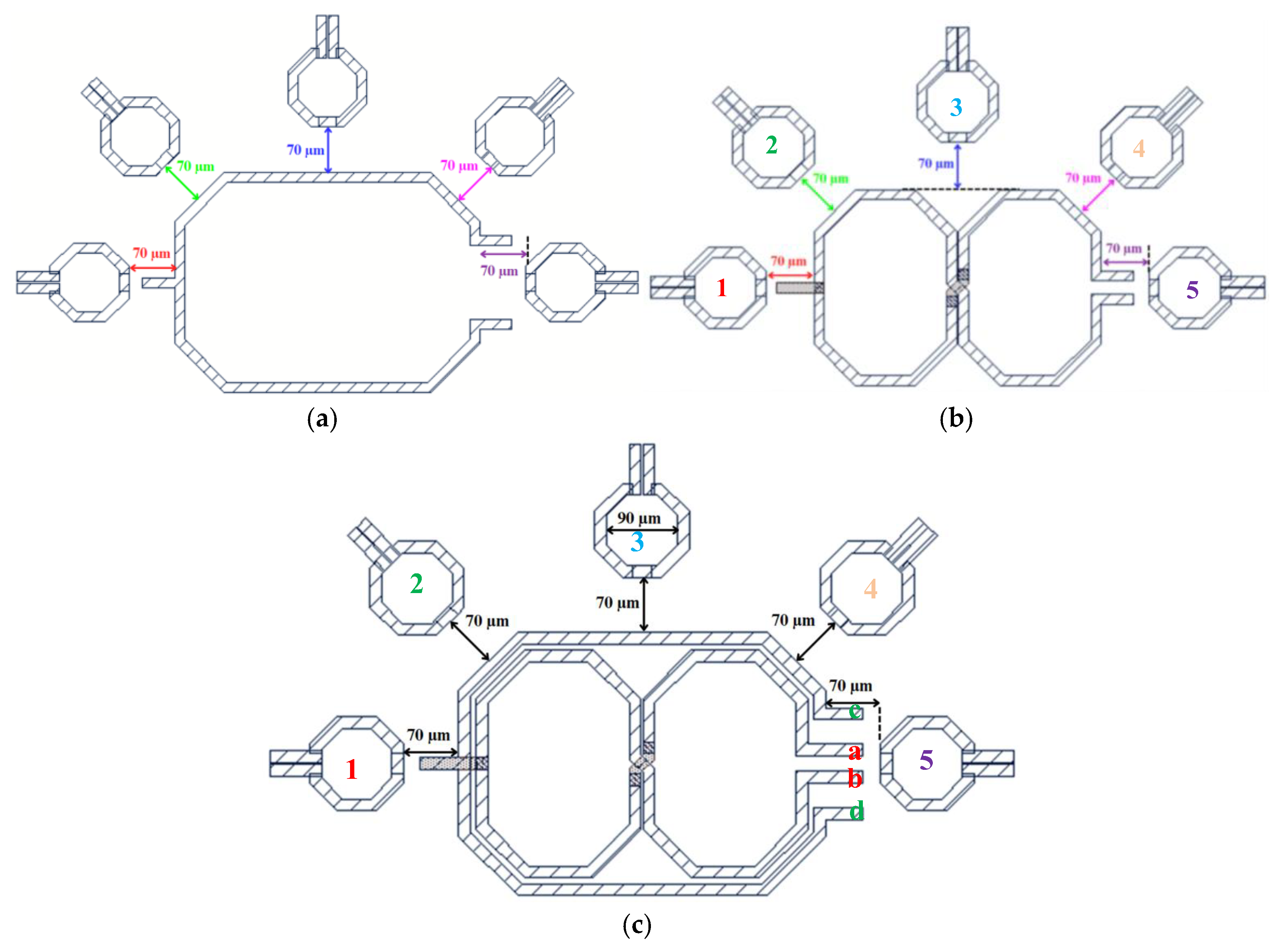
2.1. 1st Circuit Design
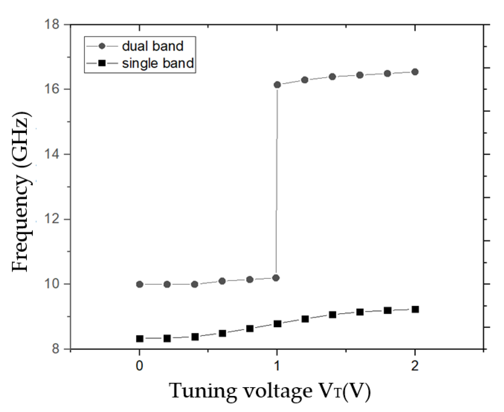
2.2. 2nd Circuit Design
3. Left-Hand Resonator VCO Using an Orthogonal Transformer
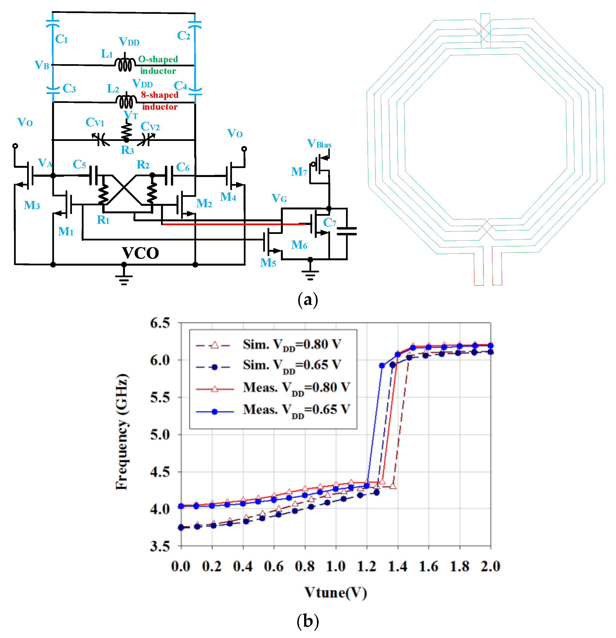
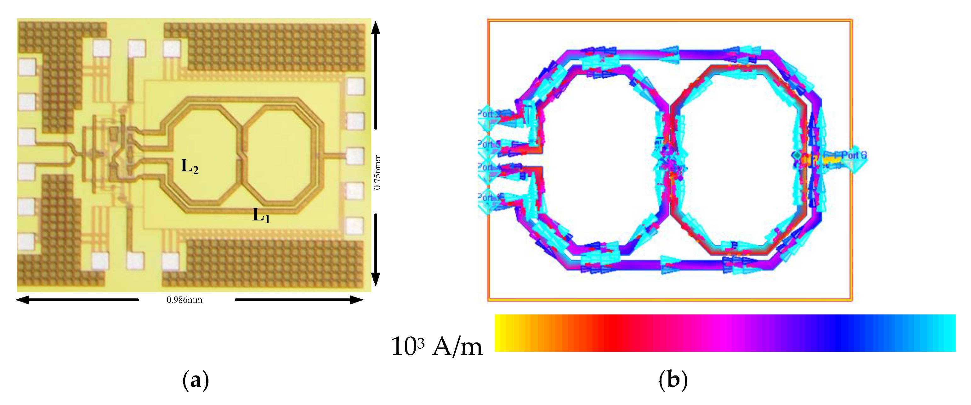
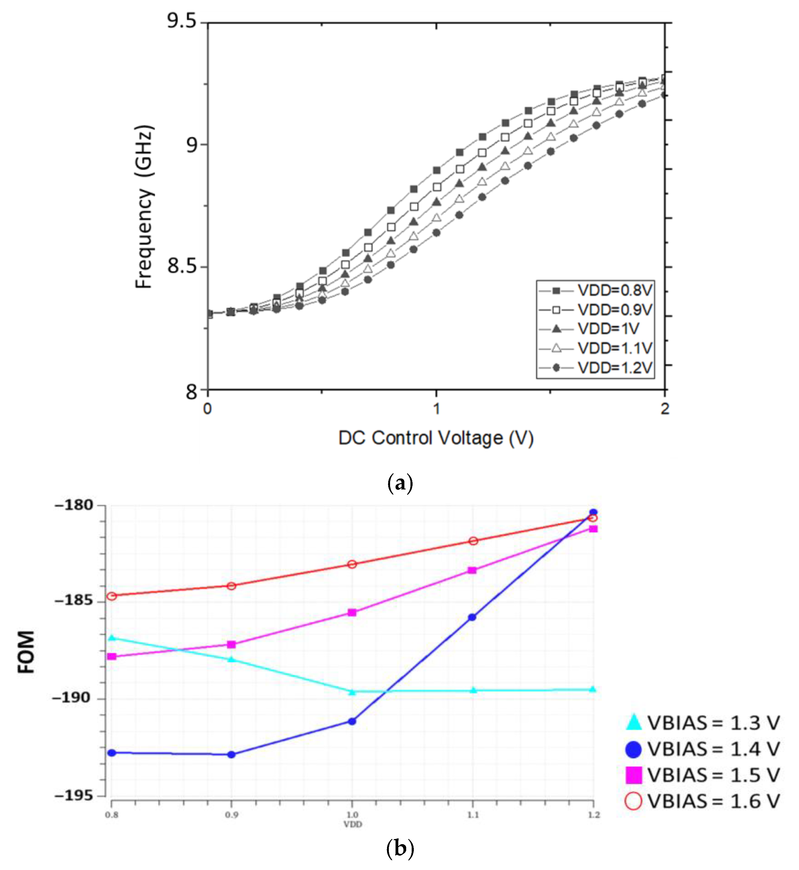
3.1. Circuit Design
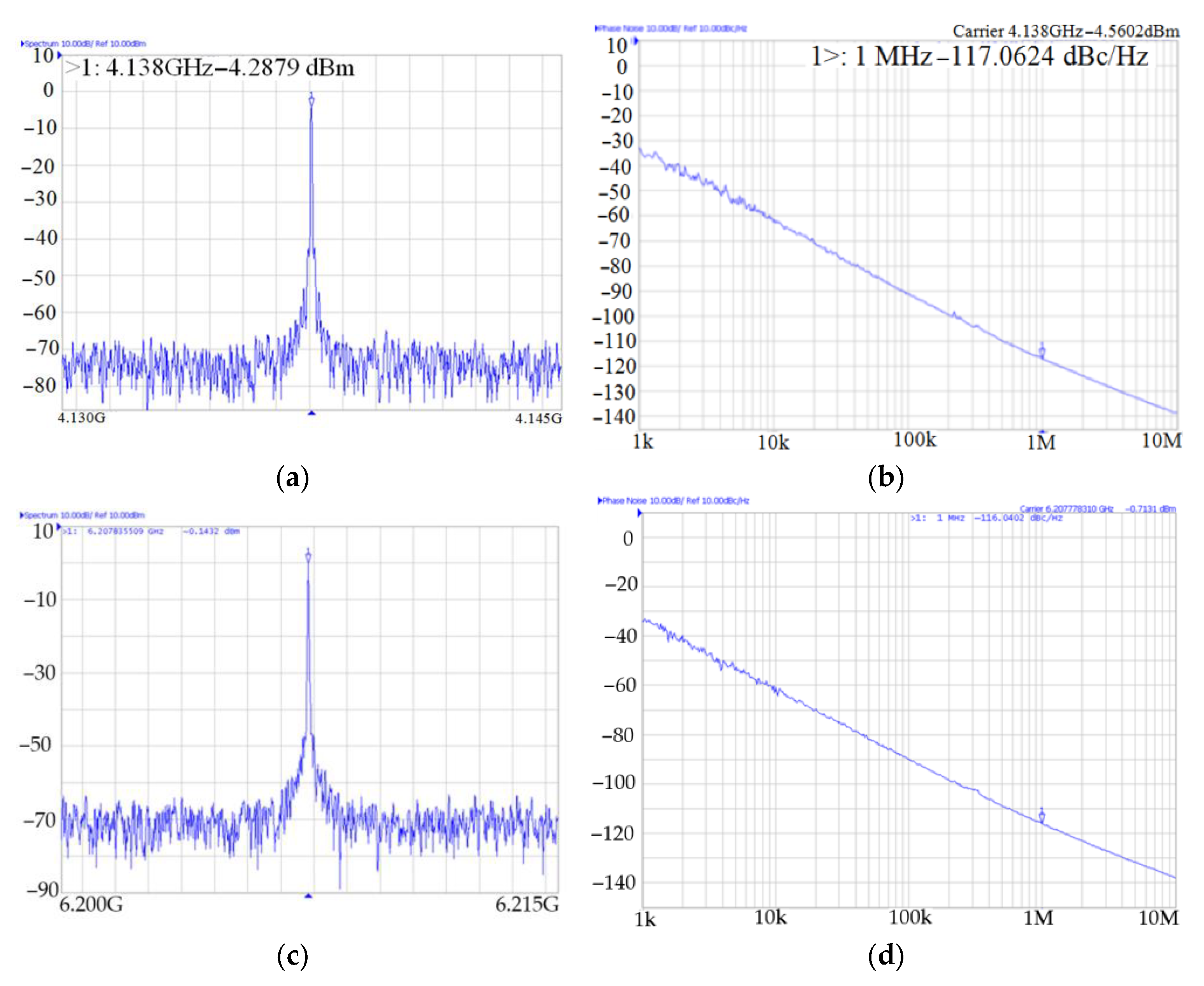
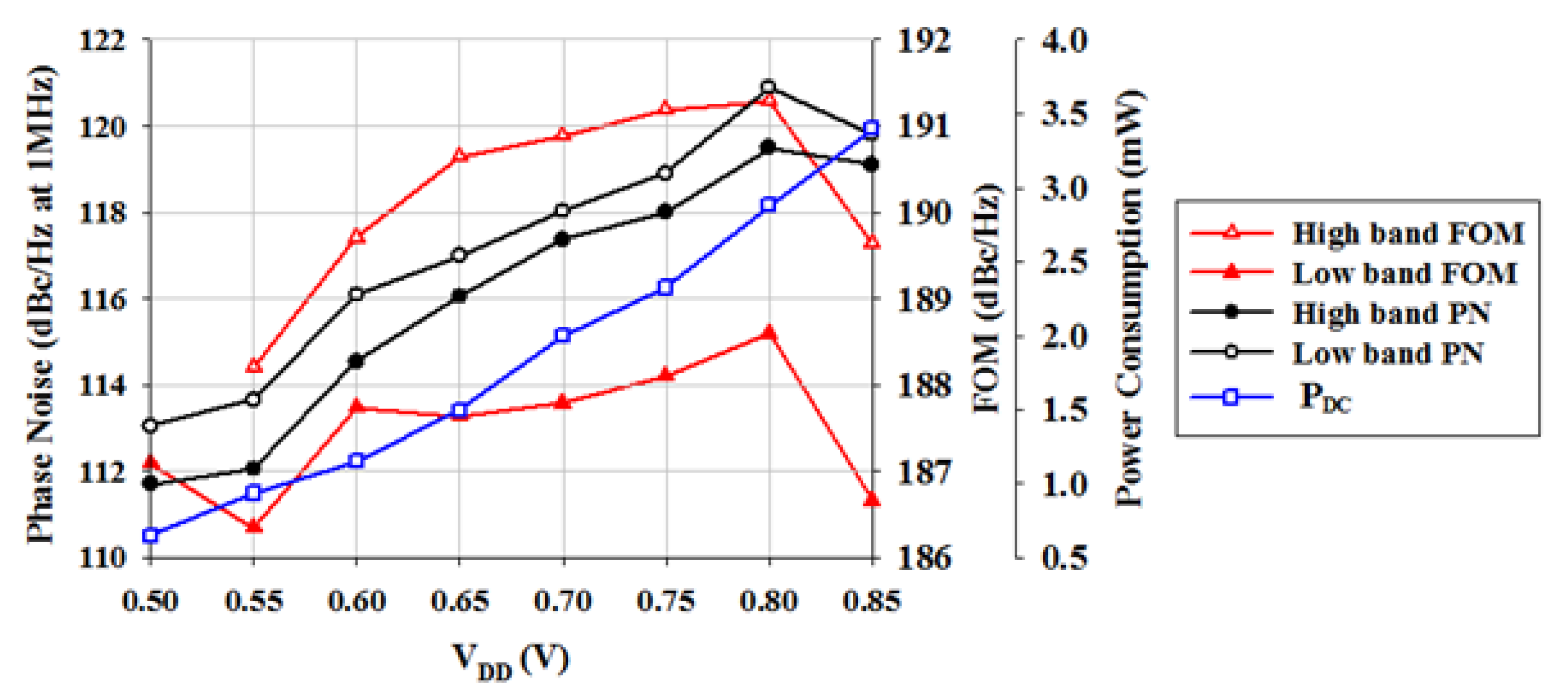
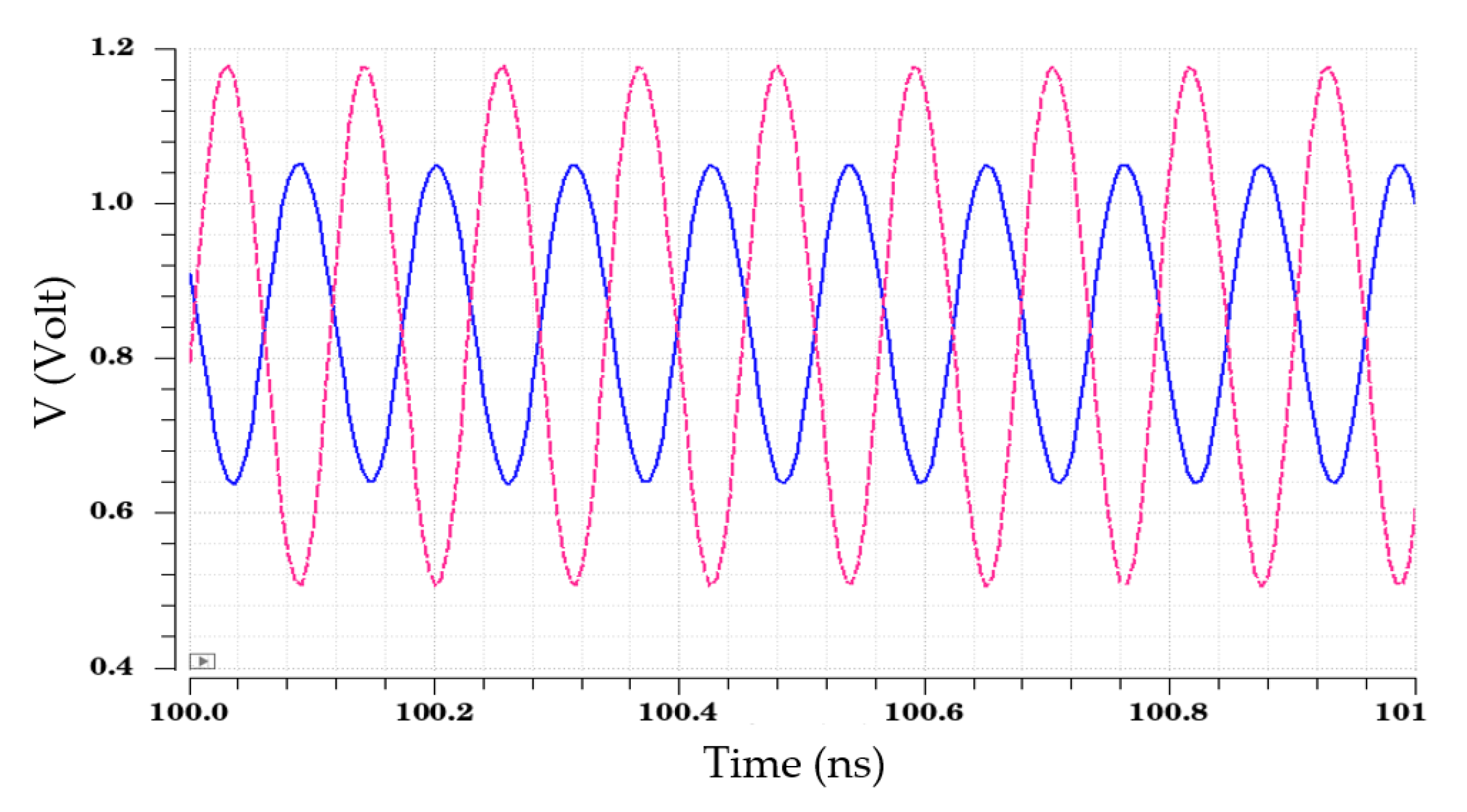
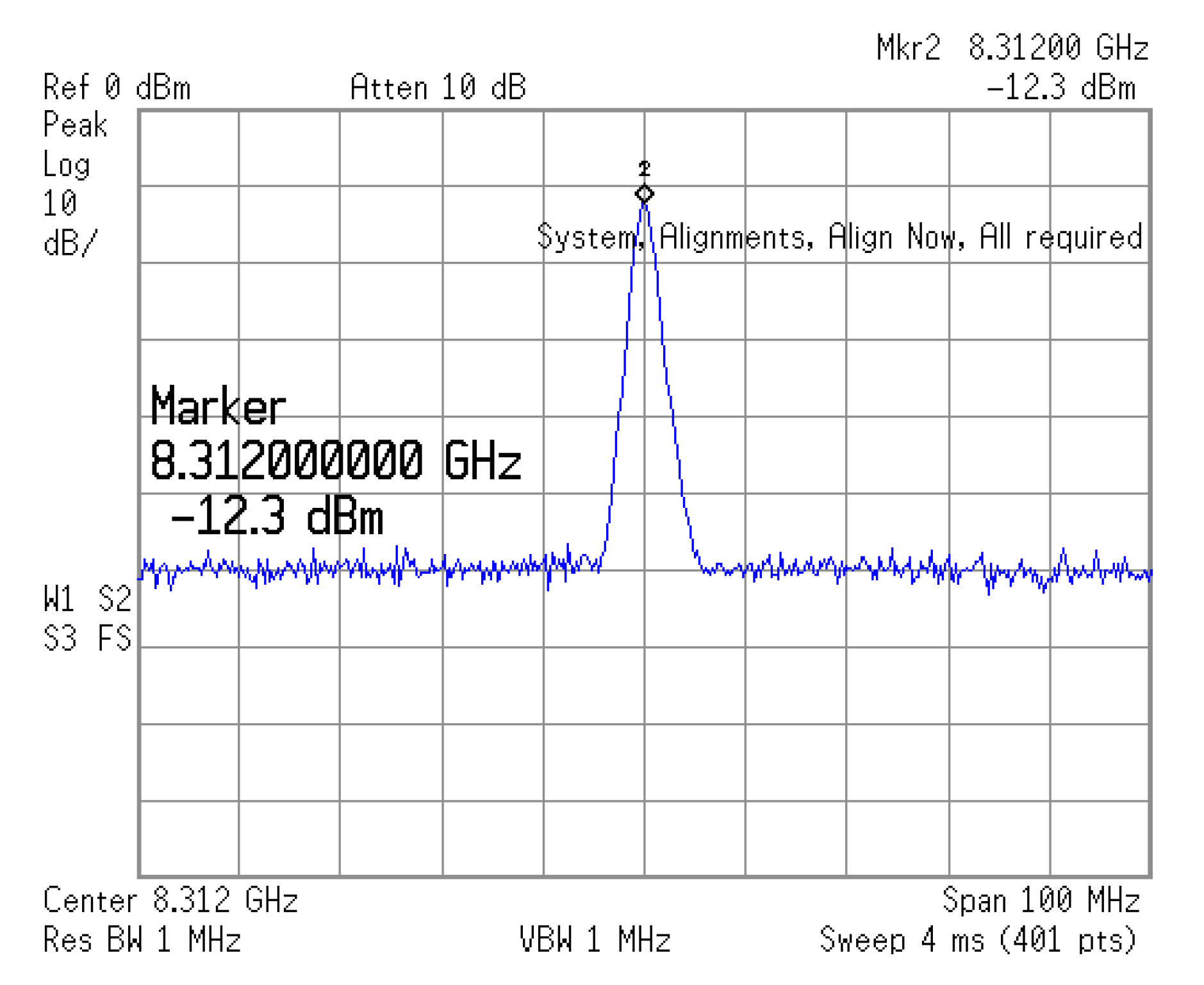
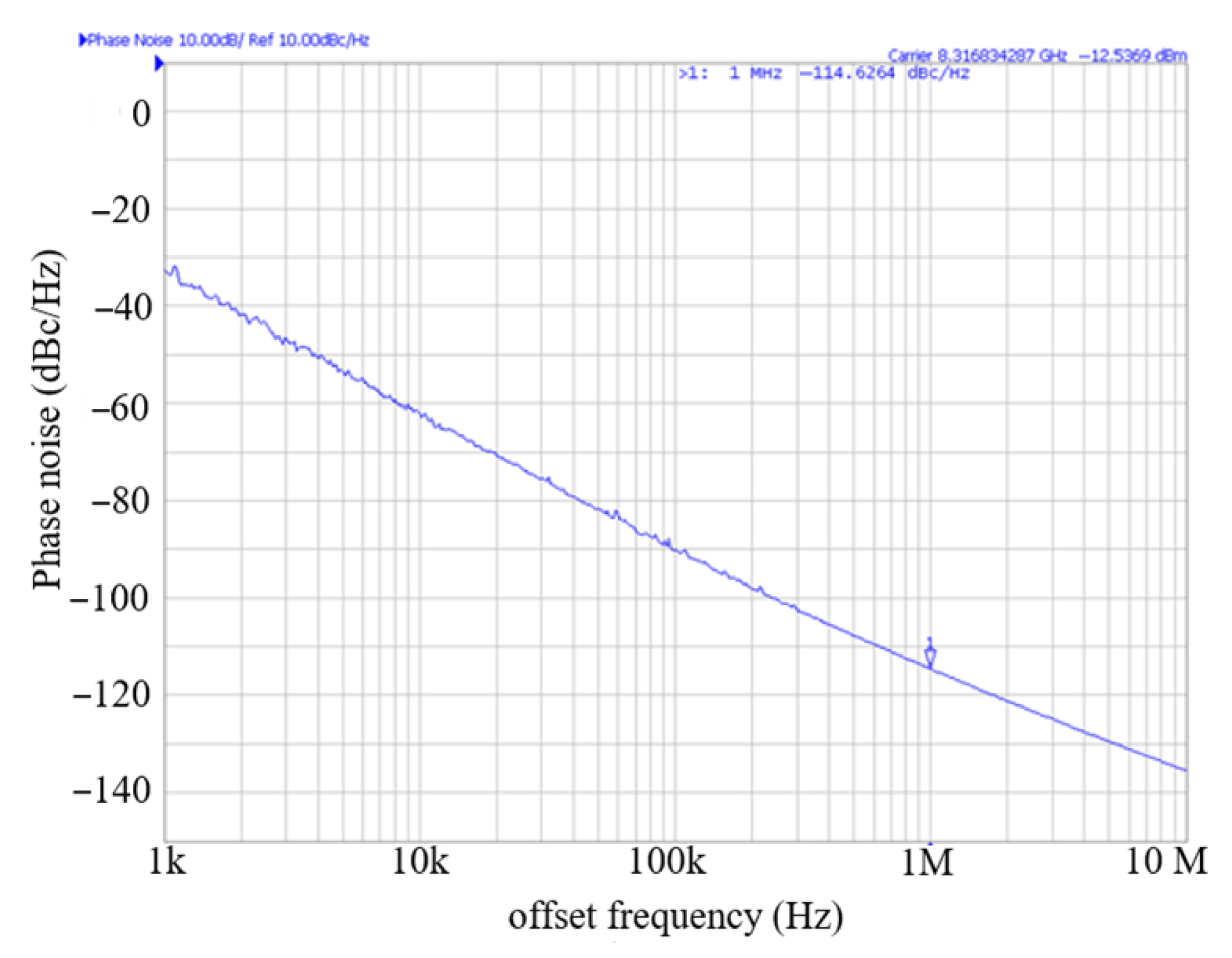
3.2. Experiment
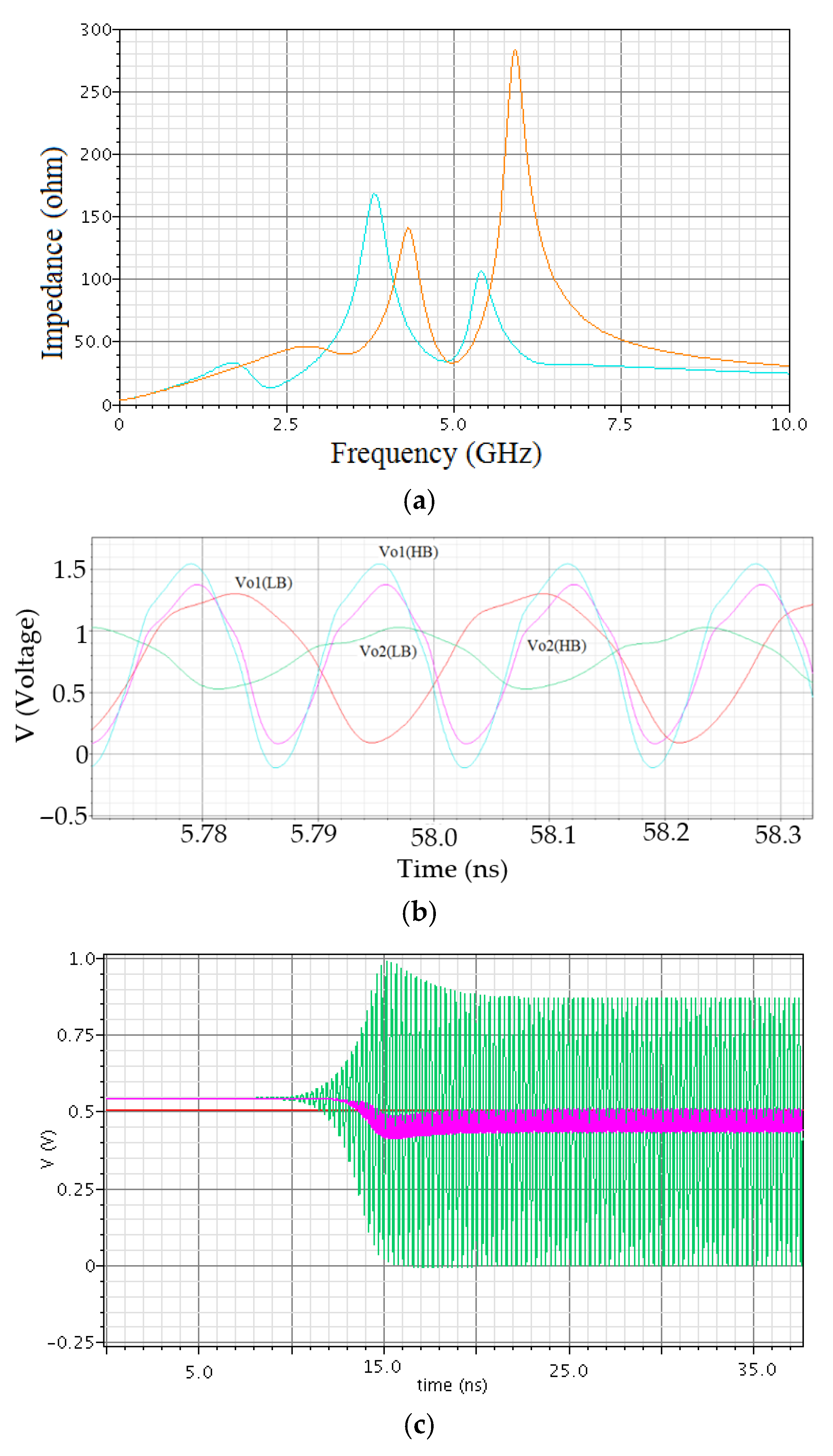
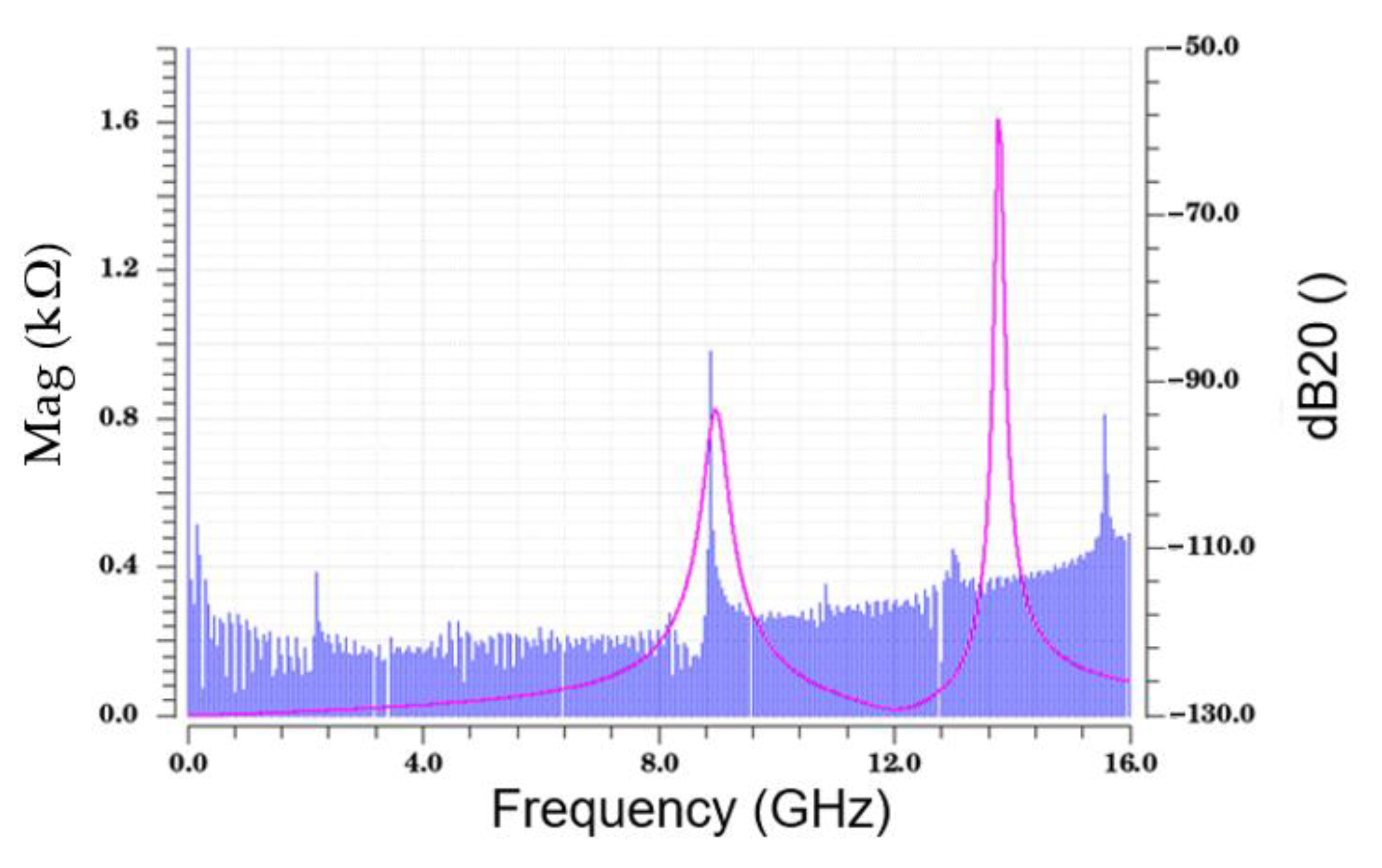
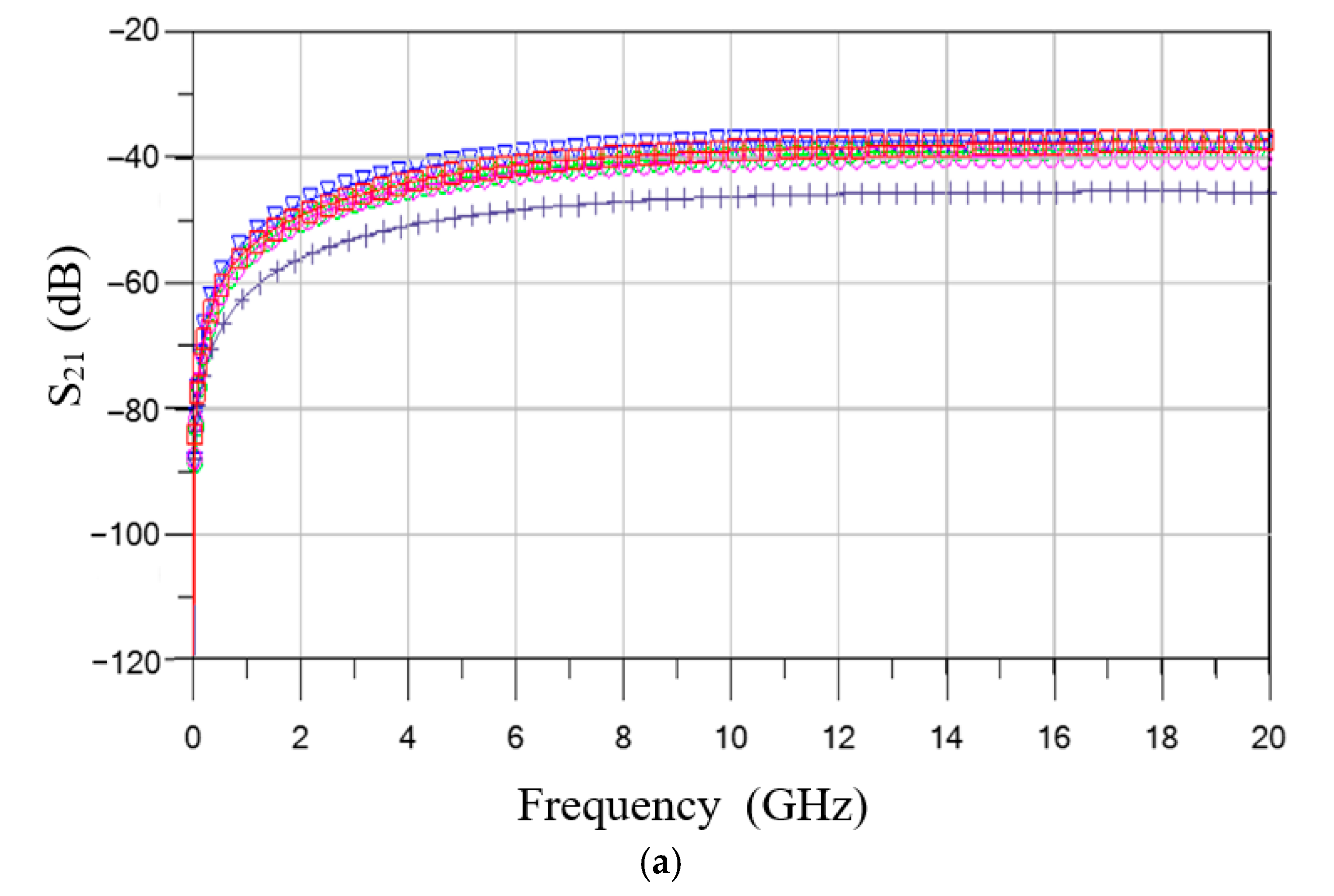
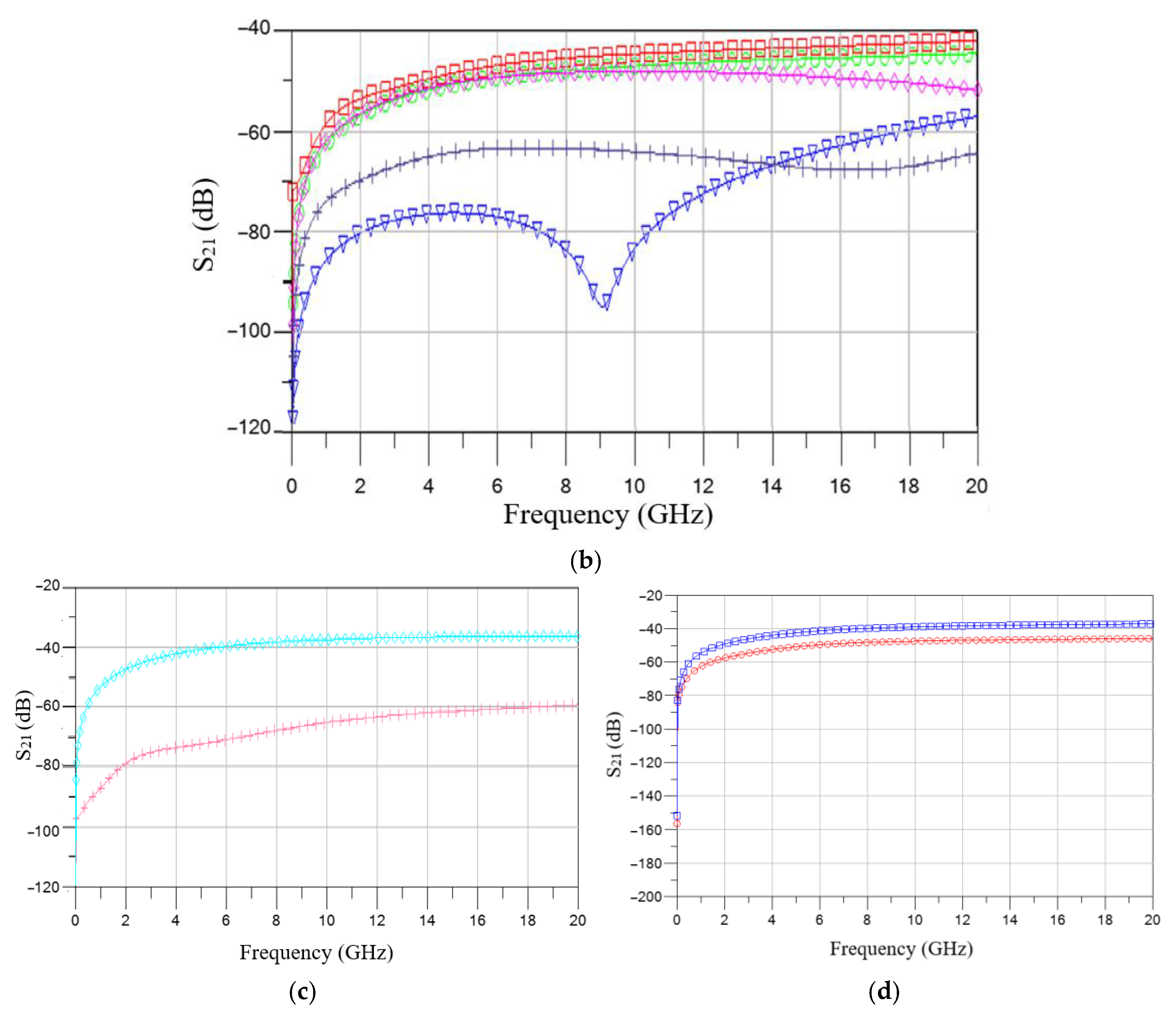
3.3. Coupling Noise Simulation
4. Conclusions
Author Contributions
Funding
Data Availability Statement
Acknowledgments
Conflicts of Interest
References
- Gagliardi, F.; Manfredini, G.; Ria, A.; Piotto, M.; Bruschi, P. Low-phase-noise CMOS relaxation oscillators for on-chip timing of IoT sensing platforms. Electronics 2022, 11, 1794. [Google Scholar] [CrossRef]
- Esmaeilzadeh, M.; Audet, Y.; Ali, M.; Sawan, M. A low-phase-noise CMOS ring voltage-controlled oscillator intended for time-based sensor interfaces. IEEE Access 2022, 10, 101186–101197. [Google Scholar] [CrossRef]
- Jang, S.-L.; Lin, Z.-J.; Juang, M.-H. State-of-the-Art VCO with eight-shaped resonator-type transmission line. Electronics 2025, 14, 2322. [Google Scholar] [CrossRef]
- Lai, A.; Caloz, C.; Itoh, T. Composite right/left-handed transmission line metamaterials. IEEE Microw. Mag. 2004, 5, 34–50. [Google Scholar]
- Gertman, I.; Levinger, R.; Bershansky, S.; Kadry, J.; Horovitz, G. A 33% tuning range cross-coupled DCO with “Folded” common mode resonator covering both 5G MMW bands in 16-nm CMOS FinFet. In Proceedings of the 2020 15th European Microwave Integrated Circuits Conference (EuMIC), Utrecht, The Netherlands, 11–12 January 2021; pp. 109–112. [Google Scholar]
- Jang, S.-L.; Dai, B.-R.; Lai, W.-C.; Juang, M.-H. Area-efficient standing-wave oscillator with a double-8-shaped inductor. In Proceedings of the 2023 Asia-Pacific Microwave Conference (APMC), Taipei, Taiwan, 5–8 December 2023; pp. 34–36. [Google Scholar] [CrossRef]
- Chang, C.F.; Itoh, T. A dual-band millimeter–wave CMOS oscillator with left-handed resonator. IEEE Trans. Microw. Theory Technol. 2010, 58, 1401–1409. [Google Scholar]
- Jang, S.-L.; Lai, W.-C.; Kung, T.-C. A low noise class-C voltage-controlled oscillator with left-handed resonator. In Proceedings of the 2016 5th International Symposium on Next-Generation Electronics (ISNE), Hsinchu, Taiwan, 4–6 May 2016; pp. 1–2. [Google Scholar] [CrossRef]
- Levantino, S.; Samori, C.; Bonfanti, A.; Gierkink, S.L.J.; Lacaita, A.L.; Boccuzzi, V. Frequency dependence on bias current in 5 GHz CMOS VCOs: Impact on tuning range and flicker noise upconversion. IEEE J. Solid-State Circuit 2002, 37, 1003–1011. [Google Scholar]
- Mohan, S.; del Mar Hershenson, M.; Boyd, S.P.; Lee, T.H. Simple accurate expressions for planar spiral inductances. IEEE J. Solid-State Circuits 1999, 34, 1419–1424. [Google Scholar]
- Lai, W.-C.; Jang, S.-L.; Shih, B.-S. A VCO with dynamic body injection and class-C technique. In Proceedings of the 2018 13th International Microsystems, Packaging, Assembly and Circuits Technology Conference (IMPACT), Taipei, Taiwan, 2 June 2018; pp. 226–229. [Google Scholar] [CrossRef]
- Ikeda, S.; Kamimura, T.; Lee, S.; Kanemaru, N.; Ito, H.; Ishihara, N.; Masu, K. A 0.5-V 5.5-GHz class-C-VCO-based PLL with ultra-low-power ILFO in 65 nm CMOS. In Proceedings of the 2012 IEEE Asian Solid State Circuits Conference (A-SSCC), Kobe, Japan, 12–14 November 2012; pp. 357–360. [Google Scholar] [CrossRef]
- Lai, W.-C.; Jang, S.-L.; Wang, J.-J. Dual-band quadrature VCO using switched-transformer coupling for wireless robot applications. In Proceedings of the 2019 4th Asia-Pacific Conference on Intelligent Robot Systems (ACIRS), Nagoya, Japan, 13–15 July 2019; pp. 109–112. [Google Scholar] [CrossRef]
- Jang, S.-L.; Lin, W.-C.; Sung, J.-Y.; Hsu, M.-H.; Lai, W.-C. Area-efficient and coupling noise suppressive voltage-controlled oscillator. In Proceedings of the 2024 IEEE Ultrasonics, Ferroelectrics, and Frequency Control Joint Symposium (UFFC-JS), Taipei, Taiwan, 22–26 September 2024; pp. 1–4. [Google Scholar] [CrossRef]
- Moroni, A.; Genesi, R.; Manstretta, D. Analysis and design of a 54 GHz distributed ‘hybrid’ wave oscillator array with quadrature outputs. IEEE J. Solid-State Circuits 2014, 49, 1158–1172. [Google Scholar]
- Nouri, N.; Buckwalter, J.F. A 45-GHz rotary-wave voltage-controlled oscillator. IEEE Trans. Microw. Theory Technol. 2011, 59, 83–392. [Google Scholar]
- Shehata, M.A.; Keaveney, M.; Staszewski, R.B. A 184.6-dBc/Hz FoM 100-kHz flicker phase noise corner 30-GHz rotary traveling-wave oscillator using distributed stubs in 22-nm FD-SOI. IEEE Solid-State Circuits Lett. 2019, 2, 103–106. [Google Scholar] [CrossRef]
- Ansari, K.T.; Ross, T.; Gamand, P.; Plett, C. Frequency domain phase shift measurement technique applied to a multiphase rotary travelling-wave VCO. IEEE Microw. Compon. Lett. 2015, 25, 820–822. [Google Scholar] [CrossRef]
- Peng, Y.Y.; Yu, X.P.; Gu, J.M.; Lim, W.M.; Sui, W.Q. An area efficient CRLH (Composite Right/Left-Handed)-TL approach to the design of rotary traveling-wave oscillator. IEEE Microw. Wireless Compon. Lett. 2013, 23, 560–562. [Google Scholar] [CrossRef]
- Lai, W.-C.; Jang, S.-L.; Syu, J.-W. Quadrature VCO via transformer-coupled transmission line. In Proceedings of the 2019 12th International Workshop on the Electromagnetic Compatibility of Integrated Circuits (EMC Compo), Hangzhou, China, 21–23 October 2019; pp. 2–5. [Google Scholar] [CrossRef]
- Yim, S.M.; O, K.K. Switched resonators and their applications in a dual-band monolithic CMOS LC-tuned VCO. IEEE Trans. Microw. Theory Technol. 2006, 54, 74–81. [Google Scholar]
- Zhang, J.; Sharma, N.; Kenneth, K.O. 21.5-to-33.4 GHz voltage-controlled oscillator using NMOS switched inductors in CMOS. IEEE Microw. Wireless Compon. Lett. 2014, 24, 478–480. [Google Scholar]
- Peng, Y.; Zhou, L.; Yu, Y.; Liu, H.; Wu, Y.; Zhao, C.; Tang, H.; Kang, K. A harmonic-tuned VCO with an intrinsic-high-Q F23 inductor in 65-nm CMOS. IEEE Microw. Wireless Compon. Lett. 2020, 30, 981–984. [Google Scholar] [CrossRef]


| Ref. | CMOS Process (um) | Topology Used | VDD (V) | fo (GHz) | Pdiss. (mW) | Tuning Range GHz, (%) | Area (mm2) | PNoise @1 MHz (dBc/Hz) | FOM, (dBc/Hz) |
|---|---|---|---|---|---|---|---|---|---|
| [3] June 2025 | 0.18 | RTWO | 1.7 | 8.53 | 5.8 | 8.53~10 | 1.2 × 1.2 | −122.4 | −193.4 |
| [6] December 2023 | 0.18 | RH-SWO | 1.2 | 9.94 | 4.3 | 0 | 0.947 × 0.8 | −115.07 | −188.59 |
| [7] May 2010 | 0.13 | LH-CRHL | - | 21/55 | 14 | 21/55 | 0.15 × 0.06 (core) | −100.8/−86.7 | −175.8/−170.2 |
| [13] July 2019 | 0.18 | RTWO | 1.3 | 2.84~3.44 | 7.52 | 19.10 | 1.2 × 1.2 | −113.9 | −173.8 |
| 1.1 | 2.41~2.8 | 4.78 | 14.97 | −121.4 | −181.8 | ||||
| [14] October 2024 | 0.18 | NP-Cross | 1.7 | 6.979 | 3.875 | 6.88~6.1 | 0.83 × 0.78 | −119.32 | −189.86 |
| [15] May 2014 | 0.065 | Hybrid RTWO | 1.2 | 51.9 | 36 | 8.5 | - | −86.0 | −164.7 |
| [16] February 2011 | 0.12 | Hybrid RTWO | 1.2 | 45.0 | 19.2 | 6.5 | 0.5 × 0.5 | −93.0 | −173.2 |
| [17] September 2019 | 0.022 | RTWO | 0.8 | 26.2 | 21 | 13.5 | 0.115 × 0.115 | −109.2 | −184.2 |
| [18] December 2015 | 0.125Bi | RTWO | - | 15.0 | 52 | 1.65 | - | −112.2 | −178.56 |
| [19] October 2013 | 0.18 | CRLH TL | 1.8 | 23.6 | 70.2 | - | 0.8 | −105 | - |
| [20] October 2019 | 0.18 | RTWO | 1 | 3.26~3.98 | 5.33 | 19.89 | 1.07 × 1.07 | −122.143 | −185.11 |
| [21] January 2006 | 0.18 | Switch resonator | 1.8 | 0.865 | 16 | 13 | 0.69 × 1.3 | −125@600 K | −176 |
| 1.812 | 24 | −123@600 K | −181 | ||||||
| [22] July 2014 | 0.065 | Swit res | 27.5 | 4.8 | 43.3 | 0.084 | −90 | −171.97 | |
| [23] December 2020 | 0.065 | Cross-co | 0.55 | 6.8 | 5 | 12 | 0.3 × 0.7 | −117.5 | −187.2 |
| This 1 2013 | 0.18 | LH-SWO | 0.8 | 3.858 6.22 | 3.11 | 3.85~4.29 6.06~6.37 | 0.435 × 0.809 | −120.01 −120.17 | −187.0 −191.0 |
| This 2 2016 | 0.18 | LH-SWO | 0.65 | 4.138 6.207 | 1.495 | 4.138 6.207 | 0.527 × 0.749 | −117.06 −116.04 | −187.64 −190.15 |
| This work 3 | 0.18 | LH-SWO | 0.9 | 9.23(Vbias = 1.4 V) | 2.07 | 10.83 | 0.986 × 0.756 | −109.54 | −185.8 |
| This work 3 | 0.18 | LH-SWO | 0.9 | 8.3(Vbias = 1.7 V) | 3.1 | 10.83 | 0.986 × 0.756 | −114.6 | −188.6 |
Disclaimer/Publisher’s Note: The statements, opinions and data contained in all publications are solely those of the individual author(s) and contributor(s) and not of MDPI and/or the editor(s). MDPI and/or the editor(s) disclaim responsibility for any injury to people or property resulting from any ideas, methods, instructions or products referred to in the content. |
© 2025 by the authors. Licensee MDPI, Basel, Switzerland. This article is an open access article distributed under the terms and conditions of the Creative Commons Attribution (CC BY) license (https://creativecommons.org/licenses/by/4.0/).
Share and Cite
Jang, S.-L.; Lee, Y.-C.; Lai, W.-C. Left-Hand Resonator VCO Using an Orthogonal Transformer. Electronics 2025, 14, 2765. https://doi.org/10.3390/electronics14142765
Jang S-L, Lee Y-C, Lai W-C. Left-Hand Resonator VCO Using an Orthogonal Transformer. Electronics. 2025; 14(14):2765. https://doi.org/10.3390/electronics14142765
Chicago/Turabian StyleJang, Sheng-Lyang, Yun-Chien Lee, and Wen-Cheng Lai. 2025. "Left-Hand Resonator VCO Using an Orthogonal Transformer" Electronics 14, no. 14: 2765. https://doi.org/10.3390/electronics14142765
APA StyleJang, S.-L., Lee, Y.-C., & Lai, W.-C. (2025). Left-Hand Resonator VCO Using an Orthogonal Transformer. Electronics, 14(14), 2765. https://doi.org/10.3390/electronics14142765