Article

Highly Linear 2.6 GHz Band InGaP/GaAs HBT Power Amplifier IC Using a Dynamic Predistorter

by
Hyeongjin Jeon
1,2,
Jaekyung Shin
3,
Woojin Choi
3,
Sooncheol Bae
1,
Kyungdong Bae
1,2,
Soohyun Bin
1,
Sangyeop Kim
1,
Yunhyung Ju
1,
Minseok Ahn
1,
Gyuhyeon Mun
1,
Keum Cheol Hwang
1,
Kang-Yoon Lee
1 and
Youngoo Yang
1,2,*
1
Department of Electrical and Computer Engineering, Sungkyunkwan University, 2066 Seobu-ro, Jangan-gu, Suwon-si 16419, Gyeonggi-do, Republic of Korea
2
para-PA Inc., 2066 Seobu-ro, Jangan-gu, Suwon-si 16419, Gyeonggi-do, Republic of Korea
3
Samsung Electronics Co., Ltd., 129 Samsung-ro, Yeongtong-gu, Suwon-si 16677, Gyeonggi-do, Republic of Korea
*
Author to whom correspondence should be addressed.
Electronics 2025, 14(11), 2300; https://doi.org/10.3390/electronics14112300
Submission received: 15 May 2025 / Revised: 1 June 2025 / Accepted: 2 June 2025 / Published: 5 June 2025
(This article belongs to the Section Microwave and Wireless Communications)

Abstract

:
This paper presents a highly linear two-stage InGaP/GaAs power amplifier integrated circuit (PAIC) using a dynamic predistorter for 5G small-cell applications. The proposed predistorter, based on a diode-connected transistor, utilizes a supply voltage to accurately control the linearization characteristics by adjusting its dc current. It is connected in parallel with an inter-stage of the two-stage PAIC through a series configuration of a resistor and an inductor, and features a shunt capacitor at the base of the transistor. These passive components have been optimized to enhance the linearization performance by managing the RF signal’s coupling to the diode. Using these optimized components, the AM−AM and AM−PM nonlinearities arising from the nonlinear resistance and capacitance in the diode can be effectively used to significantly flatten the AM−AM and AM−PM characteristics of the PAIC. The proposed predistorter was applied to the 2.6 GHz two-stage InGaP/GaAs HBT PAIC. The IC was tested using a 5 × 5 mm2 module package based on a four-layer laminate. The load network was implemented off-chip on the laminate. By employing a continuous-wave (CW) signal, the AM−AM and AM−PM characteristics at 2.55–2.65 GHz were improved by approximately 0.05 dB and 3°, respectively. When utilizing the new radio (NR) signal, based on OFDM cyclic prefix (CP) with a signal bandwidth of 100 MHz and a peak-to-average power ratio (PAPR) of 9.7 dB, the power-added efficiency (PAE) reached at least 11.8%, and the average output power was no less than 24 dBm, achieving an adjacent channel leakage power ratio (ACLR) of −40.0 dBc.

1. Introduction

In recent years, as wireless communication systems have advanced, the need for higher data rates and more efficient management of increasing mobile traffic has become crucial. Small cells, designed to provide reliable coverage in confined areas, are now densely deployed to achieve high spatial and spectral efficiency at increased data rates, making them an essential component in 5G and future wireless networks [1]. For these networks, orthogonal frequency division multiplexing (OFDM) is utilized for both uplink and downlink communications. The OFDM-based modulated signal, characterized by high PAPR, imposes stringent linearity requirements on PAs, especially in small-cell applications [2].
Additionally, the PA consumes a significant amount of power; hence, high efficiency is crucial. To enhance power efficiency, PAs with low quiescent current such as class-AB have been utilized [3,4]. However, operating with low quiescent current may lead to nonlinear distortion in both AM−AM and AM−PM. To achieve the required linearity specifications, particularly for modulated signals with high PAPR, the PA operates in a large Output Power Back-Off (OBO) region. As OBO increases to improve linearity, the PAE decreases. Consequently, there is a need for research into linearization techniques for small-cell PAs with low quiescent current to enable more efficient operations.
Accordingly, various linearization techniques have been investigated, and external approaches such as digital predistortion (DPD) and analog predistortion (APD) have been widely applied [5,6,7,8,9]. While DPD has become the mainstream solution in recent years, it requires high-speed data converters, complex digital signal processing, and significant power consumption, which may limit its applicability in compact and low-power systems. In contrast, APD offers several advantages, including lower power consumption, real-time operation without latency, and simplified hardware implementation. The APD techniques include feedback [5], feedforward [6], and predistortion [7,8,9]. The feedback technique offers advantages in linearity and stability but results in reduced gain. Feedforward linearization achieves significant improvements in linearity but requires an additional error amplifier, complicating its integration as an IC. Predistortion linearization typically provides moderate linearity enhancements at a relatively low additional cost and benefits from its compact size, low complexity, and enhanced stability. As depicted in Figure 1, predistortion linearization operates by flattening the overall AM−AM and AM−PM characteristics through a predistorter, which possesses characteristics opposite to those of a nonlinear PA. Consequently, this results in linear signal amplification at the output.
Generally, since PAs tend to exhibit gain compression characteristics, designing a predistorter with gain expansion characteristics is necessary to counteract the PA’s gain compression [7,8,9]. However, when PAs operate with low quiescent current to boost efficiency, they exhibit a more dynamic response in their amplitude response (AM−AM) where gain expansion appears before gain compression. A similar dynamic is noticeable in the phase response (AM−PM). Specifically, the InGaP/GaAs HBT PA displays dynamic nonlinear characteristics that vary based on the configuration of its active bias circuits [3,4]. The AM−PM characteristics also change depending on the harmonic impedance at the matching network and the active bias circuits. Therefore, a predistorter capable of compensating for these dynamic AM−AM and AM−PM characteristics of the InGaP/GaAs HBT PA is essential.
This paper proposes a predistorter that dynamically compensates for the nonlinear characteristics of the two-stage InGaP/GaAs HBT PAIC used in 5G small-cell applications. It comprises a diode-connected transistor, a shunt capacitor at the base, and a series-connected inductor and resistor that link the emitter to the inter-stage matching network in parallel. These passive components optimize the RF signal coupling to the diode, which significantly influences the nonlinear characteristics of the predistorter. Furthermore, the nonlinear behavior of the proposed predistorter can be controlled by supplying a dc current to its base collector. Through the integration of these control mechanisms, the predistorter’s nonlinearity can dynamically respond to varying input power levels. The performance is evaluated before and after applying predistortion linearization by measuring the fabricated PAIC using both CW and modulated signals.

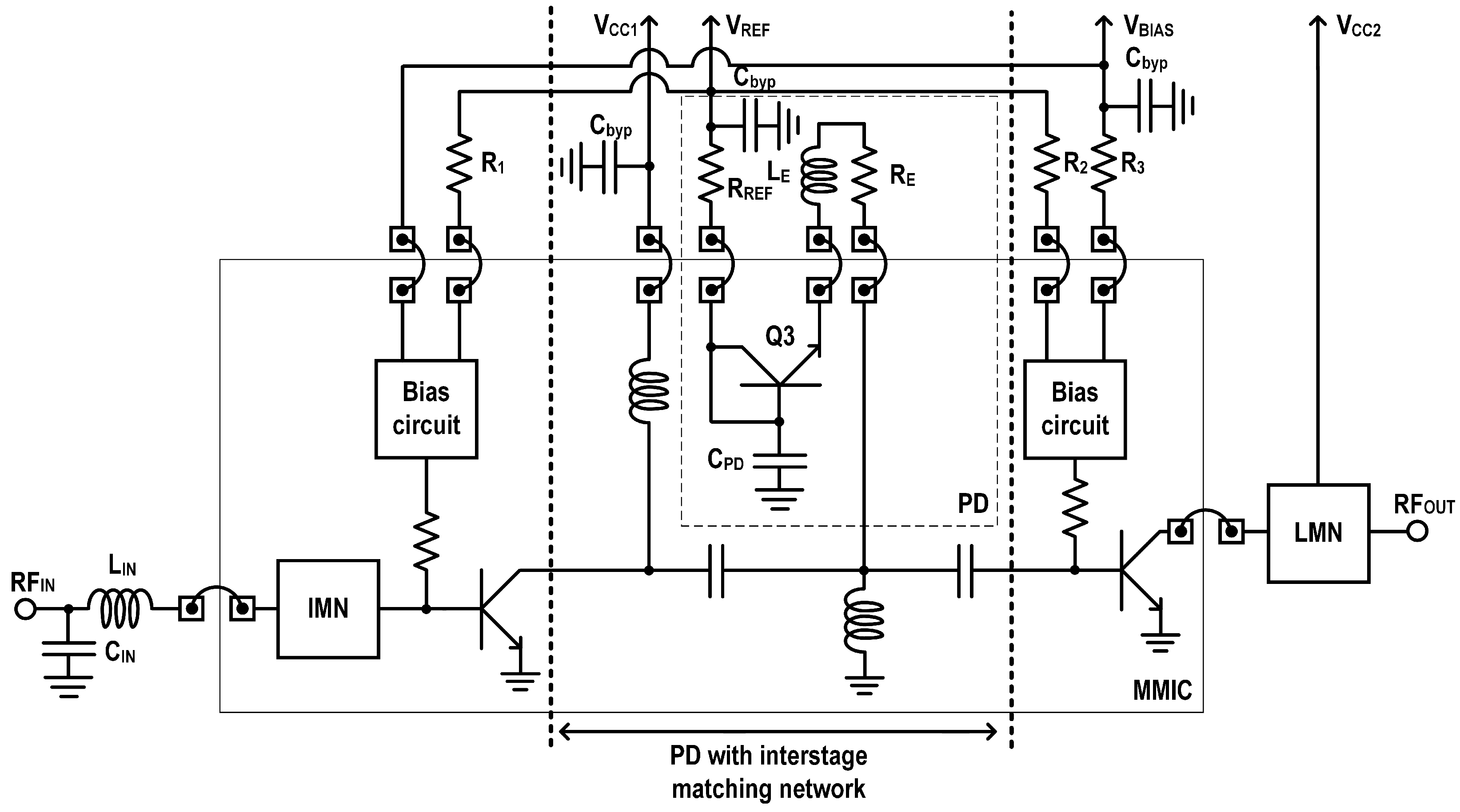
2. Design of the Dynamic Predistorter

2.1. Circuit Configuration

The conventional shunt diode predistorter depicted in Figure 2a uses a biased diode connected in parallel to the RF signal path with a series capacitor ( C o p t ) [9]. C o p t directly affects the RF power coupling to the predistorter. The voltage distribution across the predistorter is divided between the diode and C o p t . The nonlinearity of the diode is represented by a nonlinear resistance, R d i o d e , which is adjustable through the reference voltage ( V R E F ). Thus, the conventional predistorter, with two parameters ( C o p t and V R E F ), offers limited control over its ability to compensate for the dynamic nonlinear characteristics of PAs.
The proposed dynamic predistorter, illustrated in Figure 2b, utilizes a suitably biased diode-connected bipolar transistor (Q3). It is connected in parallel to the RF signal path at the inter-stage matching network via a series resistor ( R E ) and inductor ( L E ). A shunt capacitor ( C P D ) is added at the base of Q3 to provide degeneration to Q3. The degeneration capacitance, C P D , works with the diode, R E , and L E to divide the voltage [10]. R E and L E primarily regulate the signal coupling from the RF signal path. The voltage across the proposed predistorter is then split among the diode, C P D , R E , and L E . The proposed predistorter features additional control parameters such as C P D , V R E F , R E , and L E , which influence the overall nonlinearities generated by the predistorter and enhance the capability to compensate for dynamic nonlinear characteristics across a wide power range of the PA.

2.2. Dynamic Compensation of Nonlinearities

Figure 3 illustrates the simulated AM−AM and AM−PM characteristics of the predistorter based on various tuning parameter values, such as C P D , V R E F , R E , and L E . Figure 3a depicts the AM−AM and AM−PM characteristics for five distinct values of C P D with a V R E F of 3.1 V, R R E F of 300 Ω , L E of 3 nH, and R E of 15 Ω . As C P D decreases, capacitive degeneration intensifies, leading to a significant increase in AM−PM variation. Particularly for values above 3 pF, the AM−PM variation becomes pronounced, while the AM−AM characteristics show limited change with dynamic responses involving compression and expansion. Figure 3b demonstrates the AM−AM and AM−PM performance for five varying values of V R E F with an R R E F of 300 Ω , a C P D of 5 pF, an L E of 3 nH, and an R E of 15 Ω . As V R E F decreases, the predistorter facilitates earlier and more pronounced variations in both AM−AM and AM−PM characteristics. Figure 3c showcases the AM−AM and AM−PM performance for five different values of L E with a V R E F of 3.1 V, an R R E F of 300 Ω , a C P D of 5 pF, and an R E of 15 Ω . Smaller L E values lead to greater RF signal coupling to the diode, which amplifies both the variation and dynamism in the AM−AM and AM−PM characteristics. For high L E values, the AM−PM characteristics tend to expand further. Figure 3d displays the AM−AM and AM−PM characteristics for five different values of R E with a V R E F of 3.1 V, an R R E F of 300 Ω , a C P D of 5 pF, and an L E of 3 nH. Smaller R E values enhance RF signal coupling to the diode, inducing greater variation across a relatively higher-input power spectrum.
The proposed predistorter is integrated into a two-stage PA employing an InGaP/GaAs HBT process, depicted in Figure 4. The emitter areas of the driver and main stages are 1440 and 5400 μm2, respectively. Active bias circuits, which supply current to the transistor’s base, are implemented in both the driver and main stages. The inter-stage matching network consists of two high-pass L-section circuits, incorporating a shunt inductor to provide both impedance matching and a DC current path for the predistorter. The predistorter, connected in parallel at the inter-stage matching network, minimally influences the impedance matching. The emitter area of Q3 measures 120 μm2.
Figure 5a demonstrates the simulated AM−AM and AM−PM characteristics of the two-stage HBT PAIC before and after the inclusion of the proposed dynamic predistorter. The predistorter’s tuning parameters were optimized to achieve optimal AM−AM and AM−PM compensation with a V R E F of 3.1 V, R R E F of 300 Ω , C P D of 5 pF, L E of 3 nH, and R E of 15 Ω . After applying the predistorter, noteworthy improvements in both the AM−AM and AM−PM characteristics were observed, effectively mitigating both the expansion and compression in the AM−AM characteristics and the significant expansion in the AM−PM characteristics. Specifically, the AM−AM improved by approximately 0.43 dB, while the AM−PM improved by about 4.7°. The ACLR, using the 5G NR signal based on QPSK CP-OFDM with a high PAPR of 9.7 dB, was enhanced by about 10 dB at an average output power of 24 dBm, as illustrated in Figure 5b.

3. Implementation and Measurement Results

Figure 6a displays a photograph of the implemented PAIC measuring 1.2 × 1.1 mm2, employing Winsemiconductor’s 2 μm InGaP/GaAs HBT process. Figure 6b shows a photograph of the module measuring 5 × 5 mm2 using a four-layer laminate. The diode-connected transistor and the shunt capacitor for the predistorter are integrated, whereas the R E and L E are external for tuning. The output-matching network consists of bond wires, surface-mount capacitors, and lines on the laminate. A V R E F of 3.1 V is supplied to the active bias circuits for both the driver and main stage.
Figure 7 shows the measured gain and PAE of the implemented PAIC with and without the predistorter using a CW signal. After applying the predistorter, the PAIC exhibited a gain of approximately 26.5–27.1 dB and a PAE of about 53% at an output power of 35 dBm across the 2.5–2.7 GHz frequency range. Compared to the case without the predistorter, a gain reduction of approximately 0.5 dB and an efficiency degradation of around 0.5% were observed. Figure 8 displays the measured AM−AM and AM−PM characteristics of the implemented PAIC with and without the predistorter using a CW signal at 2.55 GHz in Figure 8a and 2.65 GHz in Figure 8b. With the predistorter for both frequencies, it is observed that the saturated output power is extended by approximately 0.05 dB according to the AM−AM characteristics. These characteristics appear noticeably flatter. The AM−PM characteristics also demonstrate an improvement of more than 3°.
Figure 9 illustrates the measured performances of the PAIC for the carrier frequencies of 2.55–2.65 GHz using a 5G NR QPSK CP-OFDM signal with 273 RBs and a signal bandwidth of 100 MHz. Figure 9a presents the gain and PAE, while Figure 9b outlines the ACLR with and without the predistorter. At an average output power of 24.0 dBm, an ACLR below −40.0 dBc was achieved with the predistorter, compared to approximately −34.4 dBc without it. The gain and PAE at an average power of 24 dBm were recorded as 26.5–27.1 dB and 11.8%, respectively. The measurement results of this study are summarized in Table 1. Compared to previous works, this study demonstrates exceptional ACLR performance using a modulated signal with a wide signal bandwidth of 100 MHz and a high PAPR of 9.7 dB. The relatively low PAE is primarily attributed to the significantly large OBO of 11 dB.

4. Conclusions

In this paper, a highly linear two-stage InGaP/GaAs PAIC using a dynamic predistorter was proposed for 5G small-cell applications. The proposed predistorter is based on a diode-connected transistor placed in parallel at the inter-stage network. The AM−AM and AM−PM characteristics of the predistorter can be dynamically controlled and optimized to effectively compensate for the nonlinearities of the two-stage PA by adjusting the supply voltage to the diode and the passive elements surrounding the diode, such as a shunt capacitor at the base for degeneration and a series resistor and inductor at the emitter to couple the signal. Simulated dynamic characteristics were presented with various control parameter values. For verification purposes, a two-stage PAIC was designed and implemented using Winsemiconductor’s 2 μm InGaP/GaAs HBT process for the 2.55–2.65 GHz band. It was mounted on a four-layer laminate module measuring 5 × 5 mm2. Employing a 5G NR signal with a bandwidth of 100 MHz and a PAPR of 9.7 dB, the system achieved a PAE of at least 11.8% and an average output power of at least 24 dBm, with an ACLR of −40.0 dBc using a predistorter. The use of the predistorter improved the ACLR from approximately −34.4 dBc to −40.0 dBc. Furthermore, the predistorter enhanced the average output power by about 4 dB while maintaining an ACLR level of −40 dBc.

Author Contributions

Conceptualization, H.J.; methodology, H.J. and J.S.; software, H.J., W.C., and G.M.; validation, H.J., S.B. (Sooncheol Bae), and Y.Y.; formal analysis, H.J., K.B., and M.A.; investigation, H.J., S.B. (Soohyun Bin), and Y.J.; resources, K.C.H.; data curation, K.-Y.L.; writing—original draft preparation, H.J.; writing—review and editing, K.C.H., K.-Y.L., and Y.Y.; visualization, H.J. and S.K.; supervision, Y.Y.; project administration, Y.Y.; funding acquisition, Y.Y. All authors have read and agreed to the published version of the manuscript.

Funding

This work was supported by the Technological Innovation R&D Program (SCALEUP TIPS, Tech Investor Program for Scaleup) (RS-2024-00508510) funded by the Ministry of SMEs and Startups (MSS, Republic of Korea).

Data Availability Statement

Data are contained within the article.

Conflicts of Interest

Authors Hyeongjin Jeon, Kyungdong Bae and Youngoo Yang were employed by the company para-PA Inc. Authors Jaekyung Shin and Woojin Choi were employed by the company Samsung Electronics Co. Ltd. The remaining authors declare that the research was conducted in the absence of any commercial or financial relationships that could be construed as a potential conflict of interest.

References

  1. Kim, C.; Jee, S.; Jo, G.; Lee, K.; Kim, B. A 2.14-GHz GaN MMIC Doherty power amplifier for small-cell base stations. IEEE Microw. Wireless Compon. Lett. 2014, 24, 263–265. [Google Scholar] [CrossRef]
  2. Jiang, T.; Yang, Y.; Song, Y.-H. Exponential companding transform for PAPR reduction in OFDM systems. IEEE Trans. Broadcast. 2005, 51, 244–248. [Google Scholar] [CrossRef]
  3. Choi, K.; Kim, M.; Kim, H.; Jung, S.; Cho, J.; Yoo, S. A highly linear two-stage amplifier integrated circuit using InGaP/GaAs HBT. IEEE J. Solid-State Circuits 2010, 45, 2038–2043. [Google Scholar] [CrossRef]
  4. Yang, Y.; Choi, K.; Weller, K.P. DC boosting effect of active bias circuits and its optimization for class-AB InGaP-GaAs HBT power amplifiers. IEEE Trans. Microw. Theory Tech. 2004, 52, 1455–1463. [Google Scholar] [CrossRef]
  5. Pipilos, S.; Papananos, Y.; Naskas, N.; Zervakis, M.; Jongsma, J.; Gschier, T. A transmitter IC for TETRA systems based on a Cartesian feedback loop linearization technique. IEEE J. Solid-State Circuits 2005, 40, 707–718. [Google Scholar] [CrossRef]
  6. Yang, Y.; Woo, Y.Y.; Kim, B. Optimization for error-canceling loop of the feedforward amplifier using a new system-level mathematical model. IEEE Trans. Microw. Theory Techn. 2003, 51, 475–482. [Google Scholar] [CrossRef]
  7. Yamauchi, K.; Mori, K.; Nakayama, M.; Mitsui, Y.; Takagi, T. A microwave miniaturized linearizer using a parallel diode with a bias feed resistance. IEEE Trans. Microw. Theory Techn. 1997, 45, 2431–2435. [Google Scholar] [CrossRef]
  8. Li, W.; Shen, C.; Wang, S. A 2.6 GHz RF power amplifier with 25.6 dBm linear power and –47 dBc ACLR for small-cell applications. In Proceedings of the 2017 IEEE MTT-S International Microwave Symposium (IMS), Honololu, HI, USA, 4–9 June 2017; pp. 627–629. [Google Scholar]
  9. Seo, M.; Kim, K.; Kim, M.; Kim, H.; Jeon, J.; Park, M. Ultrabroadband Linear Power Amplifier Using a Frequency-Selective Analog Predistorter. IEEE Trans. Circuits Syst. II Exp. Briefs 2011, 58, 264–268. [Google Scholar] [CrossRef]
  10. Noh, Y.; Park, C. PCS/W-CDMA dual-band MMIC power amplifier with a newly proposed linearizing bias circuit. IEEE J. Solid-State Circuits 2002, 2, 1096–1099. [Google Scholar]
  11. Jagadheswaran, U.; Ramiah, H.; Mak, P.; Martins, R.P. A 2-μm InGaP/GaAs Class-J Power Amplifier for Multi-Band LTE Achieving 35.8-dB Gain, 40.5% to 55.8% PAE and 28-dBm Linear Output Power. IEEE Trans. Microw. Theory Techn. 2016, 64, 200–209. [Google Scholar] [CrossRef]
  12. Liu, M.; Ma, Z.; Ma, K.; Fu, H. A High-Power GaAs Amplifier with Coupled BondingWires-Based Harmonic Control Output Matching Network. IEEE Microw. Wireless Technol. Lett. 2023, 33, 1305–1308. [Google Scholar] [CrossRef]
  13. Bae, S.; Jeon, J.; Hwang, S.; Yoon, B.; Kim, J. A Highly Linear and Efficient Differential Power Amplifier with 35-dBm Saturated Output Power, 65% Peak PAE by Reducing Base Voltage Peaking in InGaP/GaAs HBT Process for Handset Applications. In Proceedings of the 2024 IEEE/MTT-S International Microwave Symposium-IMS 2024, Washington, DC, USA, 16–21 June 2024; pp. 374–377. [Google Scholar]
Figure 1. Operation principle of the predistortion linearization technique.
Electronics 14 02300 g001
Figure 2. Schematics of diode predistorters: (a) conventional, (b) proposed.
Electronics 14 02300 g002
Figure 3. Simulated AM−AM and AM−PM characteristics of the predistorter according to different values for each of C P D in (a), V R E F in (b), L E in (c), and R E in (d).
Electronics 14 02300 g003
Figure 4. Schematic of the two-stage PA, including the proposed predistorter.
Electronics 14 02300 g004
Figure 5. Simulated performances of the two-stage HBT PAIC with and without the predistorter: (a) AM−AM and AM−PM characteristics, (b) ACLR using the 5G NR modulated signal.
Electronics 14 02300 g005
Figure 6. Photographs of the implemented two-stage HBT PAIC in (a) and module using a four-layer laminate in (b).
Electronics 14 02300 g006
Figure 7. Measured gain and PAE of the PAIC using a CW signal with and without the predistorter.
Electronics 14 02300 g007
Figure 8. Measured AM−AM and AM−PM characteristics using a CW signal with and without the predistorter: (a) 2.55 GHz, (b) 2.65 GHz.
Electronics 14 02300 g008
Figure 9. Measured performances of the PAIC using the 5G NR modulated signal for the carrier frequencies of 2.55−2.65 GHz: (a) gain and PAE, (b) ACLR with and without the predistorter.
Electronics 14 02300 g009
Table 1. Performance summary and comparison to previously reported GaAs HBT PAICs.
Ref.Freq.
(GHz)
Ppeak
(dBm)
Modulated SignalPAPR
(dB)
ACLR
(dBc)
Pavg
(dBm)
OBO
(dB)
PAEavg
(%)
[8]2.632.14LTE 20M-−4725.66.517.2
[11]1.7–2.0531LTE 20M7.88−3028340
[12]2.3–2.632.864-QAM 20M6.1−33.216.416.45 *
[13]2.3–2.735NR 20M10.83−3428–296–727
This work2.5–2.735NR 100M9.7−40241111.8
* Graphically estimated.
Disclaimer/Publisher’s Note: The statements, opinions and data contained in all publications are solely those of the individual author(s) and contributor(s) and not of MDPI and/or the editor(s). MDPI and/or the editor(s) disclaim responsibility for any injury to people or property resulting from any ideas, methods, instructions or products referred to in the content.

