Abstract
In situ estimations of gate oxide degradation and junction temperature are critical for SiC MOSFETs, as these parameters are key for device-level health management. However, the indicators used in existing evaluation methods primarily focus on one aspect and do not effectively integrate the assessment of both targets, as they require different indicators. To address this problem, this paper proposes a unified evaluation method that uses a single indicator to simultaneously estimate both gate oxide degradation and junction temperature. An on-state resistance (RON) model is used as the indicator. The RON model is first proposed to characterize the influence of temperature and gate degradation on RON. An iterative approach is introduced to determine the RON model parameters, utilizing RON measurements across various temperatures and gate degradation levels, while accounting for the physical characteristics of the parameters. Furthermore, an in situ estimation method for gate degradation and junction temperature is developed based on a two-level turn-on strategy. By analyzing RON before and after gate voltage changes, the gate degradation level and junction temperature can be simultaneously estimated. The proposed method’s effectiveness is demonstrated in a DC-DC converter application.
1. Introduction
SiC MOSFETs feature high switching speed, low switching loss, high breakdown voltage, and a high maximum operating junction temperature, making them widely used in power electronics applications [1]. As a key component in power electronic systems, the reliability of SiC MOSFETs is of paramount importance. More than 50% of converter failures are initially triggered by power-switching devices [2], resulting in substantial economic losses and safety concerns. Therefore, enhancing the operational reliability of SiC MOSFETs has become a critical research focus. In situ state monitoring, by tracking critical changes in key indicators, allows for the early prediction of SiC MOSFETs’ reliability, making it a vital method for enhancing their performance.
Gate oxide degradation is a critical factor affecting the reliability of SiC MOSFETs. Compared to silicon (Si) devices, SiC MOSFETs are more susceptible to gate oxide degradation. Specifically, the presence of carbon increases the charge interface defect density at the SiC/SiO2 interface to approximately twice that of the Si/SiO2 interface [3,4,5]. This results in reduced channel mobility and higher power losses. Additionally, SiC MOSFETs are designed with a thinner gate oxide layer to reduce channel resistance, which exposes the gate to higher electric fields [6]. The increased electric field enhances electron injection into the oxide layer through Fowler–Nordheim tunneling [7], accelerating gate oxide degradation and compromising long-term device reliability.
In addition to gate degradation, junction temperature (Tj) is another critical factor significantly influencing the reliability of SiC MOSFETs [8]. More than 50% of switching device failures are due to high junction temperature and large Tj fluctuations [9]. High Tj can cause the device to operate beyond its thermal limits, leading to overheating and potential physical damage. Furthermore, high Tj increases the energy of charge carriers, thereby enhancing hot carrier injection and electron tunneling into the gate oxide layer. These mechanisms accelerate the formation of oxide traps and interface states at the SiC/SiO2 interface, resulting in VTH shifts and an increase in the on-state resistance (RON) [10]. The increased RON leads to higher conduction losses, further raising Tj. This process accelerates the further degradation of the SiC MOSFETs, forming a positive feedback loop that accelerates device failure. As a result, both Tj and gate degradation prediction are crucial for improving SiC MOSFET reliability.
Currently, the Tj evaluation and gate degradation assessment methods for SiC MOSFET are widely implemented using electrical parameter methods. Among them, thermal-sensitive electrical parameter (TSEP) methods are commonly used for Tj estimation. TSEP can be classified into dynamic and static parameters. Dynamic parameters primarily characterize the electrical behavior during turn-on and turn-off transitions, including di/dt during turn-on [11,12], dV/dt during turn-on [13], peak gate current during turn-on [14,15], turn-off delay time [16], integration of passive turn-on delay time [17], VDS falling edge time [18], turn-off oscillation frequency of VDS [19], turn-off miller plateau voltage [20], and so on. However, dynamic parameters are strongly correlated with VTH, and as gate degradation [21], the correlation between VTH and temperature shifts, leading to inaccurate Tj prediction. Static parameters are typically used for steady-state measurements, with RON [22] being a commonly used parameter. Similarly, RON is also strongly correlated with VTH, and its relationship with temperature is affected by gate degradation.
Since VTH is strongly correlated with gate degradation [23], both VTH [10] and other closely related parameters, such as turn-on delay time [24], are commonly used in gate degradation assessment. To minimize the temperature effects on gate degradation assessment, temperature-insensitive parameters, such as miller capacitance [25], are selected. Additionally, parameters strongly correlated with the miller capacitor, such as gate plateau voltage [26], time of gate plateau [27], frequency information of VG within a specific frequency band during the turn-on transient [28], and others, are also studied. However, high-resolution, in situ measurement of these capacitances, whether direct or indirect, remains challenging. More importantly, these methods focus solely on gate degradation predictions, without addressing the simultaneous estimation of both gate degradation and Tj using a single, easily measurable parameter.
This paper proposes a method for simultaneously predicting gate degradation and Tj of SiC MOSFETs using a single, easily measurable precursor, RON. RON primarily consists of RS and RCH, with RS being temperature-sensitive and RCH being sensitive to both temperature and gate degradation. A theoretical RON model is derived to characterize the effects of temperature and gate degradation on RS and RCH, and it also characterizes the relationship between RON, VG, Tj, and VTH. In order to standardize the impact of gate degradation on both VTH and µN, an auxiliary parameter kun_aged is introduced, allowing VTH to comprehensively represent the effects of gate degradation on VTH, µN, and its influence on RON. Simultaneously, a method based on iterative calculations for RON model parameter extraction is proposed to derive the parameters of the RON model. This method defines the boundary conditions and temperature dependencies of the parameters, based on their physical characteristics, ensuring efficient convergence during the computational process. The accuracy is validated by comparing theoretical calculations with experimental data across different levels of gate degradation and temperatures. Finally, a method for real-time, simultaneous evaluation of Tj and gate degradation level is introduced.
The outline of this paper is organized as follows: Section 2 presents the theoretical basis of the proposed method. In Section 3, the evaluating strategy for gate degradation and Tj of SiC MOSFETs are described. Section 4 details the experimental setup. Section 5 discusses the analysis of the experimental results. Finally, Section 6 presents the conclusions of this paper.
2. Analysis of Temperature Sensitivity and Gate Oxide Degradation Impacts on RON
2.1. General Analysis of RON
Figure 1 illustrates the structure of RON, showing the resistance contributions from different layers and regions in the SiC MOSFET, with RON expressed in (1).
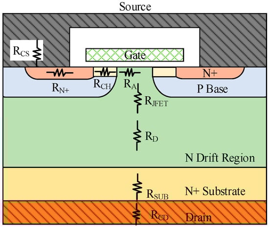
Figure 1.
Components of SiC MOSFET RON.
RCH, RD, and RJFET constitute the primary components of RON [29]. RCH can be simplified and expressed by (2),
µN is composed of four components [30,31], as described in (3). µC dominates low-field mobility under low gate bias at room temperature. In contrast, µSR becomes the predominant factor affecting low-field mobility at higher VG [32].
VTH can be expressed as (4) [10],
The specific JFET resistance is given by (5) [33],
The specific RD is given by (6),
µN_d can be expressed as (7).
RS is defined as the RON excluding RCH [34], and its main components are RJFET and RD.
2.2. Effect of Gate Oxide Degradation on RON
2.2.1. Mechanism of Gate Oxide Degradation
The gate oxide degradation of SiC MOSFETs is one of the most common chip-level degradation modes and can be classified into two types: time-dependent dielectric breakdown (TDDB) and single-event gate rupture (SEGR) [25]. TDDB is the more significant failure mechanism in most applications, which arises mainly from defect accumulation within the gate oxide. TDDB is the more prominent failure mechanism in most applications, primarily caused by the accumulation of defect charges in the oxide layer.
2.2.2. Impact of Gate Oxide Degradation on VTH, µN, and RON
Among the factors contributing to TDDB, both Qit and Qot primarily lead to a reduction in mobility in the SiC MOSFET channel and variations in the threshold voltage. During electron injection into the oxide layer via tunneling, the electrons are captured by near-interface traps (NITs) with energy levels below the conduction band, forming stable negative charges. The accumulation of these negatively charged Qit compensates for the effect of the oxide field. Consequently, a higher electric field is required across the oxide to maintain the channel, which leads to an increase in VTH.
The empirical expression modeling the effect of the gate oxide degradation mechanism on VTH shift is given by (8) [35], where the specific shift in VTH can be defined as ΔVTH_drift.
Meanwhile, the accumulation of both Qot and Qit significantly impacts channel carrier mobility, resulting in a direct reduction in µN [36]. The primary mechanism through which Qit affects this reduction is charge scattering, which directly contributes to mobility degradation [35]. The empirical expression modeling the effect of the gate oxide degradation mechanism on channel mobility is given by (9) [37], which is based on the Single Transistor Mobility Technique.
It can be observed that as the gate degrades, the accumulation of Qit increases, exacerbating this effect and further reducing µN. Therefore, gate oxide degradation not only affects VTH but also deteriorates electron mobility.
COX is the capacitance of the gate oxide layer, determined by the physical dimensions of the gate oxide layer and the permittivity of SiO2 [36]. It remains unaffected by gate degradation and Tj variations. LCH and WCELL are the physical structural dimensions of the SiC MOSFET, which remain constant after chip fabrication and remain unaffected by temperature variations and gate degradation.
As the gate oxide layer of SiC MOSFETs degrades, µN exhibits a significant decline, while VTH shows a clear increase. Meanwhile, COX, LCH, and WCELL remain unaffected during this process. Based on (2), it can be inferred from the analysis that RCH increases with gate degradation. In contrast, according to (5) and (6), RD and RJFET are unaffected by gate degradation, indicating that RS is not significantly influenced by gate degradation.
Therefore, it can be inferred that changes in the RCH component of RON in SiC MOSFETs can serve as a reliable indicator for assessing gate degradation.
2.3. Effect of Temperature on RON
2.3.1. Effect of Temperature on VTH, µN, and RON
The temperature characteristic of VTH can be analyzed based on (4), which shows that it decreases as the temperature increases, as already analyzed in [10]. µN is primarily influenced by surface roughness scattering, which increases with temperature (approximately below 170 °C) [32]. COX, LCH, and WCELL remain unchanged with temperature, which are dependent on the physical parameters of SiC MOSFETs structure.
As a result, based on (2), RCH exhibits a negative temperature coefficient and decreases with increasing temperature, as also verified by [38].
2.3.2. Effect of Temperature on RS
In (7), Nd represents the donor doping concentration, which refers to the fixed number of donor atoms introduced during the doping process to supply free electrons. Nd does not vary with temperature, as it is a fixed physical quantity determined by the doping process. According to (7), the mobility μN_d decreases exponentially with increasing temperature, exhibiting a significant negative temperature dependence. Based on (6), RD is inversely proportional to μN_d. Therefore, as temperature increases, the reduction in mobility directly leads to a significant increase in RD with rising Tj.
This analysis indicates that RD exhibits favorable temperature characteristics, which have also been validated in [38,39]. Since RD is the primary component of RS, it makes RS a reliable parameter for predicting junction temperature.
2.4. Derivation of the RON Model
This chapter presents a RON equation that characterizes the effects of gate degradation and Tj on RON, thereby facilitating the use of RON to predict gate degradation and Tj.
2.4.1. Derivation of the Expression for μN
μN is influenced by VG and temperature [32], which can be described by the empirical Equation (10) [30]. μN is also influenced by gated oxide degradation, as previously explained in (8) and (9).
According to [10,22], when the gate is subjected to positive stress, VTH exhibits a positive shift. This is because, after a certain period of gate degradation, interface traps become dominant. These traps interact with charge carriers and capture electrons, resulting in the formation of negative charges in n-channel MOSFETs, which has been introduced in Section II. Due to Qit dominating in the VTH shift instead of Qot [35], (8) can be simplified to (11),
Meanwhile, based on the approach described in [37], αit >> αot and Qit dominates [36], after which (5) can be simplified to
By substituting (11) into (12) and replacing the unknown variable αit, COX, and q with a new parameter, kun_aged, (13) can be obtained.
Based on (13), the impact of gate degradation on µN can be calculated based on VTH drift. This approach enables ΔVTH_drift to simultaneously characterize the changes in both µN and VTH during gate degradation. The key advantage of this method is that it allows the monitoring of two critical parameters using a single variable, ΔVTH, simplifying the evaluation process and reducing the reliance on additional measurement techniques.
In summary, the expression incorporating the effects of gate degradation, Tj, and VG on µN is derived and presented in (14).
At high gate voltages, surface roughness scattering consistently dominates the behavior of carrier mobility (uN0) across a wide temperature range, and its value remains nearly independent of temperature [32]. In addition, the extracted mobility values from the tested devices in this study also demonstrate a weak dependence of uN0 on temperature. To facilitate the subsequent model formulation and parameter extraction while maintaining high modeling accuracy in high-temperature operating regimes, uN0 is treated as a temperature-independent constant in this work.
2.4.2. Derivation of the Expression for RON
The IDS have a relationship with VG, VTH, VCH, and other parameters as proposed in (15) [29].
By substituting (14) into (15) and accounting for the short-channel effect λ [40], while replacing the temperature- and gate degradation-independent terms COX, LCH, and WCELL, as well as uN0, with a parameter k, the final RON model, as given in (16), can be obtained.
3. Proposed Evaluation Strategy for Gate Degradation and Tj
This section consists of two parts. The first part introduces the parameter calculation method for the RON model, while the second part presents the gate degradation prediction and Tj prediction methods based on the RON model.
3.1. Parameter Calculation of RON Model
The parameters of the RON model can be calculated based on the process, which is illustrated in Figure 2. Both test data before and after gate degradation (110 h HTGB) are used, with the latter applied to calculate kun_aged, and the details are as below:
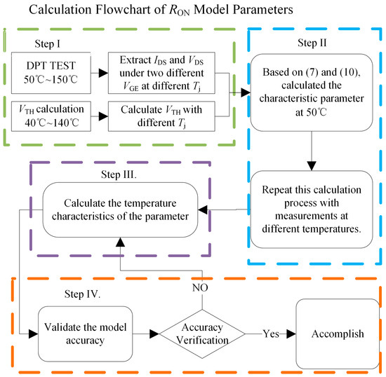
Figure 2.
Parameter calculation process.
- Step 1: DPT and Measurement Aggregation
DPT needs to be conducted under different temperatures, IDS, and two different VG, with the specific testing conditions detailed in Section 4. The measurement is aggregated based on the level of gate oxide degradation, temperature, IDS, and VG.
- 2.
- Step 2~3: Parameter Classification and Initialization
A parameter calculation method based on nonlinear least-squares optimization is proposed. It combines global variables and local variables. The global variables (k, θ, and kun_aged) are the parameters that are not affected by temperature based on the analysis in Section 2, while the local variables (λ and RS) are temperature-dependent. This means that, at the same level of gate degradation, under varying temperatures, gate voltages, and currents, the global variables remain constant, while the local variables change with temperature. The variation characteristics of the local variables are consistent with the physical properties of the parameters analyzed in Section 2.
The ΔVTH is the parameter to indicate the gate oxide degradation that is used to calculate the parameter kun-age. Initial values for these parameters are needed and constrained within predefined bounds to ensure the physical significance and convergence of the algorithm.
- 3.
- Step 4: Model Accuracy Validation
Due to the nonlinearity of RON model, it is difficult to solve directly through the equation. Therefore, an error function is designed to quantify the deviation between the calculated values and experimental data. A computational program based on MATLAB’s nonlinear least-squares solver is developed, which adjusts both global and local parameters to minimize the error. Through iterative calculations, the solution for the conduction impedance model parameters is obtained by minimizing the total error between the calculated and measured RON. The residuals provide a quantitative measure of the model’s fit to the experimental data, validating its overall performance.
Finally, the temperature-independent parameters k, θ, and kun_aged are calculated. Simultaneously, the values of variables (VTH, λ, and RS) at different temperatures are determined, and their temperature functions are established and named fVTH, fλ, and fRS, respectively. The RON model is then constructed according to (16).
3.2. Prediction Method for Junction Temperature and Gate Degradation
The flowchart for estimating the gate degradation and Tj is shown in Figure 3. Based on the RON model, if Tj is known, VTH becomes the only unknown parameter, which can be calculated directly and used to accurately assess the gate degradation level. Similarly, if the gate degradation level (ΔVTH_drift) is known, the Tj can also be accurately calculated because the parameters VTH, λ, and RS can be expressed as functions of Tj, which has been calculated. However, in industrial applications, both the Tj and gate degradation levels are unknown.
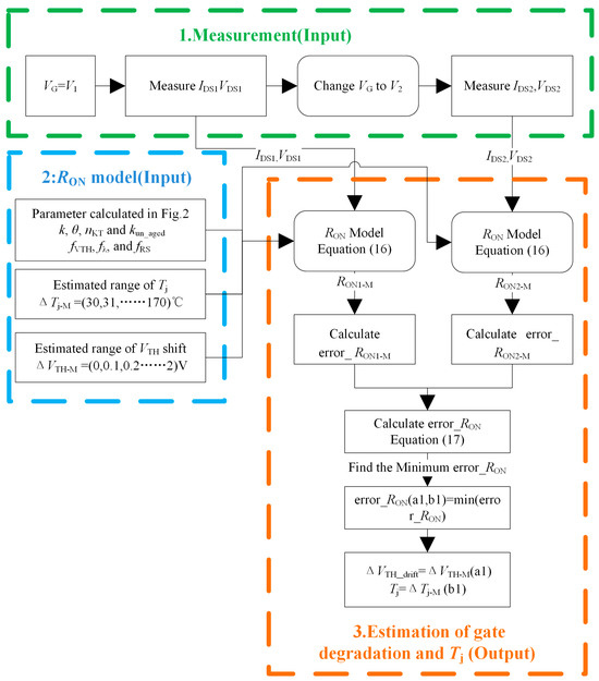
Figure 3.
Gate degradation and Tj calculation process.
To solve this, two sets of IDS and VDS with two different VGS at the same temperature are required, denoted as IDS1, VDS1, IDS2, and VDS2. By substituting these two sets of data into (16), two nonlinear equations are obtained, from which the two unknowns, Tj and ΔVTH_drift, can be simultaneously solved. Solving these nonlinear equations typically requires significant computational resources. To address this, a trial-and-error method is employed in this study. The process is as follows:
First, the ΔVTH_drift matrix (ΔVTH-M) is defined to represent the VTH offset calculation range, while the Tj matrix (Tj_M) represents the temperature range for Tj calculation. Both matrices are one-dimensional, with values incremented by their respective step sizes, and their lengths denoted as n1 and n2, respectively. The range of ΔVTH-M is set from 0 V to 2 V, with a step size of 0.1 V, and the range of Tj_M is from 30 °C to 170 °C, with a step size of 0.01 °C.
Next, under the condition of VGS = V1, the matrix of RON named (RON1_M) is calculated by substituting the measured IDS1 and IDS2 into the RON model, along with the assumed ΔVTH-M and Tj_M. In each iteration, the rows represent variations in ΔVTH-M, while the columns represent variations in Tj_M. This method results in a matrix representing the calculated RON values for the given ΔVTH-M and Tj_M.
Third, the difference between RON1_M and the actual measured RON1 is calculated and recorded as error_RON1_M (17). Similarly, under the condition of VG = V2, the measured IDS2 and VDS2 are substituted into RON model, and the same method is applied to calculate the error between calculation and measurement, named error_RON2_M.
Fourth, the total error (error_RON) is computed based on (17), and the corresponding matrix indices a1 and b1 are identified where the error is minimized. The minimum error_RON occurs when the calculated values of RON1 and RON2, derived from ΔVTH-M (a1) and Tj_M (b1) under the conditions of VGS1 and VGS2, exhibit the least deviation from the measured values. Therefore, ΔVTH-M (a1) and Tj_M (b1) are taken as the estimated values for ΔVTH_drift and Tj, respectively.
Figure 4 illustrates the process of applying the previously described calculation method in actual computations. By inputting VG1, IDS1, VDS1, VG2, IDS2, and VDS2, along with the known RON model, the variation in error_RON is calculated under different assumptions of Tj and ΔVTH. The minimum RON occurs when Tj = 100 °C and ΔVTH = 0.4 V, where the RON1 and RON2 calculated using the RON model exhibit the smallest deviation from the actual measured values. This minimum value of error_RON indicates that, at this point, the calculated RON at the two gate voltages exhibits the smallest error compared to the actual test values. For clarity, the calculations shown in the figure are based on a VTH step size of 0.2 V, with an actual calculation step size of 0.01 V.
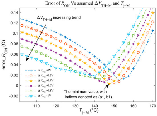
Figure 4.
Computation of error_RON under varying assumptions of Tj-M and ΔVTH-M.
4. Experimental Methodology
4.1. Design of Gate Drive Circuit
To obtain two sets of IDS and VDS with two different VG at the same temperature, a two-level, turn-on gate drive circuit is designed, capable of completing the VG transition within 1 µs. During this transition, the Tj of the SiC MOSFET is assumed to remain constant. Therefore, two sets of IDS and VDS values before and after the gate voltage transition can be measured. It mainly consists of three modules, the control module, the gate drive module, and the VDS detection module, as illustrated in Figure 5 [41].
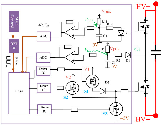
Figure 5.
Illustration of gate drive circuit.
In the gate drive module, S1 and S2 are controlled by the FPGA to achieve efficient and rapid voltage switching, enabling precise control of the turn-on and turn-off states of the SiC MOSFET.
For the VDS detection module, a silicon-based, high-voltage fast recovery diode STTH112 is used to block the DC voltage. This diode is silicon-based and, therefore, does not experience gate degradation. The impact of temperature variations on the forward voltage drop (VF) of D1 is mitigated using a compensation technique with a diode of the same type (D11). Both D1 and D11 are exposed to identical thermal conditions and have similar current conditions, ensuring that the forward voltages of D1 and D11 are similar. In this circuit, R1, R11, R2, and R12 have the same values, allowing AD_VDS to be calculated as (18) [41]:
To reduce noise in the sampling circuit, a FIR filter is applied in the calculation of VDS, effectively mitigating high-frequency noise interference. The actual switching curve of VG is shown in Figure 6. It shows that the switching of VG is completed within 1 μs and the VDS-AD has a significant drop at the same time, which is also stabilized in 1 μs. The reason for the VDS-AD dropping is that RCH decreases as VG increases, which has already been analyzed in (8). This measurement process is performed within one PWM period by the gate drive circuit, without affecting the actual control signals. Additionally, this action has minimal impact on the conduction losses of the SiC MOSFET due to its short duration, lasting only a few microseconds when gate degradation level and Tj estimation are required, with negligible increases in conduction loss (since both V1 and V2 are higher than VTH). This approach can be integrated into the drive circuit, requiring no specific timing or additional control strategies, which has great significance for practical applications.
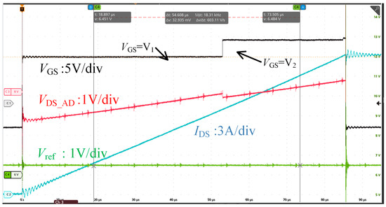
Figure 6.
Actual waveforms of IDS, VGS, and VDS in the DPT Test.
4.2. Experimental Configuration for RON Model Extraction Based on DPT Measurement
A half-bridge inverter based on SiC MOSFETs has been constructed, including a high-voltage power supply, heating equipment, inductive load, power board, and gate driver board, as shown in Figure 7. The current probe N2779A, voltage probe N2790A, and oscilloscope (Agilent MSO44) are used to capture the IDS, VREF, and VDS-AD. An electric heating plate (BK946S) is used to heat the DUT to the set temperature, and a thermocouple is attached to the DUT for temperature verification. The configuration of the experimental equipment and the test conditions are shown in Table 1.
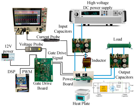
Figure 7.
Experimental setup for the DC-DC (boost) converter.

Table 1.
Test information for the RON model.
4.3. Experimental Configuration for Validation of the Proposed Method in the DC-DC Converter
To verify the effectiveness of the proposed strategy, this paper designed an experimental method based on a DC-DC converter to evaluate Tj and gate degradation. A SiC MOSFET from ROHM, model SCT3080KR, was selected, featuring a typical voltage rating of 1200 V, a typical RDS of 80 mΩ at 25 °C, and IDS of 22 A at 100 °C. The experimental setup is also illustrated in Figure 7, and the topology of the converter is a boost circuit. The control circuit utilized a DSP (model: TMS320F28335) to generate control signals by monitoring input and output voltages. The input bus voltage was fixed at 100 V, with the duty cycle ranging from 0.5 to 0.7, and the output voltage was adjusted according to the duty cycle. To accommodate the DUT’s current-carrying capability, the duty cycle was adjusted to regulate the inductor current, resulting in a current range of 10.5 A to 18 A flowing through the SiC MOSFET before and after the gate transition. Additionally, the experimental temperature range was set to 50~150 °C. The details are listed in Table 2.
Table 2.
Key information of invertor test for DUT1.
4.4. Experimental Configuration for Accelerated Testing of Gate Oxide Degradation
To evaluate the impact of gate oxide degradation on device performance and reliability, this paper adopts the High-Temperature Gate Bias (HTGB) test as the accelerated degradation method. Following the JEDEC standard (JESD22-A108D) [42], the HTGB test applies high electric field stress under elevated temperatures to simulate the operational stress experienced by devices during prolonged usage, thereby accelerating the degradation of the gate oxide [25]. In this experiment, the test conditions were set to a VGS of 30 V and a temperature of 175 °C. These conditions ensure that the experimental results accurately reflect the actual influence of gate degradation on device performance, providing reliable data for further analysis.
To simulate long-term operational degradation, the DUT underwent five HTGB aging tests. After each aging test, a VTH extraction test was conducted to measure and analyze the changes in VTH of the DUT at different stages of degradation. After the first and third aging tests, DPT experiments were performed to measure and analyze the variations in RON at different degradation stages, which were also used to establish the RON model. After the fifth aging test, the DUT was installed in a DC-DC inverter for continuous pulse testing to validate the effectiveness and reliability of the proposed method.
5. Experimental Verification
This section includes five experimental results: (1) the extraction of VTH under different accelerated aging times, (2) the results of the double-pulse test, (3) the extraction of on-resistance based on the double-pulse test, (4) the prediction of junction temperature aging and gate degradation aging based on the double-pulse test, and (5) the prediction results of junction temperature and gate aging based on the DC-DC converter.
5.1. Experimental Results of VTH Extraction and Gate Oxide Degradation
Figure 8 illustrates the variations in the VTH under different temperatures and degradation levels, with the calculations based on the transfer characteristics curve measured by B1505. It can be observed that, regardless of whether the device is degraded or not, VTH consistently decreases with increasing temperature. Furthermore, under gate degradation conditions, the magnitude of VTH shift increases significantly as the level of degradation intensifies, which aligns with the theoretical analysis presented in (8).
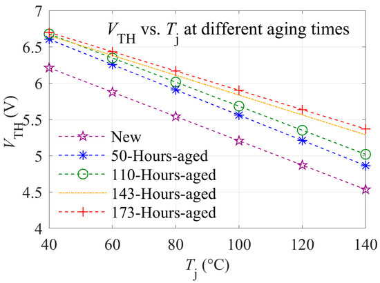
Figure 8.
VTH extraction results of DUT at different aging times.
5.2. Experimental Results of DPT Test
Figure 9 illustrates the RON of the DUT before and after the aging test, which was obtained through DPT under varying VG, IDS, and Tj conditions. The results show that RON increases with rising Tj, while it significantly decreases as VG increases. This demonstrates the contrasting influence of Tj and VG on the RON of the device.
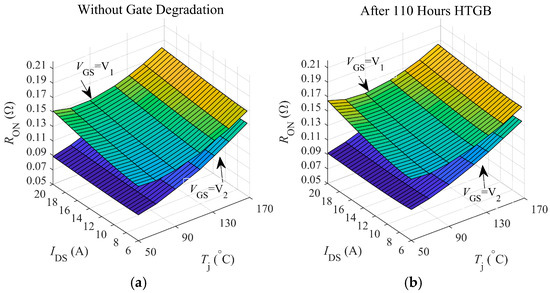
Figure 9.
RON test results under non-aging and aging conditions: (a) non-aging, (b) aged for 110 h.
5.3. Experimental Results of RON Model Calculation
The RON model of the DUT1 was calculated based on the method described in Section 3 and the experimental data obtained in the previous section. The calculated results for the key parameters of the RON model are listed in (19).
To validate the accuracy of the model, the calculated RON with the model was compared with the experimentally measured values. The results for new and 110 h-aged were in Figure 10a and 10b, respectively. The comparison error is defined as kerror and its calculation method is shown in (20).
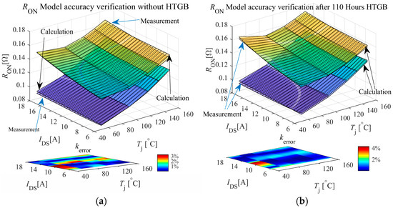
Figure 10.
Comparison of RON model-calculated result and DPT measurement. (a) Without HTGB test. (b) After 110 h HTGB test of DUT1.
5.3.1. Without Gate Oxide Degradation Conditions
In the IDS range of 5 A to 18 A and Tj range of 50 °C to 160 °C, the relative error between calculation and measurement remained within 3%, as shown in Figure 10a. This indicates that the model demonstrates high accuracy and reliability under non-degraded conditions.
5.3.2. Under Gate Oxide Degradation Conditions
When gate degradation occurs at 110 h, the RON values calculated using the same model were compared with the measured values shown in Figure 10b. The results indicate that even under gate degradation, the calculated RON values maintain accuracy within a 4% error margin. The proposed conduction impedance model exhibits excellent accuracy under both non-degraded and gate-degraded conditions, with the error consistently controlled within 4%.
5.4. Prediction Results of Gate Oxide Degradation and Tj Based on DPT
5.4.1. The Explanation of the Calculation Process for Gate Degradation and Tj
Based on the known relationship between the parameters of the RON model and temperature, ΔVTH_drift and Tj are solved to minimize the error between the RON model results and the actual test data (minimize error_RON). The corresponding values of ΔVTH_drift and Tj at the minimum error represent the final solution. Taking the prediction of ΔVTH_drift and Tj after 110 h of HTGB at 146 °C as an example, Figure 11 shows the variations in error_RON (the sum of the absolute errors between the calculated RON1 and RON2) under different ΔVTH and Tj assumptions. It can be observed that when ΔVTH_drift is 0.4 V and Tj is 148.1 °C, the error_RON reaches its minimum value. The predicted results at this point closely match the actual Tj of 146 °C and VTH deviation of 0.5 V (Figure 8), validating the effectiveness of this method for predicting gate degradation and junction temperature.
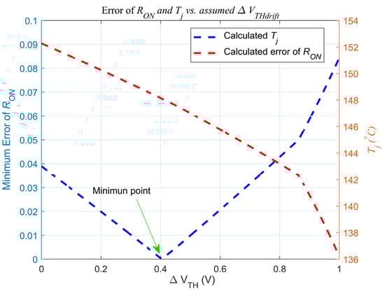
Figure 11.
Variations in error_RON under different ΔVTH drift and Tj assumptions for predicting gate degradation and junction temperature after 110 h of HTGB at 146 °C.
5.4.2. Experimental Conditions and Results
The gate degradation and Tj of the device are predicted under different temperatures, gate degradation levels, and current conditions based on DPT. For both before aging and after 110 h of aging, the gate degradation and Tj of DUT1 were predicted at six temperatures between 70 °C and 168 °C. At each temperature, six current levels were selected. The prediction results are presented in Figure 12 and Figure 13.
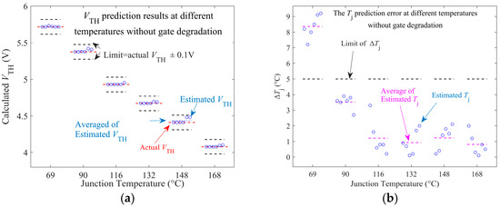
Figure 12.
Tj and VTH estimates of unaged DUT1. (a) VTH. (b) Tj.
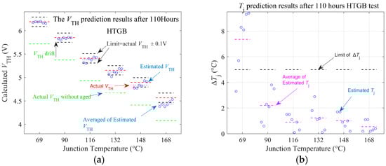
Figure 13.
Tj and VTH estimated after 110 h HTGB of DUT1. (a) VTH. (b) Tj.
The prediction results for gate degradation and Tj within the temperature range of 69 °C to 170 °C for the non-aged DUT are presented in Figure 12. Specifically, Figure 12a illustrates the estimation results of Tj, while Figure 12b shows the results for VTH. The results indicate that, for the non-aged DUT, the accuracy of the VTH is less than 0.1 V from 70 °C to 170 °C; this is because the effect of gate degradation on RON is characterized to possess VTH. At the same time, the maximum absolute error of the estimation remains below 5 °C when Tj is in the range of 90~150 °C. Moreover, as Tj increases, the accuracy improves significantly, achieving an error range of 2~3 °C at 110 °C~168 °C. The observed improvement is primarily due to the temperature-dependent behavior of the RD, which plays a dominant role at elevated temperatures, as indicated by (7). The estimated error of Tj at 69 °C is near 9 °C, primarily due to the 3% accuracy of the RON model in this temperature range and the relatively small contribution of RS at lower temperatures based on Figure 10.
Figure 13a presents the Tj and VTH prediction results after 110 h of HTGB. After 110 h of aging, VTH exhibits a significant shift from its original value (marked in green) to the aged value (marked in red). The degree of this shift varies at different temperatures, indicated by the purple markings. However, the proposed method calculates VTH with an error of less than 0.2 V compared to the VTH measurement, within the temperature range of 69 °C to 169 °C under these aging conditions. This is because the RON model uses kun_aged, which expresses the impact of gate degradation on µN through VTH. Therefore, the RON model can characterize the impact of gate degradation on RON solely through VTH. The Tj prediction achieves an error of less than 5 °C across the temperature range of 50 °C to 150 °C, maintaining the same level of accuracy as with under unaged conditions. These results validate that the proposed method can simultaneously achieve accurate Tj prediction and gate degradation verification under DPT, across different samples and aging conditions.
5.5. Experimental Results Based on a DC-DC Converter
To validate the accuracy of the method proposed in this paper at the inverter level, DC-DC (boost) inverter-based predictions of gate degradation and Tj were conducted for the test sample under 173 h of gate degradation conditions. The details of the DC-DC inverter have been described in Section 4. The DUT was heated by the hot plate as the initial temperature. Under the same temperature conditions, during the first 20 ms of continuous operation, 10 pulses with varying currents are selected for Tj prediction. The 20 ms duration is chosen because, due to the thermal resistance and capacitance of the MOSFET, the junction temperature of the device remains relatively stable during this period.
Figure 14 displays the waveforms of VG, VDS, and IDS at 145 °C. It can be observed that VGS increases rapidly while RON decreases simultaneously, consistent with the results of the DPT test. Since the FPGA manages the VG transition command in the gate driver circuit, it can easily perform IDS1 and VDS1 sampling before the transition and then capture IDS2 and VDS2 1 µs after the VGS transition. To reduce sampling errors throughout the testing process, three points are selected before and after the transition, and their average values are used for calculating named IDS and VDS. This testing and calculation process were repeated under different temperature conditions to ensure the reliability and consistency of the data, with the results shown in Figure 15. Both the VTH and Tj can be calculated based on (16) and Figure 3, which is the same as the DPT test.
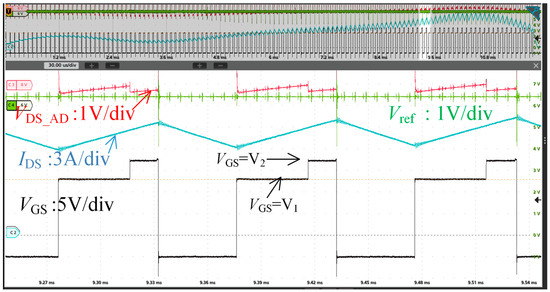
Figure 14.
Actual waveforms of VDS, VGS, and IDS of DUT1 in the DC-DC Converter.
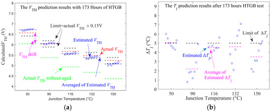
Figure 15.
Tj and VTH estimated after 173 h HTGB test (a) VTH. (b) Tj.
Figure 15a,b present the estimated VTH and Tj results after 173 h of accelerated gate degradation testing in the DC-DC inverter. It is observed that the maximum error of VTH is below 0.2 V between 50 and 150 °C, which is slightly higher than that of the unaged and 110 h-aged conditions. This indicates that, although the calculation of kun_aged relies only on data from the unaged and 110 h aging stages, the error in the VTH calculation at the 173 h aging stage increases by only 0.05 V while still maintaining good accuracy.
5.6. Impact of Voltage and Current on the Proposed Method
The RON is insensitive to the DC voltage, which has been verified by [41]. According to (2) and (6), RON is sensitive to current variations; however, the RON model has effectively characterized the relationship between current and RON, which ensures that variations in current do not significantly affect the prediction accuracy. In the validation of both the DPT and DC-DC inverter tests, a different current was used. The current values in the DC-DC tests are shown in Figure 16, with each point corresponding to the current value of the respective point in Figure 15. The blue color represents the average of three sampling points at VG = V1, while the red color represents the average of three sampling points at VG = V2. The results show that changes in current do not significantly impact the prediction accuracy. This is because the RON model effectively decouples the relationship between current and RON, thus maintaining the prediction accuracy.
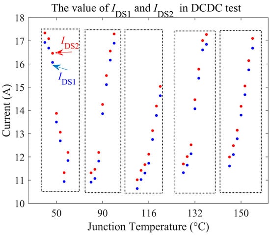
Figure 16.
Average value of IDS1 and IDS2 (before and after VG changing) in the DC-DC test.
5.7. Gate Oxide Degradation and Tj Prediction Results Based on Planar SiC MOSFET
To validate the effectiveness of this method on planar SiC MOSFETs, DUT 2 was selected for DPT testing. The DPT test method, gate drive circuit, and parameter extraction process are consistent with DUT1. The current of the tested sample has been adjusted according to the rated current of DUT2, and the specific test data is shown in Table 3.
Table 3.
Test information for the RON model of DUT2.
The calculated results for the key parameters of the RON model for DUT2 are presented in (21).
The RON calculated by the model were compared with the experimentally measured results, with the results for the new sample presented in Figure 17. The error is defined as kerror as provided in (20). As shown within the measurement range in Table 3, the accuracy of the RON model is within 5%, which is consistent with the results shown in Figure 10. This demonstrates that the RON model extracted using this method maintains accuracy for the unaged condition and is also applicable to planar SiC MOSFET.
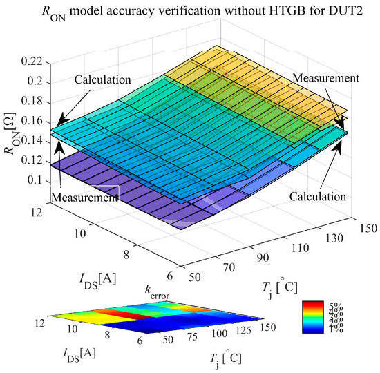
Figure 17.
Comparison of the RON model with DPT measurement for DUT2 without gate degradation.
For three different gate degradation levels (new, after 70 h of HTGB, and after 96 h of HTGB), the gate degradation and Tj of DUT2 were predicted using the method proposed in this paper at five different temperatures within the range of 70 °C to 148 °C. At each temperature, six different currents were selected for measurement, with the current range provided in Table 3. The corresponding prediction results are shown in Figure 18.
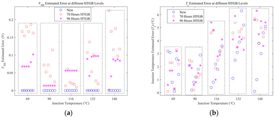
Figure 18.
Tj and VTH estimated result with unaged, after 70 h HTGB, after 96 h HTGB of DUT2 test. The current range is from 6 A to 12 A. (a) VTH. (b) Tj.
It can be observed that as DUT2 is unaged, the prediction of VTH within the range of 70 °C to 148 °C demonstrates high accuracy. This is attributed to the fact that the RON model was primarily calibrated based on the unaged condition. Additionally, it can be observed that the prediction error of the Tj is within 6 °C, which is due to a certain difference between the RON model and the actual test data. After 70 h and 96 h of aging, the prediction error of VTH is within 0.2 V, except for one point. Although it is slightly larger compared to DUT1, it still accurately characterizes the gate degradation. At this stage, the prediction accuracy of Tj is also within 6 °C, similar to the results of DUT1. Therefore, the above tests demonstrate the effectiveness of the proposed method in different SiC MOSFET structures under varying degrees of gate degradation and junction temperature.
5.8. Comparison of Porposed Method with Conventional RON Mapping Methods Without Considering Gate Degradation
Based on the experimental data obtained from unaged devices at a gate voltage of VG equals 16.2 V, a mapping relationship among RON, junction temperature Tj, and current was established. The conventional one-dimensional look-up table method [22], which does not account for gate degradation effects, was then used to predict junction temperature under the conditions shown in Figure 15b. The prediction results were compared with those obtained by the proposed method, as shown in Figure 19.
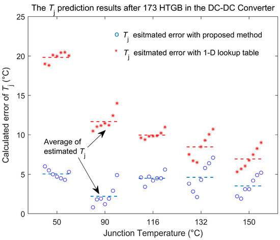
Figure 19.
Comparison of the proposed model to the conventional RON mapping models for DUT1 after 173 h HTGB.
It is clearly observed that the conventional one-dimensional look-up table method exhibits significantly increased errors after gate degradation. For example, the prediction error at 69 °C reaches 20 °C, which is about 15 °C higher than that of the proposed method. At 160 °C, the average prediction error for the conventional method is 6.9 °C, while the proposed method reduces it to 3.5 °C.
The main reason for the significant decline in accuracy of the conventional method is that it does not consider the effects of gate degradation, specifically the positive shift in threshold voltage and the reduction in carrier mobility, both of which lead to increased channel resistance. At lower temperatures, channel resistance represents a larger proportion of the total RON, making RON more sensitive to gate degradation effects. Ignoring these effects can easily result in large prediction errors.
In contrast, the proposed RON model inherently accounts for these degradation factors, not only significantly improving the accuracy of junction temperature prediction compared to the conventional method, but also enabling quantitative evaluation of gate oxide degradation, thereby improving the accuracy and practical utility of device health assessment.
5.9. The Limitations of the Proposed Method
Package degradation can also alter the relationship between RON and temperature. In power second cycling tests of power devices, package degradation increases the contact resistance at the bond wires and die surface, while in minute-level power cycling, it increases the contact resistance at the interface between the chip and substrate. When package degradation occurs, the increase in contact resistance alters the relationship between RS and temperature, potentially affecting the accuracy of the proposed method. The primary cause of package degradation is related to the packaging process, and its impact can be mitigated through advancements in packaging technologies. For example, the widespread application of silver sintering [43] and direct copper bonding (DTS) technologies in high-reliability applications, such as electric vehicles, has significantly reduced the impact of package degradation on device performance.
Gate degradation is caused by the design of the gate oxide layer in SiC MOSFETs, which requires improvements in the chip design. The method proposed in this paper primarily focuses on the analysis and prediction of gate degradation and does not address package degradation.
To focus on accuracy at a high-temperature range (50–175 °C), this work assumes uN0 to be temperature-independent. However, this may introduce deviations at lower temperatures due to the increasing role of temperature-dependent scattering mechanisms.
6. Conclusions
This paper primarily investigates the use of the RON model for gate oxide degradation and Tj prediction in SiC MOSFETs, addressing the challenge that existing evaluation methods focus on a single aspect and fail to integrate both targets effectively. During operation, variations in RON, driven by gate voltage changes, are strongly correlated with both Tj and gate degradation. By extracting the temperature dependencies of the parameters in the RON model, all parameters are expressed as functions of temperature, leaving Tj and ΔVTH_drift as the only unknowns. By using two sets of IDS and VDS measurements, taken before and after the gate voltage change, both Tj and ΔVTH_drift can be derived from the RON model. Experimental results under DPT test conditions, the VTH prediction error for DUT1 remains within 0.2 V across the temperature range of 70 °C to 140 °C, both before and after 110 h of HTGB. The Tj prediction error is within 6 °C when Tj is above 96 °C. For DUT2, the prediction error of VTH remains within 0.2 V in the temperature range of 69 °C to 148 °C, under no aging, 70 h of HTGB, and 96 h of HTGB, with Tj prediction accuracy within 6 °C. DUT1 was tested under DC-DC boost inverter conditions after 173 h of HTGB using the proposed method. The VTH prediction accuracy remained within 0.2 V across the temperature range of 50 °C to 150 °C, consistent with the results obtained under DPT test conditions. These results validate that the proposed method effectively estimates both Tj and gate degradation levels in SiC MOSFETs.
This paper integrates the RON model with the gate driver circuit to simultaneously estimate both Tj and VTH, offering a novel approach for SiC MOSFET reliability assessment. Future work will focus on improving the accuracy of both Tj and VTH.
Author Contributions
Conceptualization, P.W. and Z.Z.; methodology, P.W.; software, P.W.; validation, P.W.; investigation, Z.Z.; resources, Z.Z.; writing—original draft preparation, P.W.; writing—review and editing, P.W.; visualization, Z.Z.; supervision, Z.Z. All authors have read and agreed to the published version of the manuscript.
Funding
This research received no external funding.
Data Availability Statement
All experimental data used in this study were measured using laboratory equipment and are available in CSV format. The datasets are available from the corresponding author upon reasonable request.
Conflicts of Interest
The authors declare no conflict of interest.
Nomenclature
| Ad | Device active area |
| COX | Gate oxide capacitance |
| kB | Boltzmann constant |
| LCH | Length of channel |
| Ld | Equivalent length |
| ni | Intrinsic carrier concentration |
| NA | Doping concentration in the p-type well |
| Nd | Doping concentration in the drift region |
| ΔNit | Variation in interface trap densities |
| Nit | Stress-induced changes in densities of Qit |
| Not | Stress-induced changes in densities of Qot |
| q | Electric charge |
| Qit | Interface-trapped charge at the oxide–silicon interface |
| Qot | Oxide-trapped charge within the gate oxide |
| RA | Resistance of accumulation |
| RCH | Resistance of channel zone |
| RCS | Resistance of source contact |
| RCD | Resistance of drain contact |
| RD | Resistance of drift zone |
| RJFET | Resistance of JFET zone |
| RN+ | Resistance of the source region |
| RON | Resistance of on-state |
| RS | Residual resistance |
| RSUB | Resistance of the N+ substrate |
| T0 | Reference temperature |
| Tj | Temperature of junction temperature |
| VG | Gate-source voltage |
| VTH | Threshold voltage |
| ΔVTH_drift | Drift of VTH due to gate degradation |
| WCELL | Width of channel zone |
| α | Effective width for vertical current flow through the JFET region |
| αit | Fitting coefficients in the model for describing the effects of Qit |
| αot | Fitting coefficients in the model for describing the mobility reduction of interface-trapped charges induced by Qot |
| ρJFET | Resistivity of the JFET region |
| θ | Electric Field Reduction Parameter |
| λ | Coefficient of short-channel effect |
| µN | Electron mobility of the semiconductor interface of the oxide layer |
| µN_d | Drift region mobility |
| µN0 | Intrinsic electron mobility of the inversion layer |
| µB | Semiconductor material’s electron mobility |
| µPH | Surface phonon mobility |
| µC | Coulombic scattering |
| µSR | Surface roughness mobility |
| εS | Dielectric constant |
| χjp | Depth of the P+ shield region |
References
- Jiang, X.; Wang, J.; Yu, H.; Chen, J.; Zeng, Z.; Yang, X.; Shen, Z.J. Online junction temperature measurement for SiC MOSFET based on dynamic threshold voltage extraction. IEEE Trans. Power Electron. 2021, 36, 3757–3768. [Google Scholar] [CrossRef]
- Yang, S.; Bryant, A.; Mawby, P.; Xiang, D.; Ran, L.; Tavner, P. An Industry-Based Survey of Reliability in Power Electronic Converters. IEEE Trans. Ind. 2011, 47, 1441–1451. [Google Scholar] [CrossRef]
- Lelis, A.J.; Green, R.; Habersat, D.B.; El, M. Basic Mechanisms of Threshold-Voltage Instability and Implications for Reliability Testing of SiC MOSFETs. IEEE Trans. Electron. Devices 2015, 62, 316–323. [Google Scholar] [CrossRef]
- Farhadi, M.; Vankayalapati, B.T.; Sajadi, R.; Akin, B. Gate-Oxide Degradation Monitoring of SiC MOSFETs Based on Transfer Characteristic with Temperature Compensation. IEEE Trans. Transp. Electrif. 2024, 10, 1837–1849. [Google Scholar] [CrossRef]
- Afanasev, V.; Bassler, M.; Pensl, G.; Schulz, M. Intrinsic SiC/SiO2 interface states. Phys. Status Solidi 1997, 162, 321–337. [Google Scholar] [CrossRef]
- Karki, U.; Peng, F.Z. Precursors of Gate-Oxide Degradation in Silicon Carbide MOSFETs. In Proceedings of the 2018 IEEE Energy Conversion Congress and Exposition (ECCE), Portland, OR, USA, 23–27 September 2018. [Google Scholar]
- Kang, J.; Liu, Q.; Luo, H.; Cao, H.; Zhang, Z.-H.; Xin, Z. Investigation of off-state stress induced degradation of SiC MOSFETs under short-circuit condition. IEEE Trans. Ind. Electron. 2023, 70, 5224–5234. [Google Scholar] [CrossRef]
- Zhang, Q.; Zhang, P. A Novel Model of the Aging Effect on the ON-State Resistance of SiC Power MOSFETs for High-Accuracy Package-Related Aging Evaluation. IEEE Trans. Ind. Electron. 2023, 70, 9495–9504. [Google Scholar] [CrossRef]
- Zhang, Q.; Zhang, P. A Junction Temperature and Package Aging Decoupling Evaluating Method for SiC MOSFETs Based on the Turn-on Drain-Source Current Overshoot. IEEE Trans. Power Electron. 2023, 38, 14537–14546. [Google Scholar] [CrossRef]
- Yang, F.; Ugur, E.; Akin, B. Evaluation of aging’s effect on temperature-sensitive electrical parameters in SiC mosfets. IEEE Trans. Power Electron. 2020, 35, 6315–6331. [Google Scholar] [CrossRef]
- Gonzalez, J.O.; Alatise, O.; Hu, J.; Ran, L.; Mawby, P.A. An investigation of temperature-sensitive electrical parameters for SiC Power MOSFETs. IEEE Trans. Power Electron. 2017, 32, 7954–7966. [Google Scholar] [CrossRef]
- Lu, X.; Wang, L.; Yang, Q.; Yang, F.; Gan, Y.; Zhang, H. Investigation and comparison of temperature-sensitive electrical parameters of SiC mosfet at extremely high temperatures. IEEE Trans. Power Electron. 2023, 38, 9660–9672. [Google Scholar] [CrossRef]
- Xue, P.; Davari, P. A Temperature-Dependent Analytical Transient Model of SiC MOSFET in Half-Bridge Circuits. IEEE Trans. Power Electron. 2025, 40, 892–905. [Google Scholar] [CrossRef]
- Niu, H.; Lorenz, R.D. Sensing Power MOSFET junction temperature using gate drive turn-on current transient properties. IEEE Trans. Ind. Appl. 2016, 52, 1677–1687. [Google Scholar] [CrossRef]
- Zhang, Q.; Zhang, P. An online junction temperature monitoring method for SiC MOSFETs based on a novel gate conduction model. IEEE Trans. Power Electron. 2021, 36, 11087–11096. [Google Scholar] [CrossRef]
- Zhang, Z.; Dyer, J.; Wu, X.; Wang, F.; Costinett, D.; Tolbert, L.M.; Blalock, B.J. Online junction temperature monitoring using intelligent gate drive for SiC power devices. IEEE Trans. Power Electron. 2019, 34, 7922–7932. [Google Scholar] [CrossRef]
- Dou, J.; Wang, Z.; Xin, G.; Shi, X. High-Accuracy Online Junction Temperature Measurement of Medium-Voltage SiC MOSFETs Based on Passive Turn-On Delay Time Integrator. IEEE Trans. Power Electron. 2025, 40, 4775–4779. [Google Scholar] [CrossRef]
- Wang, Y.; Jiang, X.; Shi, X.; Liu, Q.; Zhang, S.; Ouyang, R.; Jia, D.; Ma, N.; Gong, X. Online junction temperature estimation for SiC MOSFETs using drain voltage falling edge time. IEEE Trans. Electron. Devices 2023, 70, 5228–5235. [Google Scholar] [CrossRef]
- Du, M.; Liu, F.; Yin, J.; Dong, C.; Ouyang, Z. Junction temperature correction method for SiC MOSFET based on turn-off oscillation frequency of drain-source voltage. IEEE Trans. Electron. Devices 2024, 71, 6208–6215. [Google Scholar] [CrossRef]
- Quan, Y.; Pan, R.; Liu, T.; Zhou, X.; Feng, J.; Tian, Y.; Zheng, L.; Cheng, X. Online Junction Temperature Monitoring Method for SiC MOSFETs Based on Turn-Off Miller Plateau Voltage. IEEE Trans. Power Electron. 2024, 39, 15800–15810. [Google Scholar] [CrossRef]
- Hayashi, S.-I.; Wada, K. Operational Verification of Gate Drive Circuit with Condition Monitoring Function for Gate Oxide Degradation of SiC MOSFETs. IEEE Open J. Power Electron. 2024, 5, 709–717. [Google Scholar] [CrossRef]
- Stella, F.; Pellegrino, G.; Armando, E.; Daprà, D. Online junction temperature estimation of SiC power MOSFETs through on-state voltage mapping. IEEE Trans. Ind. Appl. 2018, 54, 3453–3462. [Google Scholar] [CrossRef]
- Luo, H.; Iannuzzo, F.; Turnaturi, M. Role of Threshold Voltage Shift in Highly Accelerated Power Cycling Tests for SiC MOSFET Modules. IEEE J. Emerg. Sel. Top. Power Electron. 2020, 8, 1657–1667. [Google Scholar] [CrossRef]
- Yang, F.; Pu, S.; Xu, C.; Akin, B. Turn-on delay based real-time junction temperature measurement for SiC MOSFETs with aging compensation. IEEE Trans. Power Electron. 2021, 36, 1280–1294. [Google Scholar] [CrossRef]
- Farhadi, M.; Yang, F.; Pu, S.; Vankayalapati, B.T.; Akin, B. Temperature-independent gate-oxide degradation monitoring of SiC MOSFETs based on junction capacitances. IEEE Trans. Power Electron. 2021, 36, 8308–8324. [Google Scholar] [CrossRef]
- Ye, X.; Chen, C.; Wang, Y.; Zhai, G.; Vachtsevanos, G.J. Online Condition Monitoring of Power MOSFET Gate Oxide Degradation Based on Miller Platform Voltage. IEEE Trans. Power Electron. 2017, 32, 4776–4784. [Google Scholar] [CrossRef]
- Karki, U.; González-Santini, N.S.; Peng, F.Z. Effect of Gate-Oxide Degradation on Electrical Parameters of Silicon Carbide MOSFETs. IEEE Trans. Electron. Devices 2020, 67, 2544–2552. [Google Scholar] [CrossRef]
- Liu, J.; Yao, B.; Wei, X.; Zhang, Y.; Wang, H. An Online Gate Oxide Degradation Monitoring Method for SiC Mosfets Based on Turn-On Gate Voltage Filtering. IEEE Trans. Power Electron. 2024, 39, 5020–5026. [Google Scholar] [CrossRef]
- Lutz, J.; Schlangenotto, H.; Scheuermann, U.; De Doncker, R. Semiconductor Power Devices—Physics, Characteristics, Reliability; Springer: Cham, Switzerland, 2018; pp. 293–295. [Google Scholar]
- Kimoto, T.; Cooper, J.A. Fundamentals of Silicon Carbide Technology: Growth, Characterization, Devices and Applications; John Wiley & Sons: Hoboken, NJ, USA, 2014; pp. 314–319. [Google Scholar]
- Pérez-Tomás, A.; Brosselard, P.; Godignon, P.; Millan, J. Field-effect mobility temperature modeling of 4H-SiC metal-oxide-semiconductor transistors. J. Appl. Phys. 2006, 100, 114508. [Google Scholar] [CrossRef]
- Yang, L.; Bai, Y.; Li, C.; Chen, H.; Han, Z.; Tang, Y.; Hao, J.; Yang, C.; Tian, X.; Lu, J.; et al. Analysis of Mobility for 4H-SiC N/P-Channel MOSFETs Up To 300 °C. IEEE Trans. Electron. Devices 2021, 68, 3936–3941. [Google Scholar] [CrossRef]
- Agarwal, A.; Baliga, B.J. Implant straggle impact on 1.2 kV SiC power MOSFET static and dynamic parameters. IEEE J. Electron. Devices Soc. 2022, 10, 245–255. [Google Scholar] [CrossRef]
- Rumyantsev, S.L.; Shur, M.S.; Levinshtein, M.E.; Ivanov, P.A.; Palmour, J.W.; Agarwal, A.K.; Hull, B.A.; Ryu, S.-H. Channel mobility and on-resistance of vertical double implanted 4H-SiC MOSFETs at elevated temperatures. Semicond. Sci. Technol. 2009, 24, 075011. [Google Scholar] [CrossRef]
- Karki, U.; Peng, F.Z. Effect of Gate-Oxide Degradation on Electrical Parameters of Power MOSFETs. IEEE Trans. Power Electron. 2018, 33, 10764–10773. [Google Scholar] [CrossRef]
- Chaturvedi, M.; Dimitrijev, S.; Haasmann, D.; Moghadam, H.A.; Pande, P.; Jadli, U. Comparison of Commercial Planar and Trench SiC MOSFETs by Electrical Characterization of Performance-Degrading Near-Interface Traps. IEEE Trans. Electron. Devices 2022, 69, 6225–6230. [Google Scholar] [CrossRef]
- Stojadinovic, N.; Manic, I.; Davidovic, V.; Danković, D.; Djorić-Veljković, S.; Golubović, S.; Dimitrijev, S. Electrical stressing effects in commercial power VDMOSFETs. IEE Proc. Circuits Devices Syst. 2006, 153, 281–288. [Google Scholar] [CrossRef]
- Chen, S.; Cai, C.; Wang, T.; Guo, Q.; Sheng, K. Cryogenic and high temperature performance of 4H-SiC power MOSFETs. In Proceedings of the 2013 Twenty-Eighth Annual IEEE Applied Power Electronics Conference and Exposition (APEC), Long Beach, CA, USA, 17–21 March 2013; pp. 207–210. [Google Scholar]
- Zhou, W.; Zhong, X.; Sheng, K. High temperature stability and the performance degradation of SiC MOSFETs. IEEE Trans. Power Electron. 2014, 29, 2329–2337. [Google Scholar] [CrossRef]
- Yin, S.; Tu, P.; Wang, P.; Tseng, K.J.; Qi, C.; Hu, X.; Zagrodnik, M.; Simanjorang, R. An accurate subcircuit model of SiC half-bridge module for switching-loss optimization. IEEE Trans. Ind. Appl. 2017, 53, 3840–3848. [Google Scholar] [CrossRef]
- Zhao, Z.; Wang, P.; Chen, T. A Gate Degradation Independent Online Junction Temperature Estimation Method for SiC MOSFETs Based on Residual Resistance. IEEE Trans. Power Electron. 2024, 39, 13771–13782. [Google Scholar] [CrossRef]
- JESD22-A108D; Temperature, Bias, and Operating Life. JEDEC Solid State Technology Association: Arlington, VA, USA, 2010.
- Yasui, K.; Hayakawa, S.; Funaki, T. Reliability Improvement of 3.3 kV Full-SiC Power Modules for Power Cycling Tests with Sintered Copper Die Attach Technology. IEEE Trans. Compon. Packag. Manuf. Technol. 2023, 13, 1476–1485. [Google Scholar] [CrossRef]
Disclaimer/Publisher’s Note: The statements, opinions and data contained in all publications are solely those of the individual author(s) and contributor(s) and not of MDPI and/or the editor(s). MDPI and/or the editor(s) disclaim responsibility for any injury to people or property resulting from any ideas, methods, instructions or products referred to in the content. |
© 2025 by the authors. Licensee MDPI, Basel, Switzerland. This article is an open access article distributed under the terms and conditions of the Creative Commons Attribution (CC BY) license (https://creativecommons.org/licenses/by/4.0/).