Article

Prediction of the Probability of IC Failure and Validation of Stochastic EM-Fields Coupling into PCB Traces Using a Bespoke RF IC Detector

by
Arunkumar Hunasanahalli Venkateshaiah
1,*,
John F. Dawson
1,
Martin A. Trefzer
1,
Haiyan Xie
2,
Simon J. Bale
1,
Andrew C. Marvin
1 and
Martin P. Robinson
1
1
The School of Physics, Engineering and Technology, University of York, York YO10 5DD, UK
2
Northwest Institute of Nuclear Technology, Xi’an 710025, China
*
Author to whom correspondence should be addressed.
Electronics 2025, 14(11), 2187; https://doi.org/10.3390/electronics14112187
Submission received: 6 April 2025 / Revised: 11 May 2025 / Accepted: 26 May 2025 / Published: 28 May 2025
(This article belongs to the Special Issue Antennas and Microwave/Millimeter-Wave Applications)

Abstract

:
In this paper, a method of estimating the probability of susceptibility of a component on a circuit board to electromagnetic interference (EMI) is presented. The integrated circuit electromagnetic compatibility (IC EMC) standard IEC 62132-4 enables the assessment of the susceptibility of an IC by determining the forward power incident on each pin required to induce a malfunction. Although we focus on IC susceptibility, the method might be applied to other components and sub-circuits where the same information is known. Building upon a previously established numerical model capable of estimating the average coupled forward power at the end of a trace of a lossless PCB trace for a known load in a reverberant environment, this paper updates the model by incorporating PCB losses and utilizes the updated model to estimate the distribution of coupled forward power at the package pin over a number of boundary conditions in a reverberant field. Thus, the probability of failure can be predicted from the known component susceptibility level, the length, transmission line parameters, and the loading of the track to which it is attached. To validate this numerical model, the paper includes measurements obtained with a custom-designed RF IC detector, created for the purpose of measuring RF power coupled into the package pin via test PCB tracks.

1. Introduction

Previous work conducted at the University of York (UoY) [1] introduced a risk assessment model suitable for predicting an upper bound on the probability of electronic device failure. In [2], a statistical method for predicting and quantifying the radiated susceptibility of electronic systems implemented on a PCB was presented. It classifies and quantifies the system’s hazard levels in harsh electromagnetic (EM) environments, estimating threshold levels based on system-level PCB information to gauge EM threat levels. Additionally, ref. [3] explored the frequency-dependent EM susceptibility of custom digital ICs, highlighting an inverse relationship between IC immunity and modulating the signal period alongside a direct correlation with electric field amplitude and pulse width, linking the probability of IC susceptibility to the modulating signal and transmitted signal information.
Radiated immunity testing of ICs above 1 GHz encounters challenges, like achieving high field strengths and managing Equipment Under Test (EUT) orientation effects, which current methods struggle to address, while [4] demonstrated that the reverberation chamber offers a potential solution by overcoming these limitations in a higher frequency range. Also, in real environments, energy may arrive from any direction and with any polarization, and testing in a reverberation chamber provides such a realistic environment [5].
Several studies have assessed the radiated susceptibility of electronic components like ICs [6,7,8], and [8] proposed an effective approach to mitigate IC susceptibility to EM disturbances in the far-field zone, while [6] analyzed EM susceptibility of radiated noise coupling from an IC stripline to a specific circuit block in an IC, particularly focusing on the ring voltage-controlled oscillator. Additionally, ref. [7] established a correlation between near-field scan immunity and radiated susceptibility at the IC level.
In [9], we developed a numerical Monte Carlo method to estimate the average coupled power at the end of lossless PCB traces in a reverberant environment. We consider the reverberant environment representative of real scenarios, as the PCB is subjected to waves from all directions and of all polarizations. Building upon this prior research, we have conducted further exploration of absorbed power, particularly with respect to known loads on PCB traces and energy coupling into IC packages in [10,11].
In this paper, using the predictive method, we evaluate the probability of the susceptibility of PCB components, such as ICs, by considering the coupled forward power at the package pins of the device under test (DUT). We expanded the model described in [9] by incorporating PCB losses, and we utilized the updated model to estimate the distribution of coupled forward power at a package pin for a given reverberant field. We can then use our knowledge of the coupled forward power statistics to predict the probability of failure. The proposed susceptibility prediction method is a key contribution in this paper that provides an estimated probability of failure value when the component failure level is within the distribution range of coupled forward power for any PCB component attached to a PCB track. Additionally, through experiments, we validate the Monte Carlo method to predict stochastic EM coupling into realistic loads such as IC pins via measurements of a test PCB tracks. This validation is accomplished through the design and testing of an instrumented custom-designed radio frequency integrated circuit (RF IC) detector capable of measuring coupled forward power at its package pins. With a custom-designed IC, we have full knowledge of the internal chip and package details, which better places us to understand the system behavior as compared to commercial off-the-shelf IC detectors.
We describe the enhanced coupling model with losses in Section 2.1 and describe the methodology for predicting IC failure probabilities in a reverberant environment in Section 2.2. We describe the custom RF IC detector in Section 3. Section 4 presents the experimental validation of stochastic EM coupling into PCB traces using an RF IC Detector test bench. Section 5 considers the application of our prediction models with EMC limits specified for automotive ICs and everyday electronic appliances, which serves as a valuable link between theoretical insights and practical applications. Section 6 presents our conclusions and outlines directions for future work.

2. Methodology to Predict the Probability of the Susceptibility of ICs

2.1. Numerical Method Based on Monte Carlo

In [9], a technique for the prediction of energy coupled into a lossless PCB trace in a reverberant environment was presented. In this section, we extend the numerical model to encompass losses.
Figure 1 illustrates a PCB trace, excited by a plane wave, connected to an IC load at one end and some known terminating load at the other. Although our primary interest lies in assessing the coupled forward power at the IC load, it is more straightforward to employ voltage analysis in the first instance. The voltages at the ends of a single PCB trace, excited by the Nth plane wave in a reverberant field, can be represented by the Baum–Liu–Tesche (BLT) equation for the frequency domain. The load voltage responses ( V T and V I C ) in the microstrip transmission line [12,13] are given by
V T V I C = 1 + Γ T 0 0 1 + Γ I C Γ T e γ l e γ l Γ I C 1 S T S I C
where l represents the length of the trace. The reflection coefficients for the loads, Γ T , I C , are
Γ T , I C = Z T , I C Z c Z T , I C + Z c 1
where Z I C is the input impedance at the package pin, and Z T is the impedance at the other end of the PCB track. Z c represents the characteristic impedance, and γ is the propagation constant of the track:
Z c = R + j ω L G + j ω C 1
γ = R + j ω L G + j ω C
R , L , G , and C are the per unit length (p.u.l.) resistance, inductance, conductance, and capacitance of the track.
Figure 1. Shows the E-field coupling to the IC via the PCB trace with the definition of the polar angle ( θ ), azimuth angle ( ϕ ), and polarization angle ( κ ).
Electronics 14 02187 g001
The frequency-dependent per unit length (p.u.l.) resistance R r o u g h f , taking into account the roughness effect using the Hemispherical method, is given by [14,15]
R r o u g h f = K r R s f + 1 σ t 1 w + 1 b , δ s f < t 2 σ t 1 w + 1 b , δ s f t K r = 1 , K s 1 K s , K s > 1
where R s f = 1 / σ δ s f represents the surface resistance, δ s f = 2 / ω μ σ represents the skin depth of the copper, K r is the coefficient for the roughness effect (correction factor) [14], ω = 2 π f is the angular frequency, μ = μ r μ o is permeability of the PCB substrate, w is the width of the trace, b is the width of the ground plane, and σ is the conductivity. The input parameters are given in Table 1.
The p.u.l. conductance ( G ) is calculated using
G f = 2 π f tan δ C
where tan δ = ε r / ε r is the loss tangent, where ε r and ε r are the real and imaginary parts of the relative permittivity of the dielectric. The frequency-dependent ε r f and ε r f are calculated using the equations from the Debye model [15,17].
The p.u.l. inductance ( L ) and capacitance ( C ) equations for a single PCB track are taken from [18].
The voltage source vectors S T and S I C induced by external fields [19] are given by
S T , I C = ± E n e γ T , I C 2 f x θ , ϕ , κ ± γ j k x f z θ , ϕ 1 e j k 2 z 2 h j k 2 z e ± γ j k x l 1 ± γ j k x
where f x and f z are defined as in [9,19] and represent the effect of the dielectric reflections for the transverse electric (TE) and transverse magnetic (TM) waves, respectively.
As described in [9], we utilize a finite number of plane waves ( N ) in the numerical simulation, characterized by random angles ϕ , θ , and κ to represent a reverberant field for each specific boundary condition. The Monte Carlo (MC) method is employed to generate N plane waves with different ϕ , θ , and κ angles for B different boundary conditions (representing various stirrer positions in a reverberation chamber). In this method, the angles ϕ ,   θ , and κ are equally distributed between [0, 2π], [0, 2π], and [0, π], respectively. We apply a technique from [20] to eliminate sin θ from the summand, which statistically distributes the polar angle ( θ ) or elevation angle according to arccos U 1 , 1 , where U 1 , 1 represents a uniform distribution between −1 and 1.
The voltage vectors V T and V I C of the PCB traces, which are exposed to individual plane waves, can be determined from (1). To ensure compliance with the normalization rule [20], it is necessary for the electric magnitude ( E n ) of each plane wave to meet the following condition:
E n = E 0 2 N
where E 0 represents the average magnitude of the total field in the reverberation chamber.
From the obtained V T and V I C , we can calculate the average absorbed power P T , I C a and average forward power P T , I C f at the package pin of the IC as
P T , I C a = V T , I C 2 R e 1 Z T , I C *
P T , I C f = P T , I C a 1 Γ T , I C 2
where the operator ⟨ ⟩ denotes the average over the N plane waves and B boundary conditions.

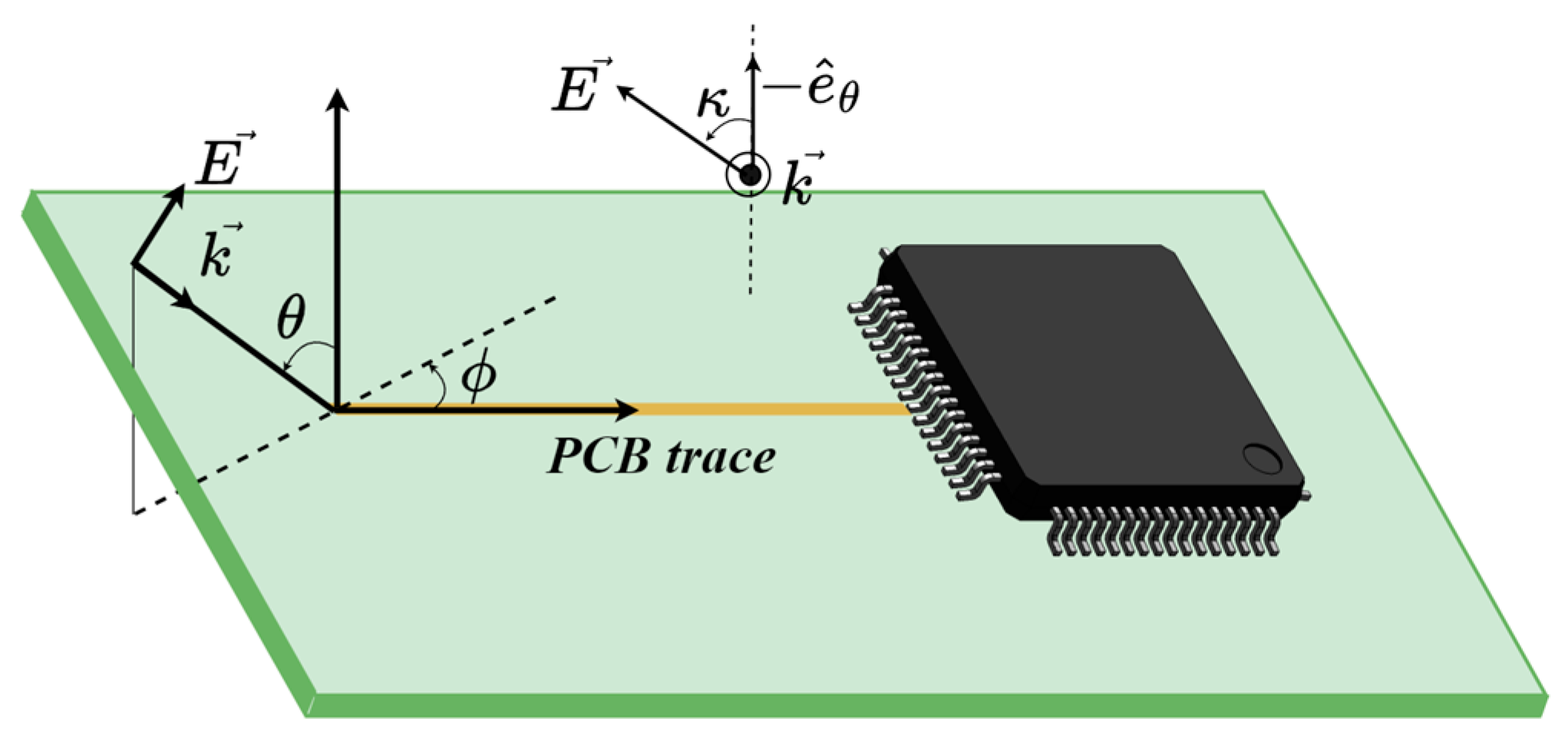
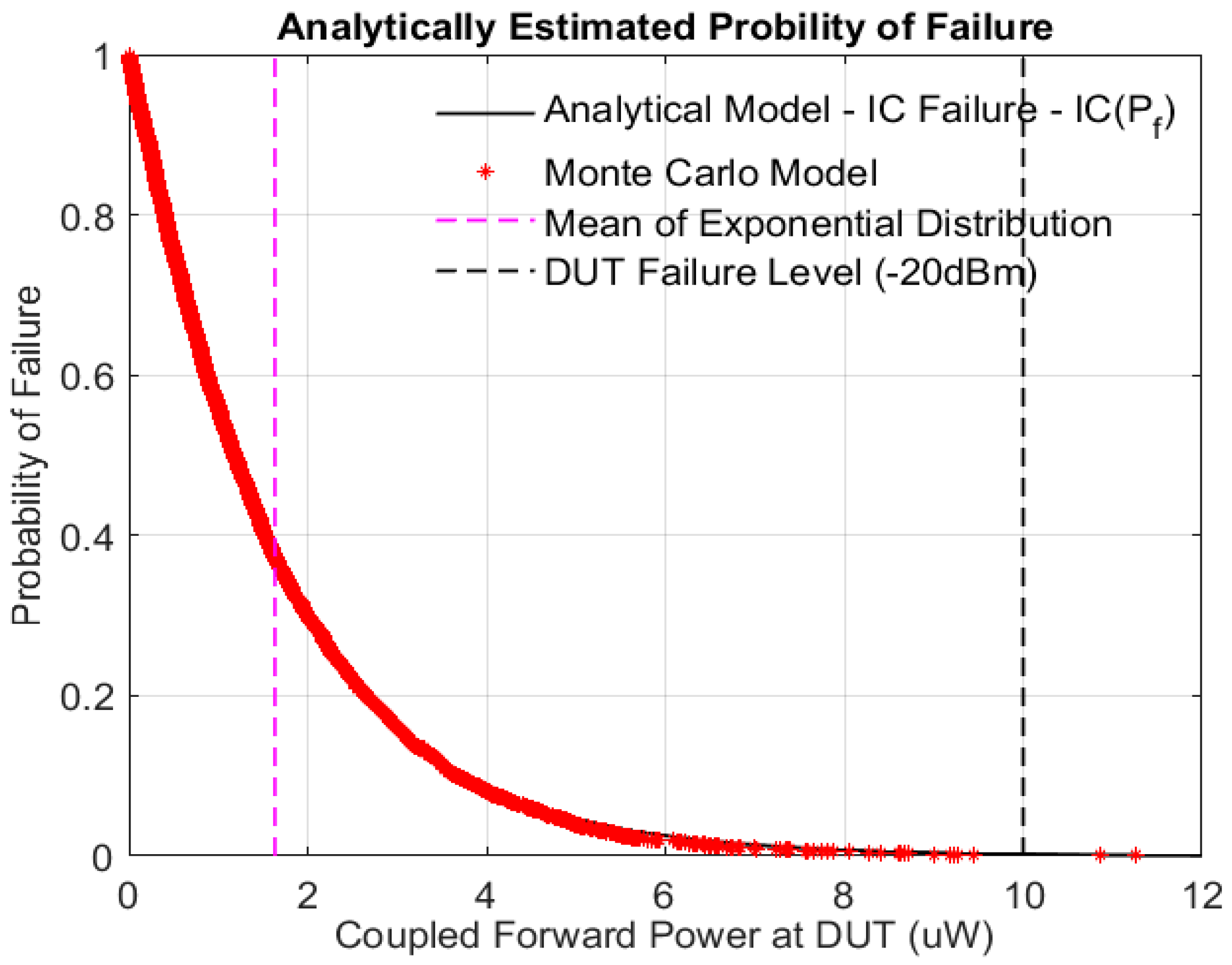
2.2. Analytical Methodology to Predict the Probability of the Susceptibility of ICs

In this section, we introduce an analytical methodology for predicting the probability of IC failure. The method discussed in the previous section allows us to predict the probability density function of the forward power coupled at the end of a lossy PCB trace. The IC EMC standard, IEC 62132-4 [21], facilitates the evaluation of IC immunity by measuring the forward power needed to trigger an IC malfunction.
The Monte Carlo method confirms that the distribution of received forward power is exponential, as would be expected for an antenna in a reverberant environment [22]. The results of the numerical model forward power distribution, along with the analytic exponential distribution with the same variance, can be seen in Figure 2, along with the cumulative distribution in Figure 3.
To gain visual insights into the area under the distribution curve, we use the cumulative distribution function (CDF) of the coupled forward power:
F P f = 1 e λ P f
where P f is the coupled forward power, λ = 1 μ , μ = P f , which is the mean.
Equation (11) provides us with the probability that the power is less than the reference value along the x-axis. The probability of the forward power exceeding the reference value is therefore
I C P f = 1 F P f = e λ P f
In Figure 3, the mean coupled forward power is indicated by a vertical line, and 63.21% of the coupled forward power samples are less than the mean value, while 36.79% exceed it.
Whilst the analytic exponential distribution extends to infinity in a practical evaluation with a finite number of samples, the maximum forward power is likely to be around 10 dB greater than the mean for 100 samples [23]. Therefore, in any practical evaluation of failures, the mean forward power coupled should be large enough to ensure a meaningful number of failures are seen and certainly not more than 10 dB below the failure level. As can be seen from Figure 3, if the mean coupled forward power is equal to the failure power, an actual failure will occur in about 36% of the tests.

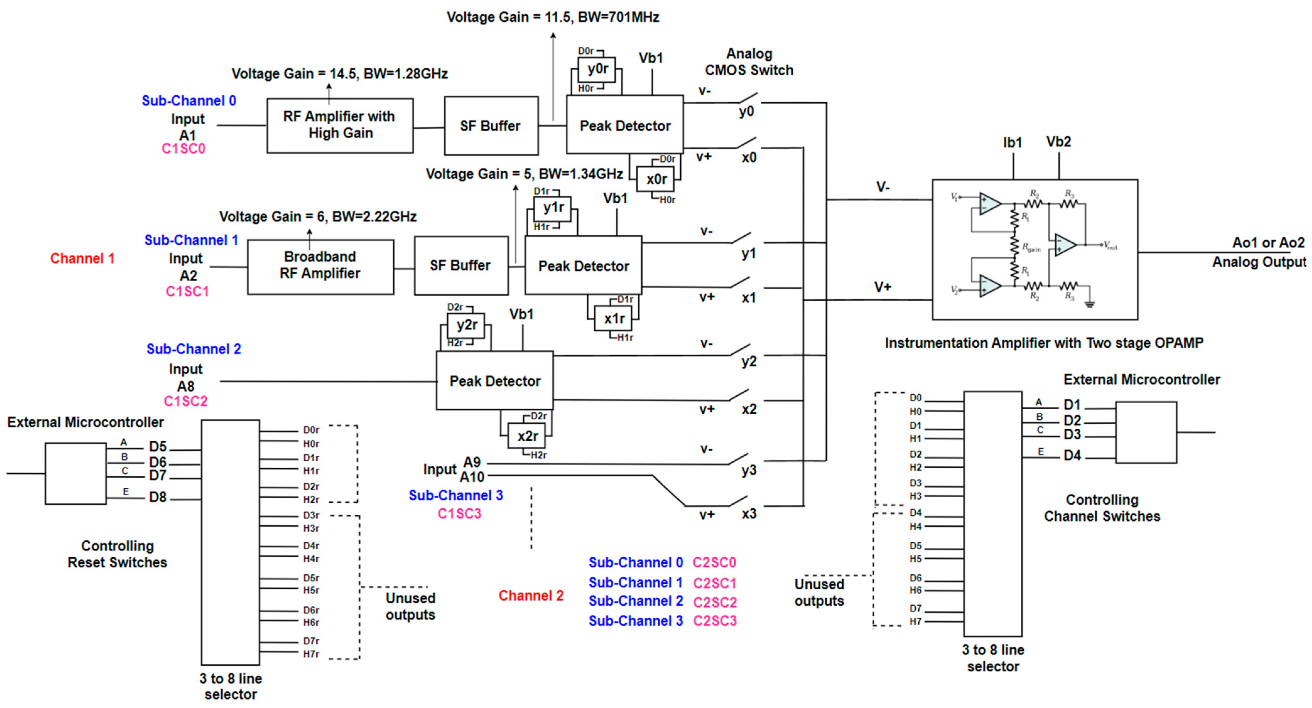
3. Custom RF IC Detector

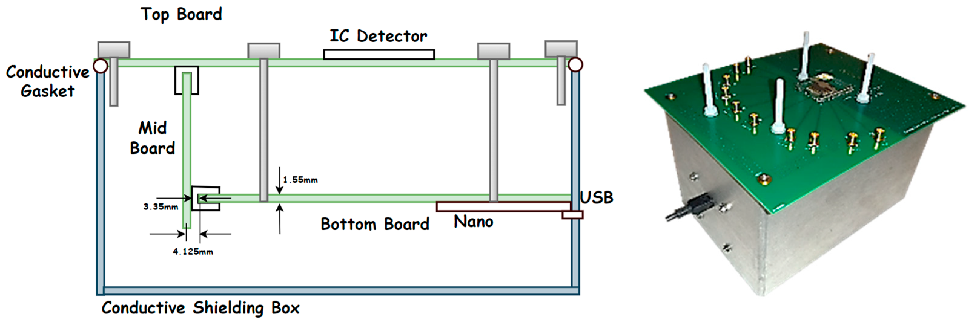
3.1. Introduction and Working Principles of the RF IC Detector

A specialized RF IC detector was designed to quantify the coupled forward power at package pins via test PCB tracks during radiated tests to validate the numerical method from Section 2. The RF IC detector has two channels (C1 and C2), as shown in Figure 4, each with four sub-channels (SC0, SC1, SC2, and SC3), as shown in Figure 4. SC0–SC3 of C2 have identical input circuits to C1 but with a series protection resistance of 100 Ω in the IO block, whereas channel 1 has a low series protection resistance (<1 Ω). The channels connect via an analog multiplexer to a differential instrumentation amplifier and then to a high series resistance (1 kΩ) analog output pin. SC0 has a high-gain RF amplifier, SC1 has a broadband RF amplifier, SC2 is directly connected to the peak detector, and SC3 has two inputs that connect directly to the instrumentation amplifier. The analog multiplexer is controlled by a 3- to 8-line decoder, which receives control signals from an external microcontroller. The detectors have a shorting reset switch across the output capacitor, which is controlled by a separate 3- to 8-line decoder.

3.2. PCB Test Bench for RF IC Detector Characterization

Figure 5 shows the interconnection between the RF IC detector and subsequent blocks for digital control, voltage regulation, bias voltage provision, and output signal amplification. Figure 6 shows the physical layout of the detector (top) and control (bottom) boards. The three interconnected boards (top, middle, and bottom) use a PCIe connector. The top board houses the RF IC detector connected to MCX RF connectors via PCB tracks.
As shown in Figure 6, the middle board serves as a connector between the top and bottom control boards, facilitating communication and data transfer via the PCIe connector. The bottom control board is centered around an Arduino Nano [24] microcontroller, a dual 12-bit digital-to-analog converter (DAC) providing adjustable bias voltages, and a programmable gain amplifier with an 8-channel input multiplexer that allows the Arduino to measure the detector IC channel outputs and other critical bias and operating voltages, along with a voltage regulator and other utility components.

3.3. Radiated Susceptibility of the PCB Test Bench

Radiated immunity measurements were performed within a reverberation chamber at the UoY, where the radiated board was positioned at the top of the test bench. The entire test bench, including the bottom control board, middle board, and the bottom side of the radiated board, is shielded. Only the top side of the radiated board is exposed to the reverberant environment. The ground planes of the top PCB are connected to the metal enclosure by a conductive gasket, as shown in Figure 6 and Figure 7, to ensure that the middle and bottom boards are shielded.
The top side of the radiated board consists of the RF IC detector and RF PCB tracks, which have a characteristic impedance of 115 Ω and are connected to each inputs SC0–SC3 of C1 and C2 of the detector IC. A 65   Ω resistor is inserted between each track end and an MCX connector, so a standard 50   Ω load or instrument can be used to provide a matched termination for each track when required. A track impedance of 115   Ω was chosen, as it is a reasonable value representative of typical circuits, both in cases where matching is not used and in many where it is. Table 1 provides an overview of the radiated board PCB parameters.

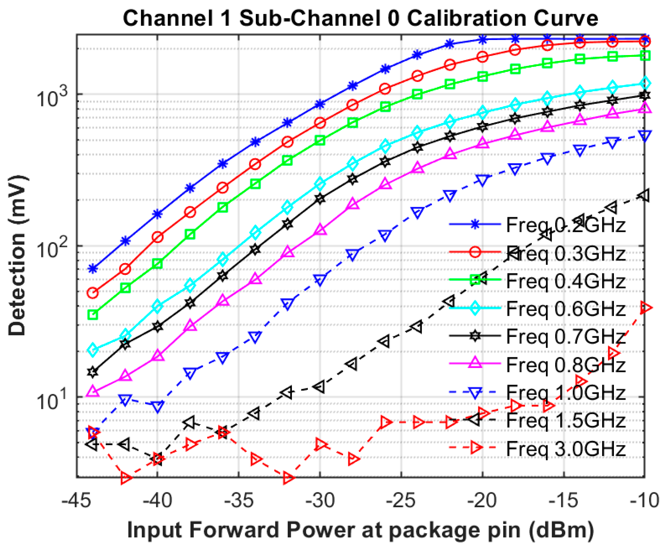
3.4. Calibration of the RF IC Detector Test Bench for Radiated Measurements

Figure 8 presents calibration curves for SC0 of C1. A separate conducted test board with standard 50   Ω PCB traces connected between the MCX connectors and the package pins was built to develop the calibration map for radiated measurements. After calibrating a Rhode & Schwarz vector network analyzer (VNA) from UoY to place the reference plane at the detector pin, by using a custom-built Through-Reflect-Line/Match (TRL/M) calibration board, we injected various known forward power levels at the package pin across the operating frequency band. This procedure facilitated the creation of a calibration map for radiated measurements using the RF IC detector. Integrating these calibration curves from all sub-channels into python software (2.7.16) during the radiated measurements enabled the determination of the coupled forward power at the package pin from the detector output voltage.

4. Experimental Validation of Stochastic EM-Field Coupling into PCB Traces

The validation process involved conducting radiated coupling measurements within a reverberation chamber (Figure 9), utilizing the RF IC detector test bench described above.

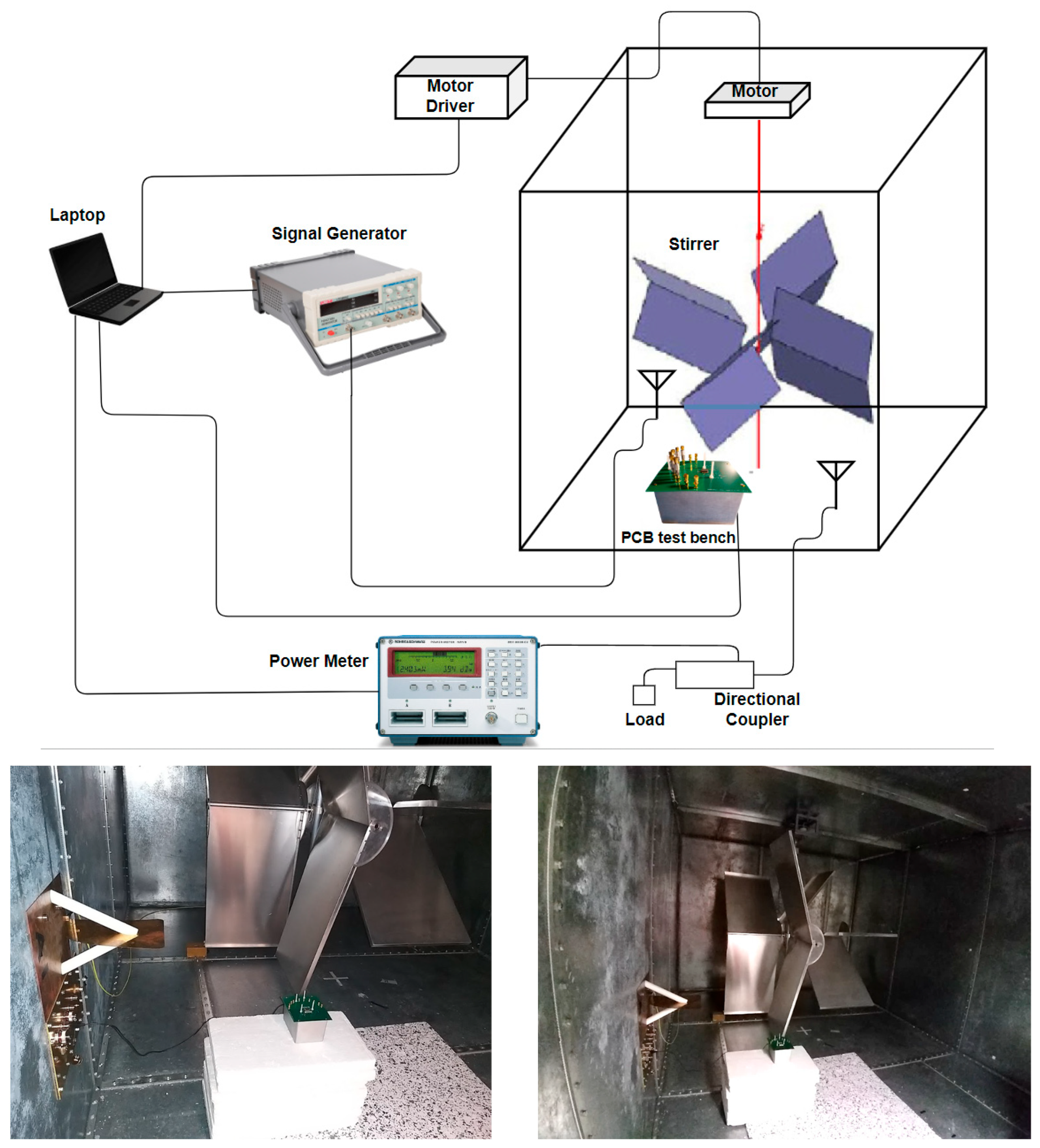
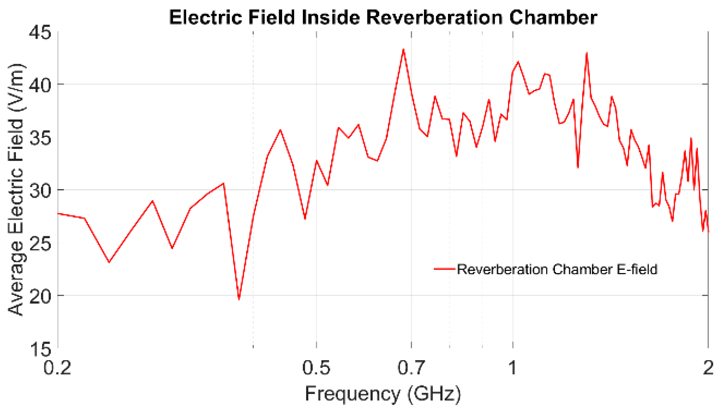
4.1. Measurement Setup

The measurements are conducted for 100 stirrer positions from 200 MHz to 2 GHz with a 20 MHz step. A power signal generator drives a broadband antenna to generate the field in the chamber, which is monitored by measuring the power received by a second broadband antenna. Coupling to each detector channel is measured by the test bench and transmitted to the instrument controller by the USB interface of the Arduino board.
From the received power, averaged over a number of stirrer positions, P r , we can deduce the chamber total field:
E 0 2 = 8 π Z o λ 2 P r = 8 π Z o λ 2 P P M T c 2 1 Γ a 2 η 2
where Z o = μ O / ε O represents the free space impedance, λ is the free space wavelength, P P M represents the received power measured by the power meter at the receiving antenna, T c denotes the transmission coefficient of the cable connected between the receiving antenna and the power meter, η 2 is the antenna efficiency of the receiving antenna, and Γ a represents the reflection voltage coefficient of the receiving antenna at the respective stirrer position. The total E-field ( E 0 ) level inside the reverberation chamber for a forward power of 29 dBm at the transmitting antenna is shown in Figure 10.
To test the immunity characteristics of the RF IC detector, we conducted measurements with and without shielding over the IC package. This showed only a small difference in the detected power and demonstrated that coupling via the IC package was negligible compared to coupling via the PCB trace.

4.2. Coupled Forward Power at the Package Pin

For the results in this paper, the terminating ends of the PCB track that connect to all sub-channels of the RF IC detector are left open. This results in an increase in the coupled forward power at the package pin compared to a matched load, which improves the sensitivity of the measurement.
At each stirrer position and frequency point, the coupled forward power at the package pin is detected by SC0 to SC2 of C1 and C2 of the RF IC detector.

Average Coupled Forward Power at the Package Pin

The average coupled forward power at the package pins for SC2 of C1 and C2 is shown in Figure 11 with solid lines for a forward power of 29 dBm at the transmitting antenna. The minimum forward power level required for the RF IC detector to detect at least a 10 mV output voltage is shown by dashed lines.
We validate the Monte Carlo method discussed in Section 2.1 by comparing our results with the numerical model based on the Monte Carlo method. In the numerical model, we incorporated the input impedance of the respective sub-channel at the IC end. At the other end of the track, we applied an impedance of 10   G to resemble the open circuit scenario of the test bench. Additionally, we integrated all the dielectric properties of the radiated board from Table 1 into the numerical model to derive the curve.
The numerical model curve (black dashed line in Figure 11) closely matches the measurement results from 380 MHz to 700 MHz. We postulate that, below 380 MHz, the measurement results for coupled forward power are at the minimum detection threshold but do not surpass it entirely. Above 700 MHz, the deviation may be attributed to cross-coupling between the traces and package pins, as well as parasitic effects introduced within the dielectric. Additionally, the numerical model assumes an infinite ground plane, which differs from the physical model, potentially contributing to the observed deviation.

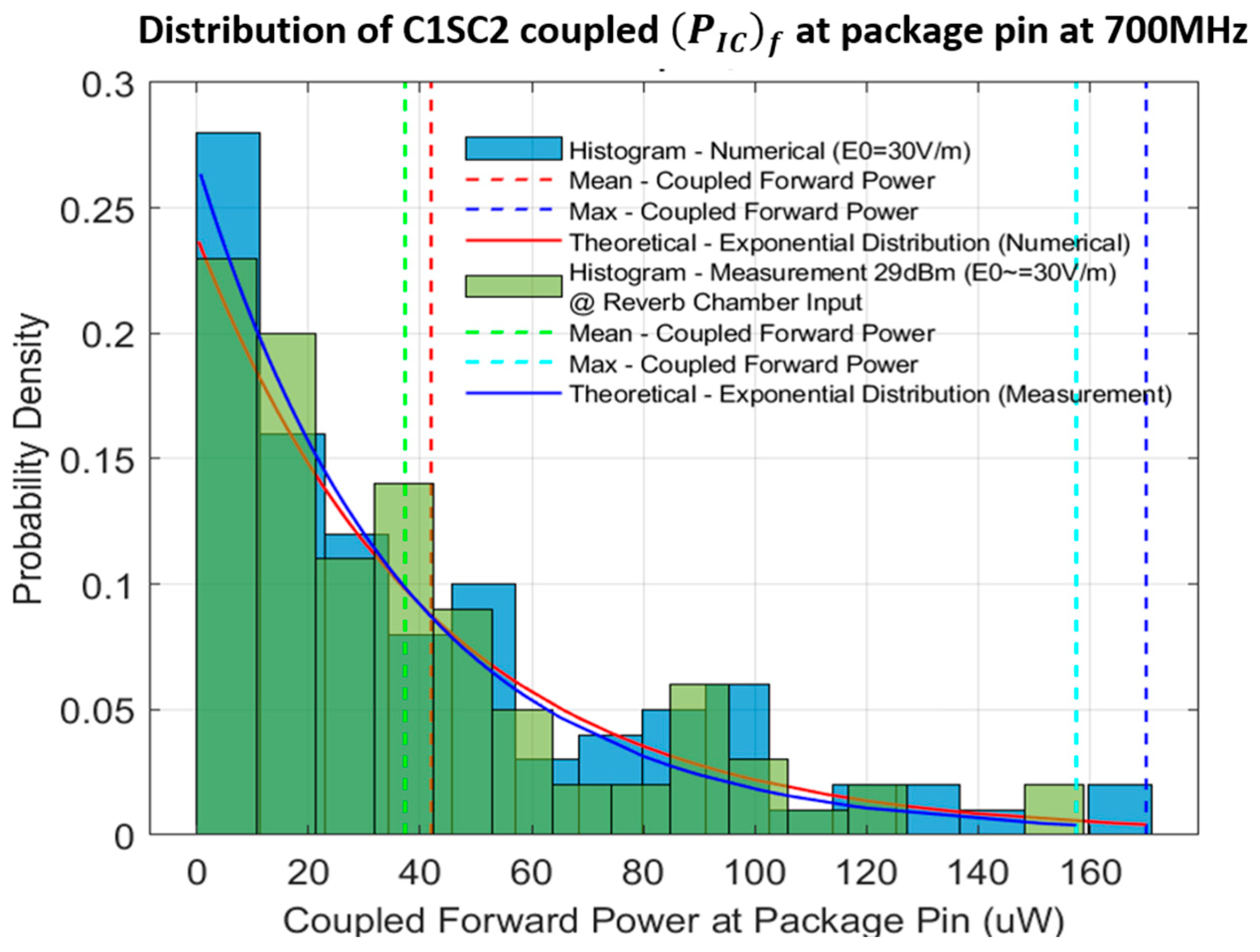
4.3. Coupled Forward Power Distribution at the Package Pin

In Section 2.1, we determined that the distribution of the coupled forward power at the package is expected to be exponential (Figure 2).
In this section, we compare the numerically estimated data with the measurement results of one of the sub-channels (C1SC2) in Figure 12. The measurement results align well with the numerically estimated data.

5. Correlating Prediction Models with Practical Applications

5.1. Correlating with Test Specifications of EMC Limits for Automotive ICs

In this section, we aim to bridge the gap between theoretical insights and practical applications by establishing a correlation between the test specifications of EMC limits for automotive ICs and our prediction models.
The EMC limits for automotive ICs, pertaining to conducted immunity (direct power injection (DPI)) and radiated immunity (GTEM and IC stripline), are outlined in Section 11.2 of [25] and are also mentioned in [26]. In cases where the coupled forward power to the IC surpasses certain thresholds specified in the EMC limits for DPI, as detailed in the test specifications provided in Table 44 of [25], the IC is prone to malfunction and may meet one of the predefined failure criteria. To establish a connection between the EMC limits for automotive ICs in test specifications and our prediction models, we make use of the general immunity limit classes from these test specifications.
Conducting radiated immunity tests in a reverberation chamber offers a more realistic approximation of complex real-world electromagnetic environments than conventional methods such as GTEM cells or IC stripline setups, which are typically limited to fixed directions and polarizations. In contrast, a reverberation chamber generates a statistically isotropic, randomly polarized field, simulating the multipath and spatial variability often encountered in practical EMI scenarios. Because the energy is incident on the DUT from all directions and with all polarizations, the chamber enables the identification of worst-case coupling conditions. Hence, we increase the E-field in the numerical model in such a way that all the DPI limit lines from [25] fall within the estimated distribution range of the coupled forward power at the local IC package pin, and then, we plot the analytically estimated probability of IC failure curve calculated using Equation (12) with respect to the numerically estimated coupled forward power, as demonstrated in Figure 13. This gives us the visual representation of the probability of IC failure when the IC under testing belongs to Class I, II, or III, as detailed in Table 2.

5.2. Correlating with Everyday Electronic Appliances

Let us assume we have a DUT connected to a PCB track with known dielectric properties and track parameters, categorized as a Class B digital device according to standard FCC 47 CFR Part 15 [27], which includes DUTs from personal computers, calculators, and similar electronic devices. If the DUT has a failure level of −20 dBm, it will exhibit a 99.98% probability of failure when exposed to an 80 V/m E-field in a reverberant environment, as shown in Figure 14.
To achieve an acceptable probability of failure, i.e., 0.02% (2 in 10,000 samples), we need nearly 13 times less E-field (6 V/m) around the DUT compared to the E-field required for a 99.98% probability of failure, as illustrated in Figure 15. This type of estimation is straightforward using our prediction models, as performing real measurements with 10,000 stirrer positions in a reverberation chamber is challenging and time-consuming.

6. Discussion

The method presented in this work demonstrates a practical approach to predicting the susceptibility of PCB-mounted components to EMI in reverberant environments. By combining a known susceptibility threshold (e.g., per IEC 62132-4) with the statistical behavior of coupled forward power, a probability of failure for the device under test (DUT) can be quantitatively estimated.
The experiments conducted using the custom RF IC detector validated the numerical predictions well, highlighting the relevance of the model even with practical PCB designs. The consistency between the measured and predicted forward power distributions provides confidence in applying the method for early-stage EMC risk assessments without relying solely on extensive testing. Furthermore, the flexibility of the approach suggests that it could be extended beyond ICs to other sensitive PCB sub-circuits or discrete components, as long as their susceptibility thresholds are known.
A key assumption made in this work is that the reverberant field can approximate realistic EMI conditions. As discussed earlier, although real-world environments involve both deterministic and stochastic components, studies have shown that properly stirred reverberation chambers provide statistically representative fields comparable to many practical EMI scenarios, particularly for immunity and susceptibility testing. Thus, the results from such controlled environments can be reasonably extrapolated to real-world conditions, provided the incident field statistics are well characterized [5]. The prediction methodology presented here thus lays a strong foundation for extending the concept to realistic EMI exposure.

7. Conclusions and Future Work

In this paper, the proposed susceptibility prediction method provides a probability of failure value when the component failure level is within the distribution range of coupled forward power for any PCB component attached to a PCB track. We have presented and, through experiments, we have validated a model to predict the forward power coupled by an exposed PCB track into an IC pin in a reverberant environment. The known coupling statistics of reverberation chambers allow us to therefore estimate the probability of failure of a component, subjected to a known mean field strength if we know the forward power level at which the device is susceptible, as measured according to the IEC 62132-4 standard or similar method. We believe this concept is also applicable to real-world applications where single or multiple interfering sources may illuminate an equipment.
Furthermore, we established a correlation between the practical applications and our prediction models where we estimated the acceptable E-field around the DUT to obtain an acceptable probability of DUT failure. The proposed methodology for estimating the probability of susceptibility of ICs (DUTs) in this paper holds significant value for the EMC community, providing a more accurate estimation of the probability of the susceptibility of ICs.
Incorporating PCB losses into the numerical model results in a difference of less than 0.6 dB throughout the operating frequency range, as shown in Figure 16. However, we believe that the losses might become significant above 3 GHz, where our updated numerical model, which accounts for losses, could provide further insights. This could be explored in future works. Additionally, enhancing the numerical model to estimate stochastic EM coupling into PCB traces, considering cross-couplings, and studying closely spaced PCB tracks and their average absorption cross-section (AACS) are potential areas for future exploration.

Author Contributions

Conceptualization, A.H.V., J.F.D., M.A.T., H.X., S.J.B., A.C.M. and M.P.R.; methodology, A.H.V., J.F.D., M.A.T., H.X., S.J.B. and A.C.M.; software, A.H.V. and J.F.D.; validation, A.H.V.; formal analysis, A.H.V. and A.C.M.; investigation, A.H.V., J.F.D., M.A.T. and H.X.; resources, J.F.D. and A.C.M.; writing—original draft, A.H.V.; writing—review and editing, J.F.D., M.A.T., S.J.B., A.C.M. and M.P.R.; supervision, J.F.D., M.A.T., S.J.B., A.C.M. and M.P.R.; project administration, J.F.D. and M.A.T.; funding acquisition, J.F.D. and M.A.T. All authors have read and agreed to the published version of the manuscript.

Funding

The research leading to these results received funding from the European Union’s Horizon 2020 Research and Innovation Programme under the Marie Skłodowska-Curie grant agreement No. 812790 (MSCA-ETN PETER). This publication reflects only the authors’ views, and the European Union is not responsible for any use that may be made of the information it contains. Project website: http://etn-peter.eu/.

Data Availability Statement

The original contributions presented in this study are included within the article. Further inquiries can be directed to the corresponding author.

Acknowledgments

The authors sincerely appreciate the valuable comments and efforts of the reviewers and editors on this article.

Conflicts of Interest

The authors declare no conflicts of interest.

Abbreviations

The following abbreviations are used in this manuscript:
AACSAverage Absorption Cross-Section
BLTBaum–Liu–Tesche
CDFCumulative Distribution Function
C1SC2Channel 1 Sub-channel 2
DACDigital-to-Analog Converter
DPIDirect Power Injection
DUTDevice Under Test
EMElectromagnetic
EMCElectromagnetic Compatibility
EMIElectromagnetic Interference
EUTEquipment Under Test
GTEMGigahertz Transverse Electromagnetic
ICIntegrated Circuits
MCMonte Carlo
PCBPrinted Circuit Board
RF ICRadio Frequency Integrated Circuit
TETransverse Electric
TMTransverse Magnetic
TRL/MThrough-Reflect-Line/Match
UoYUniversity of York
VNAVector Network Analyzer

References

  1. Konefal, T.; Marvin, A.C.; Dawson, J.F.; Robinson, M.P. A Statistical Model to Estimate an Upper Bound on the Probability of Failure of a System Installed on an Irradiated Vehicle. IEEE Trans. Electromagn. Compat. 2007, 49, 840–848. [Google Scholar] [CrossRef]
  2. Mehri, M.; Masoumi, N. Statistical Prediction and Quantification of Radiated Susceptibility for Electronic Systems PCB in Electromagnetic Polluted Environments. IEEE Trans. Electromagn. Compat. 2017, 59, 498–508. [Google Scholar] [CrossRef]
  3. Perdriau, R.; Ramdani, M.; Maurice, O.; Dubois, S.; Sicard, E. Assessment of the Radiated Immunity of Integrated Circuits in the 3–40 GHz Range. In Proceedings of the 2011 8th Workshop on Electromagnetic Compatibility of Integrated Circuits, Dubrovnik, Croatia, 6–9 November 2011; pp. 18–23. [Google Scholar]
  4. Heinrich, R.; Bechly, R.; Deutschmann, B. Radiated Immunity Testing of Integrated Circuits in Reverberation Chambers. In Proceedings of the International Symposium on Electromagnetic Compatibility—EMC EUROPE, Rome, Italy, 17–21 September 2012; pp. 1–4. [Google Scholar]
  5. BS EN 61000-4-21; Testing and Measurement Techniques—Reverberation Chamber Test Methods. BSI Standards Publication: London, UK, 2011.
  6. Hwang, J.; Han, Y.; Park, H.; Nah, W.; Kim, S. Radiated Electromagnetic Immunity Analysis of VCO Using IC Stripline Method. In Proceedings of the 2015 10th International Workshop on the Electromagnetic Compatibility of Integrated Circuits (EMC Compo), Edinburgh, UK, 10–13 November 2015; pp. 147–151. [Google Scholar]
  7. Boyer, A.; Nolhier, N.; Caignet, F.; Dhia, S.B. Correlation between Near-Field Scan Immunity and Radiated Susceptibility at Integrated Circuit Level. In Proceedings of the 2022 International Symposium on Electromagnetic Compatibility—EMC Europe, Gothenburg, Sweden, 5–8 September 2022; pp. 120–125. [Google Scholar]
  8. Koohestani, M.; Perdriau, R.; Ramdani, M. An Effective Approach to Mitigate IC Radiated Susceptibility in EM Far-Field Region. In Proceedings of the 2019 International Symposium on Electromagnetic Compatibility—EMC EUROPE, Barcelona, Spain, 2–6 September 2019; pp. 144–148. [Google Scholar]
  9. Xie, H.; Dawson, J.F.; Yan, J.; Marvin, A.C.; Robinson, M.P. Numerical and Analytical Analysis of Stochastic Electromagnetic Fields Coupling to a Printed Circuit Board Trace. IEEE Trans. Electromagn. Compat. 2020, 62, 1128–1135. [Google Scholar] [CrossRef]
  10. Venkateshaiah, A.H.; Xie, H.; Dawson, J.F.; Marvin, A.C.; Dawson, L.; Robinson, M.P. Coupling of Energy Into PCB Traces in a Reverberant Environment: Absorption Cross-section and Probability of Susceptibility. In Proceedings of the 2020 International Symposium on Electromagnetic Compatibility—EMC EUROPE, Rome, Italy, 23–25 September 2020; pp. 1–6. [Google Scholar]
  11. Tang, H.H.; Venkateshaiah, A.F.; Dawson, J.F.; Marvin, A.C.; Robinson, M.P.; Ge, J. Analysis and Estimation of Electromagnetic Energy Coupled into IC packages. In Proceedings of the 2021 Joint IEEE International Symposium on Electromagnetic Compatibility, Signal and Power Integrity, EMC Europe, Raleigh, NC, USA, 26 July–13 August 2021. [Google Scholar]
  12. Tesche, F.M.; Butler, C.M. On the addition of EM field propagation and coupling effects in the BLT equation. Interact. Notes 2003, 588, 1–43. [Google Scholar]
  13. Tesche, F.M.; Ianoz, M.; Karlsson, T. EMC Analysis Methods and Computational Models; John Wiley & Sons: Hoboken, NJ, USA, 1996. [Google Scholar]
  14. Hall, S.; Pytel, S.G.; Huray, P.G.; Hua, D.; Moonshiram, A.; Brist, G.A.; Sijercic, E. Multigigahertz Causal Transmission Line Modeling Methodology Using a 3-D Hemispherical Surface Roughness Approach. IEEE Trans. Microw. Theory Tech. 2007, 55, 2614–2624. [Google Scholar] [CrossRef]
  15. Zhang, J.; Koledintseva, M.Y.; Drewniak, J.L.; Pommerenke, D.J.; DuBroff, R.E.; Yang, Z.; Cheng, W.; Rozanov, K.N.; Antonini, G.; Orlandi, A. Reconstruction of Dispersive Dielectric Properties for PCB Substrates Using a Genetic Algorithm. IEEE Trans. Electromagn. Compat. 2008, 50, 704–714. [Google Scholar] [CrossRef]
  16. IS400, FR4. Substrate, Eurocircuits. Available online: https://www.isola-group.com/wp-content/uploads/data-sheets/is400-laminate-and-prepreg-isola-group.pdf?t=1822223916 (accessed on 25 May 2025).
  17. Koledintseva, M.Y.; Rozanov, K.N.; Orlandi, A.; Drewniak, J.L. Extraction of Lorentzian and Debye Parameters of Dielectric and Magnetic Dispersive Materials for FDTD Modeling. J. Electr. Eng. 2002, 53, 97–100. [Google Scholar]
  18. Sohn, Y.-S.; Lee, J.-C.; Park, H.-J.; Cho, S.-I. Empirical equations on electrical parameters of coupled microstrip lines for crosstalk estimation in printed circuit board. IEEE Trans. Adv. Packag. 2001, 24, 521–527. [Google Scholar] [CrossRef]
  19. Leone, M.; Singer, H.L. On the coupling of an external electromagnetic field to a printed circuit board trace. IEEE Trans. Electromagn. Compat. 1999, 41, 418–424. [Google Scholar] [CrossRef]
  20. Magdowski, M.; Tkachenko, S.V.; Vick, R. Coupling of Stochastic Electromagnetic Fields to a Transmission Line in a Reverberation Chamber. IEEE Trans. Electromagn. Compat. 2011, 53, 308–317. [Google Scholar] [CrossRef]
  21. BS EN 62132-4; Integrated Circuits—Measurement of Electromagnetic Immunity 150 kHz to 1 GHz Part 4, Direct RF Power Injection Method. BSI Standards Publication: London, UK, 2006.
  22. Hill, D.A. Plane Wave Integral Representation for Fields in Reverberation Chambers. IEEE Trans. Electromagn. Compat. 1998, 40, 209–217. [Google Scholar] [CrossRef]
  23. Wellander, N.; Lunden, O.; Backstrom, M. The Maximum Value Distribution in a Reverberation Chamber. In Proceedings of the 2001 IEEE EMC International Symposium. Symposium Record. International Symposium on Electromagnetic Compatibility (Cat. No. 01CH37161), Montreal, QC, Canada, 13–17 August 2001; Volume 2, pp. 2751–2756. [Google Scholar]
  24. Arduino Nano (V2.3) User Manual. 2008. Available online: https://www.arduino.cc/en/uploads/Main/ArduinoNanoManual23.pdf (accessed on 25 May 2025).
  25. Elektroindustrei, Z.D. Generic IC EMC Test Specification; Version 2.1; ZVEI—German Electrical and Electronic Manufacturers’ Association: Frankfurt am Main, Germany, 2017; Available online: https://www.zvei.org/presse-medien/publikationen/leitfaden-generic-ic-emc-test-specification-version-21 (accessed on 25 May 2025).
  26. Klotz, F. EMC Test Specification for Integrated Circuits. In Proceedings of the 2007 18th International Zurich Symposium on Electromagnetic Compatibility, Munich, Germany, 24–28 September 2007; pp. 73–78. [Google Scholar]
  27. FCC Part 15, U.S. EMC Standard. Available online: https://www.academyofemc.com/emc-standards (accessed on 25 May 2025).
Figure 2. Numerically estimated coupled forward power distribution at the package pin ( Z I C of C1SC2, 700 MHz and 1200 MHz), analyzed with B = 100 boundary conditions and N = 100 plane waves.
Electronics 14 02187 g002
Figure 3. Numerically estimated cumulative distribution of the coupled forward power at the package pin (C1SC2, 700 MHz and 1200 MHz). Aggregated data with B = 100 samples, showcasing the cumulative distribution of power coupling at the package pin.
Electronics 14 02187 g003
Figure 4. Block diagram depicting RF IC detector functionality and structure.
Electronics 14 02187 g004
Figure 5. Concise block diagram of the PCB test bench setup.
Electronics 14 02187 g005
Figure 6. (Left) The integrated PCB test bench with interconnected PCBs for a comprehensive system evaluation. (right) The assembled test setup featuring the radiated PCB at the top.
Electronics 14 02187 g006
Figure 7. To ensure proper grounding for the shielding, a grounded conducting path in a rectangular configuration is incorporated on the underside of the top board.
Electronics 14 02187 g007
Figure 8. Calibration curve that displays the relationship between input forward power at the package pin and detector output voltage for C1 SC0 at different frequency points.
Electronics 14 02187 g008
Figure 9. Measurement setup and images of the reverberation chamber with a test bench.
Electronics 14 02187 g009
Figure 10. Shows the total E-field inside the reverberation chamber for 100 stirrer positions when 29 dBm of forward power is given to the transmitting antenna of the chamber.
Electronics 14 02187 g010
Figure 11. Coupled average forward power at the package pin with open tracks when 29 dBm of forward power is supplied to the transmitting antenna of the chamber.
Electronics 14 02187 g011
Figure 12. Distribution of coupled forward power at the package pin (C1 SC2, 700 MHz): Over 100 stirrer positions are analyzed, depicting variations in power coupling at the package pin in measurement and numerically estimated data.
Electronics 14 02187 g012
Figure 13. Predicting the probability of IC failure with respect to numerically estimated coupled forward power at local IC pin (C1SC2) for 400 V/m E-field at 700 MHz. From the DPI limit line set for the local pin, we can determine the probability of IC failure if the IC under test belongs to Class I, II or III.
Electronics 14 02187 g013
Figure 14. Predicting the probability of IC failure with respect to numerically estimated coupled forward power at the DUT for 80 V/m E-field at 700 MHz for B = 10,000 samples.
Electronics 14 02187 g014
Figure 15. Predicting the probability of IC failure with respect to numerically estimated coupled forward power at the DUT for 6 V/m E-field at 700 MHz for B = 10,000 samples.
Electronics 14 02187 g015
Figure 16. Shows the difference between the numerically estimated coupled average forward power at the package pin (C1-SC0) via lossless and lossy PCB traces.
Electronics 14 02187 g016
Table 1. Radiated PCB parameters are shown.
Parameter NameRadiated Board
Number of Layers4
RF PCB track width (w)0.48 mm
RF PCB track thickness (t)18 μm
Substrate height from ground plane for RF PCB tracks (h)1.43 mm
Characteristic Impedance of the RF PCB Track115 Ω
Board Dimension 180 × 153 mm2
Coefficient for the Roughness Effect ( K r ) [Calculated using Equation (5)]2.2 @700 MHz
Dielectric Constant (Dk)/Relative Permittivity ( ε r )(FR4-improved, IS400) [16]
4.0 @100 MHz
3.9 @500 MHz
Diffraction Factor (Df)/Loss Tangent ( t a n δ )0.020 @100 MHz
0.022 @500 MHz
Table 2. The probability of IC failure if the IC under testing belongs to Class I, II, or III for the given E-Field at 700 MHz.
Local Pin C1SC2 at 700 MHz for 400 V/m
If the IC Under Testing Belongs to the ClassThen the Probability of IC Failure Is
ClassLimit Lines
I0 dBm88.00%
II6 dBm59.97%
III12 dBm12.96%
Disclaimer/Publisher’s Note: The statements, opinions and data contained in all publications are solely those of the individual author(s) and contributor(s) and not of MDPI and/or the editor(s). MDPI and/or the editor(s) disclaim responsibility for any injury to people or property resulting from any ideas, methods, instructions or products referred to in the content.

