1. Introduction
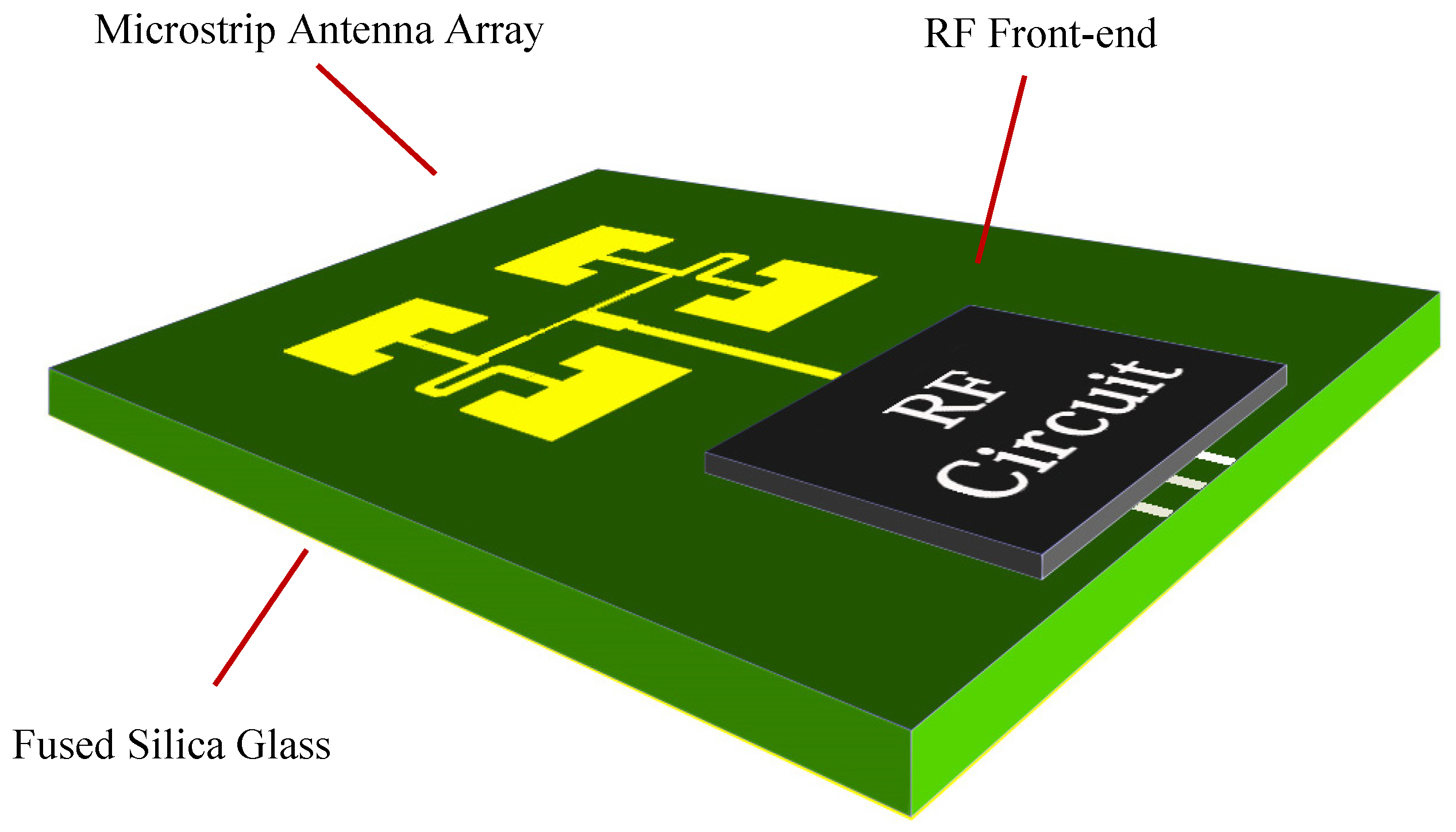
The rapid advancement of millimeter-wave (30–300 GHz) and terahertz (0.1–10 THz) technologies has positioned on-chip microstrip antenna arrays (
Figure 1) as critical components in high-frequency integrated systems. Compared to traditional discrete antennas, these arrays offer significant advantages, including reduced packaging complexity, minimized interconnection losses through direct integration into semiconductor substrates, and inherent benefits such as low cost, low profile, and high consistency. These attributes make them ideal for compact radio-frequency front-ends in applications spanning millimeter-wave radar, 5G/6G communications, and high-speed wireless data transmission [
1,
2,
3].
Despite these advantages, the practical deployment of on-chip microstrip antenna arrays faces substantial challenges. First, conventional substrate materials (e.g., silicon and GaAs) exhibit high dielectric loss tangents (tan δ > 0.01) and pronounced parasitic coupling effects at high frequencies, severely degrading radiation efficiency. This results in limited gain and narrow operational bandwidth. For instance, prior studies on 2 × 2 on-chip arrays demonstrated modest gains of 6.75 dBi [
4], 8.5 dBi [
5], and 6.9 dBi [
6] on silicon and GaAs substrates, while a 94 GHz silicon-based array achieved a bandwidth of only 1 GHz [
7]. Second, existing designs often employ complex fabrication techniques—such as through silicon vias (TSVs) or multilayer stacking to mitigate surface wave losses, which escalate manufacturing costs and compromise reliability [
8]. Finally, performance inconsistencies caused by substrate material variations further hinder the scalability of millimeter-wave and terahertz on-chip antenna arrays [
9,
10].
To address these challenges, fused silica glass emerges as a promising solution due to their exceptional high-frequency properties. With an ultra-low loss tangent (tan δ < 0.001 at 77 GHz) and stable dielectric constant (ε
r ≈ 3.9), the fused silica glass significantly mitigates substrate losses and suppresses surface wave excitation, thereby enhancing gain and radiation efficiency [
11]. Additionally, its isotropic mechanical and thermal stability ensure excellent agreement between simulated and measured antenna parameters in millimeter-wave bands—a critical advantage for high-precision, low-loss designs [
12]. However, the performance of such arrays remains constrained by two critical challenges: feed network losses persist as a dominant efficiency bottleneck in array architectures, while simultaneously achieving broadband operation and high gain requires innovative design trade-offs.
This paper presents a W-band 2 × 2 on-chip antenna array fabricated on a fused silica glass, offering a cost-effective solution for millimeter-wave systems. The key contributions include the adoption of an embedded feeding structure and T-junction power dividers to minimize feedline losses while extending impedance-matching bandwidth, the integration of ultra-low-loss fused silica glass with 500 nm gold microstrip lines to mitigate conductor losses caused by skin effects, and the co-optimization of radiating elements and feed networks to achieve broadband high-gain performance across 76.11–83.87 GHz. These advancements collectively address critical challenges in high-frequency on-chip antenna design, demonstrating significant potential for applications in 6G communications and automotive radar.
2. Antenna Array Design
2.1. Antenna Unit Design
The proposed antenna employs a fused silica glass as its dielectric substrate, and a comprehensive analysis of properties and cost for common antenna substrates is detailed in
Table 1. Boasting an exceptionally low dielectric constant and an extremely low tangent of loss angle, the glass demonstrates a remarkable performance in high-frequency antenna applications by significantly reducing energy dissipation while maintaining superior radiation efficiency. Compared to alternative substrates with equivalent high-frequency capabilities such as sapphire and Rogers 5880, it presents an incomparable economic advantage due to its substantially lower fabrication costs (reduced by 95% and 20%). Moreover, the substrate’s exceptionally low coefficient of thermal expansion ensures minimal susceptibility to temperature variations, rendering it ideally suited for deployment in complex environmental conditions. The glass substrate has an ultralow dielectric loss, stable permittivity, and competitive fabrication costs, making it an ideal antenna substrate for mm wave and terahertz applications.
The proposed antenna array utilizes rectangular patch elements as its fundamental radiating units, with their dimensional parameters precisely determined through rigorous microstrip radiation principal calculations, ensuring that the patch length and width satisfy the fundamental design criteria established in Equations (1) and (2), respectively.
where c denotes the vacuum speed of light,
represents the operation frequency of the antenna, and
signifies the effective dielectric constant.
The operation frequency
and effective dielectric constant
are rigorously determined through the analytical solutions presented in Equations (3) and (4).
where
denotes the guided wavelength within the medium,
.
The proposed microstrip patch antenna design features a monolithic glass substrate with an optimized 200 μm thickness for 77 GHz operation, employing a 500 nm thick gold transmission line to suppress the skin depth effects while maintaining radiation efficiency. The antenna’s design parameters, including patch length (L), width (W), and feed line dimensions, were derived through the analytical modeling of electromagnetic wave propagation in dielectric media, as shown in
Table 2.
Microstrip antenna elements inherently suffer from bandwidth constriction and suboptimal gain/directional performance, limitations that can be effectively mitigated through the implementation of embedded feeding mechanisms. These mechanisms introduce additional resonant modes, enhancing bandwidth while optimizing radiation efficiency.
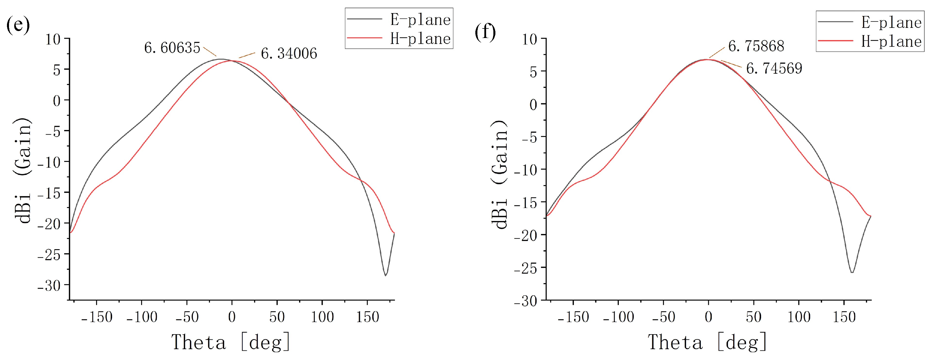
Figure 2a,b provides a comparative schematic of conventional microstrip antenna elements versus their insertion-fed counterparts, highlighting the architectural differences. To evaluate the performance improvements, the reflection coefficients (S11 parameters) and gain radiation patterns in both the E-plane and H-plane were numerically investigated for two distinct microstrip patch antenna configurations using 3D electromagnetic (3D-EM) simulation. The results, illustrated in
Figure 2c–f, demonstrate that the modified structure with the embedded-feed mechanism achieves significant performance enhancements. Specifically, the operational bandwidth satisfying the −10 dB return loss criterion expands from 75.14–78.84 GHz to 75.17–79.17 GHz, representing an absolute bandwidth increase from 3.70 GHz to 4.00 GHz and a relative bandwidth improvement from 4.8% to 5.2%. Furthermore, the radiation patterns exhibit stabilized half-power beamwidths in both the E plane and H plane directions, converging to approximately 83° compared to the original 81–90° angular variation. These results collectively validate the superior operational bandwidth, gain characteristics, and directional stability achieved through the inset feeding strategy in microstrip patch antenna design.
2.2. Antenna Array Construction
Due to the inherent limitations in gain and the directionality of single-element antennas, which fail to meet system requirements, the adoption of an antenna array architecture is essential to achieve the prescribed performance specifications.
The array design targets a gain of 11 ± 1 dBi. Given that each doubling of antenna elements contributes approximately 3 dBi to the overall gain, and considering the single-element peak gain of 6.75 dBi, a four-element configuration is required. To optimize the structural compactness and fabrication simplicity while satisfying performance criteria, a 2 × 2 planar array architecture represents the strategic choice, effectively balancing radiation enhancement with dimensional constraints.
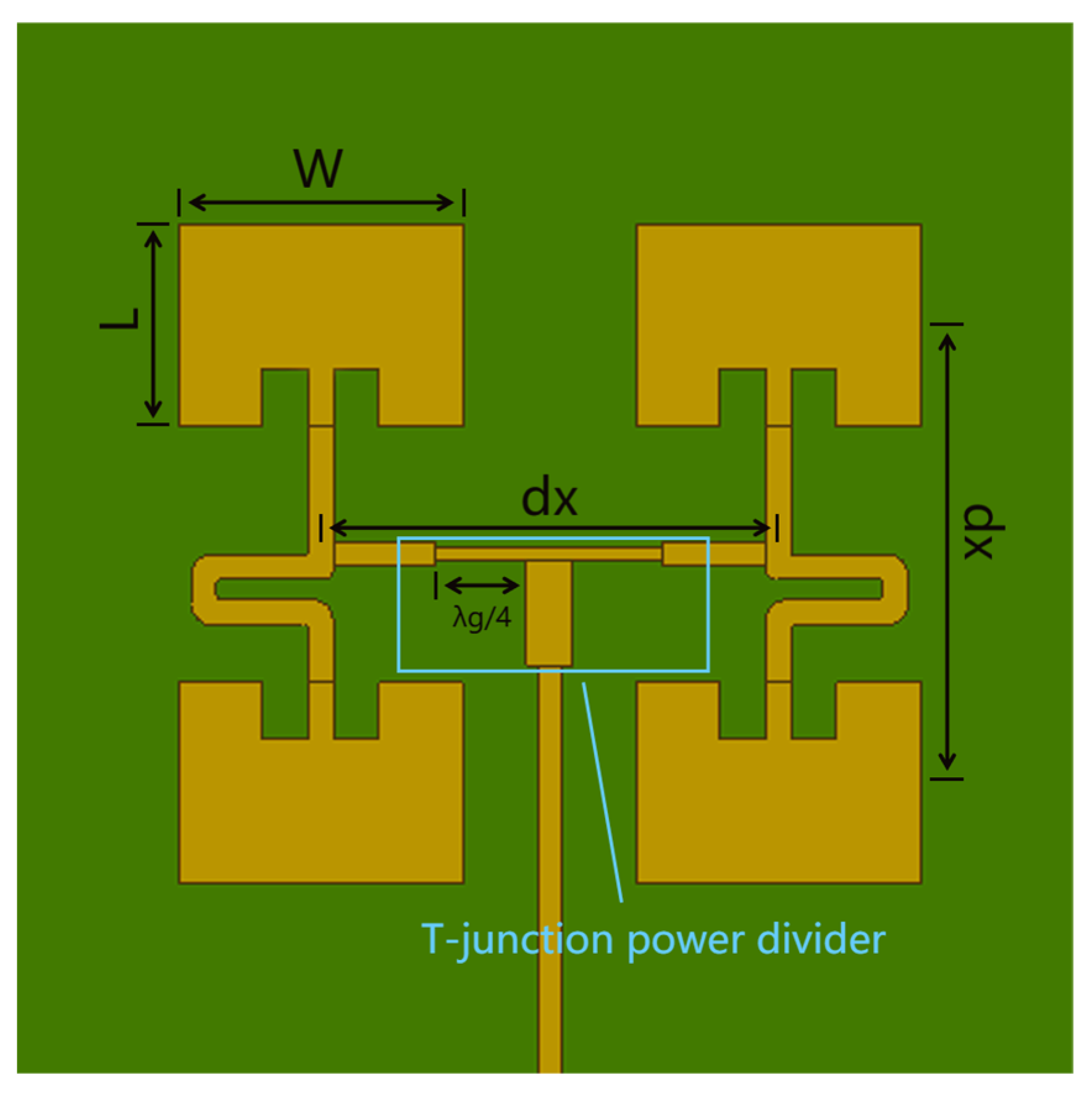
The feeding network incorporates quarter-wavelength impedance-matching transmission lines that are strategically integrated with T-junction power dividers, as shown in
Figure 3. This configuration forms an optimized architecture that ensures the impedance continuity between radiating elements and transmission paths. The hybrid design systematically addresses multi-stage impedance transformation requirements while maintaining signal integrity across all array branches.
Element spacing critically governs radiation integrity. Excessive spacing (d
x) leads to grating lobe formation, which diverts parasitic radiative flux and consequently degrades gain performance. For microstrip array architectures, the optimal spacing parameter d
x must adhere to the dimensional constraints specified in Equation (5). This approach enhances the principal lobe while effectively suppressing parasitic radiation modes.
Optimal element spacing achieves a critical balance, with the empirically established value of effectively suppressing the grating lobes along undesired angular trajectories (θ) while maximizing radiative efficiency. This strategic spatial distribution preserves the integrity of the principal lobe, delivering peak gain-directivity performance by rigorously avoiding energy diffractive dispersal mechanisms.
The final optimized feeding network for the 2 × 2 microstrip patch array is methodically illustrated in
Figure 3. Compared with conventional series-fed configurations, the implementation of a T-junction power divider not only ensures the equitable distribution of input power across each radiating element, but also effectively circumvents phase shift accumulation along the transmission path. Furthermore, the incorporated phase-matching topology within the divider architecture substantially suppresses the return loss while maintaining exceptional amplitude coherence throughout the operating bandwidth.
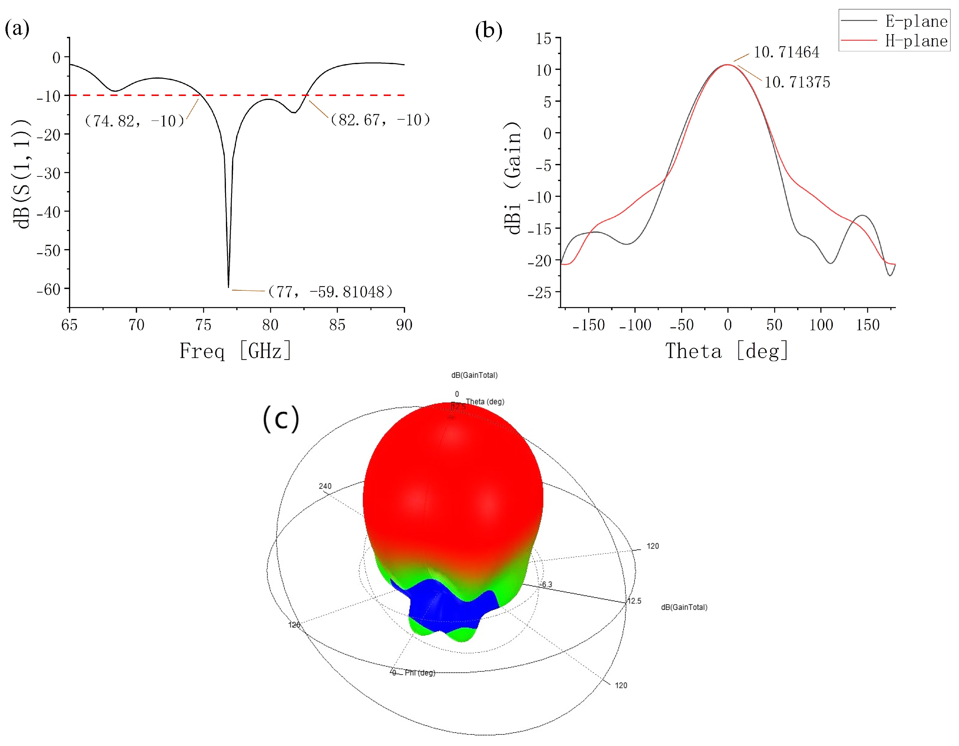
Figure 4 presents the simulation results, which include the reflection coefficient S11, the gain radiation patterns for both the E-plane and H-plane, and the 3D gain pattern of the antenna array. The antenna exhibits a return loss below −10 dB across the 74.82–82.67 GHz spectrum, achieving an absolute bandwidth of 7.85 GHz (the relative bandwidth up to 10.2%). The half-power beamwidths for the E-plane and H-plane range between 63° and 65°, demonstrating excellent directional performance. Notably, the implementation of the antenna array yields significant improvements in bandwidth, gain, and directivity, delivering robust technical performance that fully complies with the design specifications.
3. Fabrication and Results
The performance evaluation of the antenna array employs a ground-signal-ground (GSG) probe configuration for precise characterization, with the detailed probe topology illustrated in
Figure 5a. This specialized contact interface ensures accurate radiofrequency measurements by maintaining controlled impedance through an optimized ground plane arrangement and minimized parasitic coupling. The GSG configuration integrates radiators with extended interconnecting feedlines inserted into precisely dimensioned contact pads, designed to meet the 100 μm pitch probe tip requirements. Critical ground plane geometries were parametrically optimized through rigorous electromagnetic simulations, resulting in final pad dimensions of
LP = 500 μm and
WP = 800 μm, complemented by positioning slots measuring
LC = 200 μm and
WC = 150 μm for optimal impedance matching.
Figure 5a presents the complete antenna array architecture incorporating these measurement-optimized interface structures.
The microstrip antenna array is fabricated on a 4-inch fused silica glass wafer with a thickness of 200 μm, featuring antenna patterns formed from 500 nm thick gold metallization. Through photolithographic patterning and chemical development processes, the antenna geometry is precisely transferred from the photomask to the wafer. Subsequently, vacuum metallization coupled with precision lift-off techniques transforms the photolithographic patterns into functional metallic antenna structures. The crystalline substrate then undergoes precisely controlled dicing processes to yield individual antenna arrays ready for implementation or characterization. Upon the completion of the exquisitely coordinated fabrication procedures delineated above, the antenna array configuration exhibited in
Figure 5 was definitively ascertained. This monolayer antenna architecture eliminates multi-layer alignment complexities, enabling complete fabrication through a single processing sequence. Moreover, the compact 2 × 2 antenna array configuration permits the batch production of multiple units per wafer, substantially reducing the processing intricacy and manufacturing costs through enhanced productivity.
In S-parameter and radiation characteristic measurements, antennas require the precise alignment and calibration of RF probes via GSG probe stations to ensure measurement accuracy. Initial probe adjustment involves leveling the tips perpendicular to the substrate plane. Subsequently, the probes are connected to SOLT calibration standards containing short, open, and 50 Ω loads, with a detailed characterization of the reflection coefficients (S11/S22) and transmission coefficients (S21/S12) across operational frequencies. Measurement protocols mandate the avoidance of physical contact with the test structure during measurement to prevent probe misalignment. This systematic calibration methodology ensures proper system calibration, minimizing loss and ensuring reliable measurement results.
The microstrip patch antenna array was characterized through S-parameter measurements using a ground-signal-ground (GSG) probe-connected vector network analyzer (VNA). The probing system incorporated Newertest’s 110 GHz millimeter-wave test probes, while the VNA system comprised a Keysight PNA-L series instrument with a fundamental measurement range of 50 GHz, extended to 110 GHz via broadband frequency extension modules. The measured
S11 reflection characteristics are presented in
Figure 6a.
The radiation characteristics were measured using a millimeter-wave anechoic chamber and an automated antenna testing platform integrating an antenna under test positioning control and antenna instrumentation processing.
Figure 6b provides a comparative analysis of the simulated versus measured antenna gain patterns.
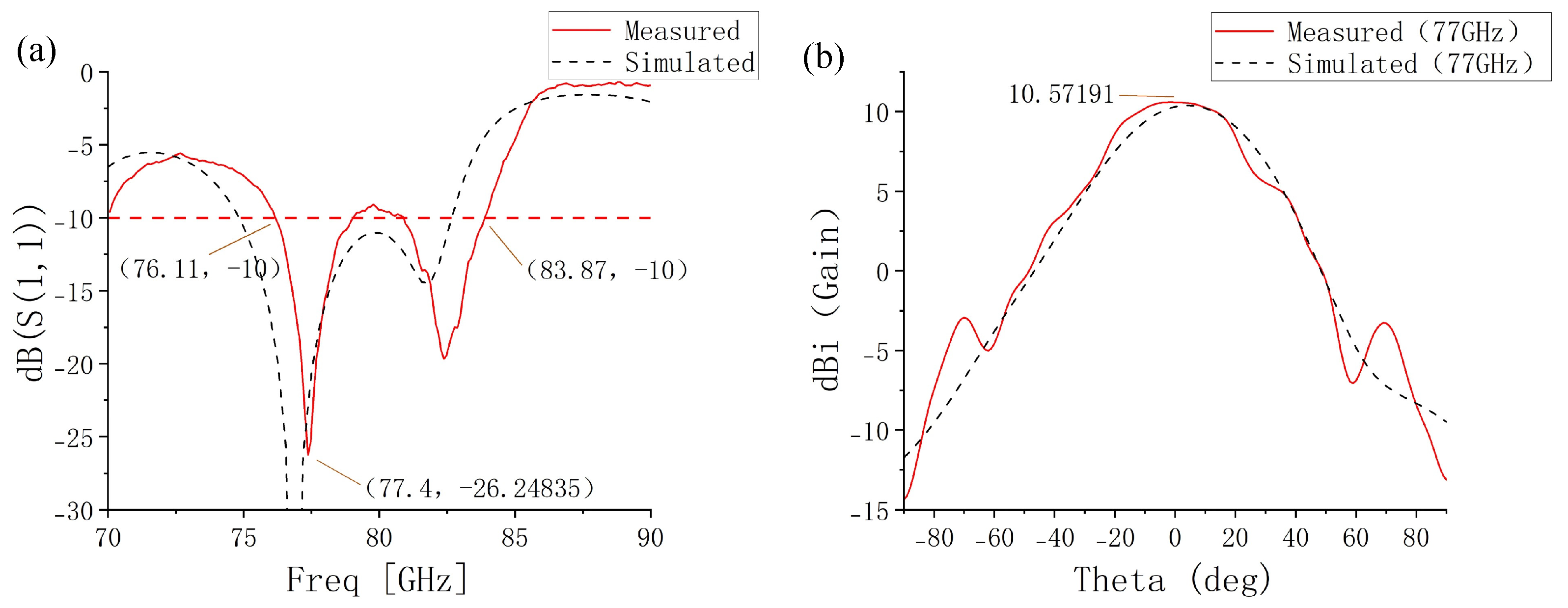
The measured results of the microstrip antenna array, as presented in
Figure 6, show excellent agreement with the simulation predictions across both return loss and radiation characteristics. The fabricated antenna demonstrates an impedance bandwidth from 76.11 to 83.87 GHz (10.1% relative bandwidth), completely encompassing the designed 77 GHz operational frequency while achieving a peak gain of 10.57 dBi. The measured radiation patterns exhibit remarkable consistency with simulations, particularly in main beam alignment, side lobe levels, and beamwidth characteristics, confirming the design’s effectiveness in meeting the target performance specifications.
Table 3 provides a comprehensive comparative analysis of the performance characteristics of this work against recent W-band microstrip antenna designs. The proposed configuration demonstrates distinct advantages, including a notably broad operational bandwidth, and exceptional gain retention achieved with a minimal 2 × 2 element configuration. This streamlined architecture not only meets millimeter-wave radar requirements with enhanced structural simplicity but also facilitates cost-effective mass production through simplified manufacturing processes, making it highly suitable for on-chip integration in advanced millimeter-wave systems.
4. Conclusions
This work successfully demonstrates a compact W-band 2 × 2 on-chip microstrip antenna array fabricated on a glass substrate, showcasing significant advantages in bandwidth, gain, and manufacturability. The glass substrate, with its ultra-low dielectric loss and stable permittivity, enables the array to achieve a 10.1% fractional bandwidth (76.11–83.87 GHz) and a peak gain of 10.57 dBi, while maintaining consistent radiation patterns with beamwidths of 63–65°. The measured performance aligns closely with 3D-EM simulation results, validating the design’s effectiveness. Furthermore, the use of the glass substrate enhances structural simplicity, reduces fabrication costs, and supports the compatibility with standard semiconductor processes, making it an ideal platform for millimeter-wave and terahertz antenna applications. These attributes position the proposed antenna array as a highly suitable solution for next-generation systems, including automotive radar and 6G communication frontends.


