1. Introduction
Modern electrical grids—particularly smart grids and digital substations—require high-speed and reliable data exchange mechanisms for efficient protection, monitoring, and control. The IEC 61850 standard has been widely adopted as a foundational framework for substation automation, offering interoperable communication protocols among Intelligent Electronic Devices (IEDs) and associated equipment within substations [
1]. Central to IEC 61850 is the Sampled Measured Values (SMVs) service, which replaces traditional analogue connections by streaming digitised current and voltage samples over Ethernet-based process buses. Although this transition significantly improves interoperability and reduces wiring complexity, it introduces stringent real-time requirements. Typical software-based implementations of SMVs subscribers running on general-purpose processors frequently struggle to meet the demanding latency and jitter constraints posed by modern substation operations, often handling thousands of SMVs packets per second per IED [
2,
3]. These limitations create significant risks in terms of packet loss and increased latency, impairing timely protective responses.
Recent studies emphasise the necessity of hardware-accelerated solutions to overcome such bottlenecks. In [
4], the importance of meeting stringent timing requirements in digital substation communications is highlighted, as defined by IEC 62351 standards [
5], through FPGA-based implementations. They demonstrated that FPGAs provide effective solutions for performing real-time cryptographic functions like AES-GCM encryption at wire-speed, significantly reducing latency and enhancing communication security for IEC 61850 layer-2 messages such as SMVs and GOOSE. Similarly, in [
6] it is shown how FPGA-based systems efficiently manage Quality of Service (QoS) in real-time communication scenarios through orthogonal frequency division multiplexing (OFDM), demonstrating FPGA’s capability to deliver deterministic and high-throughput performance even under demanding real-time communication conditions. Moreover, FPGA-based architectures inherently offer parallel processing advantages, as exemplified in [
7], who validated the efficacy of FPGA-integrated system-on-chip (SoC) solutions in healthcare applications, achieving significant reductions in power consumption and latency compared to traditional computing platforms.
Drawing on these insights, this paper proposes an FPGA-accelerated SMVs subscriber implemented within a Multi-Processor System-on-Chip (MPSoC) platform. By delegating SMVs data decoding to dedicated FPGA logic, the proposed architecture achieves deterministic, parallel processing of incoming SMVs streams, substantially reducing packet handling delays. The FPGA-based subscriber efficiently parses and updates incoming SMVs streams at wire-speed, thereby bypassing the overhead introduced by conventional software stacks and enhancing real-time communication reliability. Concurrently, processor cores within the MPSoC remain fully available for executing higher-level supervisory and control functions [
8], thus ensuring both high-speed operation and functional flexibility.
The proposed design fully exploits the inherent parallelism offered by FPGA technology, facilitating simultaneous processing of multiple SMVs streams. This architecture thereby significantly enhances scalability, making it ideally suited for large-scale digital substation deployments with growing numbers of interconnected sensors and controllers. Moreover, implementing the subscriber within reconfigurable logic ensures adaptability and compliance with evolving IEC standards, including future editions of IEC 61850 and IEC 61869-9 [
9]. Through experimental validation, the proposed FPGA-based subscriber demonstrates notable improvements in end-to-end latency and data throughput, clearly illustrating its capability to address the stringent real-time requirements posed by contemporary smart grid infrastructure and substations. The main contributions of this work are:
FPGA-Based SMVs Subscriber Architecture: A novel MPSoC-based architecture for SMVs subscription is presented, in which an on-chip FPGA fabric performs high-speed SMVs frame parsing and data extraction. This hardware design eliminates software processing bottlenecks, achieving deterministic low-latency delivery of sampled values.
Addressing Latency and Scalability Limits: The proposed solution is shown to meet the stringent real-time requirements of protective relaying, even as the number of SMVs streams increases. By exploiting parallel processing, it overcomes the latency and throughput limitations of conventional software-based subscribers, improving scalability in large substations.
Performance Evaluation and Benchmarking: A prototype implementation on a AMD/Xilinx Zynq 7000 Series MPSoC is evaluated against traditional CPU-based processing. Empirical results demonstrate significant reduction in processing delay (per-sample latency) and improved reliability under heavy traffic. The FPGA subscriber consistently outperforms a software reference in both speed and capacity, highlighting its effectiveness for high-speed substation communication networks.
Finally, this paper provides a detailed analysis of the proposed architecture and its performance.
Section 2 reviews substation networking concepts and the IEC 61850 SMVs protocol format and rates.
Section 3 approaches a brief data date discussion based on interface limitations and protocol specifications.
Section 4 describes the FPGA-based subscriber design and integration within the MPSoC, including key components and timing considerations.
Section 5 presents experimental results comparing the hardware-accelerated approach to a software implementation, demonstrating how the FPGA solution addresses latency and interoperability challenges.
Section 6 offers conclusions and outlines future work.
2. Substation Networks
The International Electrotechnical Commission’s (IEC) 61850 standard delineates comprehensive and integrated data models for the automation and control systems of electric substations. Spearheaded by IEEE in collaboration with Technical Committee Number 57 Working Group 10 (TC57 WG10) specializing in Ethernet-based communication, this standard enjoys extensive recognition and adoption within the industry. It proffers an all-encompassing data modelling methodology and an abstraction strategy that serves to standardize data structure formats across equipment procured from various vendors [
10]. One key feature presented in the IEC 61850 requirements consists in a novel approach to allow all sensors measurements to be available simultaneously to all controllers within a control network by introducing the process bus concept. Hence, IEC 61850 could be adopted for distributed and decentralized control schemes. The main purpose of this standard is to achieve the Plug-and-Play concept for all the networks used for SA.
The standard defines 3 levels of SA network hierarchies that are used to separate the data traffic between the substation measurement, control, and protection hardware, as presented in
Figure 1.
Each of the hierarchy levels represented above are distinguishing between 10 distinct data categories as follows:
(1) (2)—Data used for the protection functions of the substation IEDs;
(3) (8) (9)—Data transferred through specific SA architecture definition;
(4)—Raw measured data;
(5) (6)—Data used to control the IEDs specific functions;
(7)—Data used to monitor the overall substation behaviour;
(10)—Data used for substation centralized control.
To properly interface with the substation’s raw measured data IEDs, two principal concepts must be taken into account: the Process Bus—as delineated in Part 7 [
11] of the IEC 61850 standard—and the SMVs mapping—defined in Part 9.2 [
12]. The latter portion of Part 9.2 specifies a configurable dataset, which is designed to be transmitted on a multicast basis from a single publisher to multiple subscribers. This approach is particularly significant as it offers an elegant and concise solution for acquiring the sampled values from numerous IEDs within the substation, all interconnected via a single physical communication link.
In a hardware-accelerated environment, where rapid encoding or decoding is imperative, three main aspects must be considered: the Hardware Interface, Ethernet Communication, and the SMVs Protocol itself.
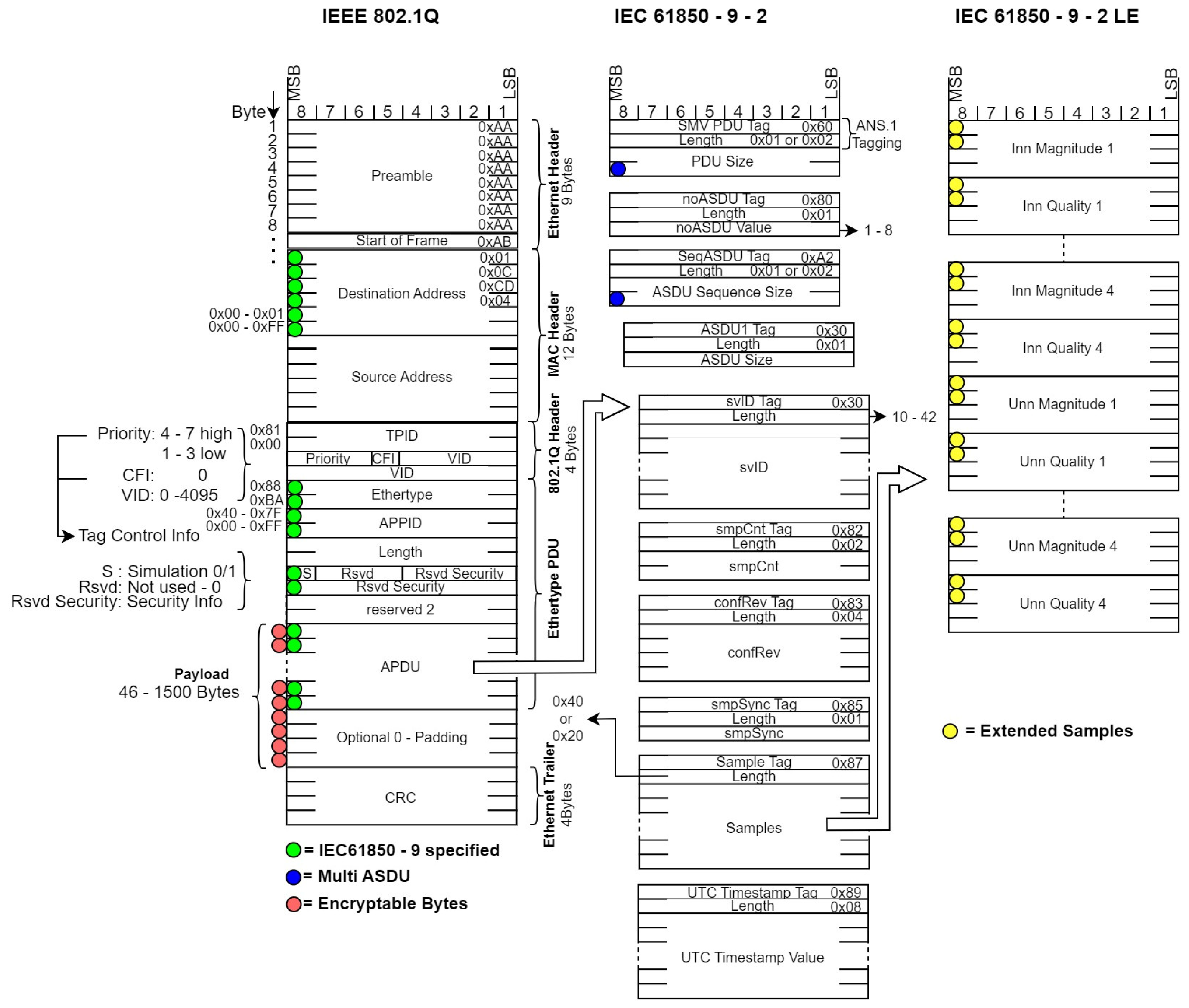
Figure 2 presents a simplified abstraction of the dataset. In this illustration, the specifications prescribed by the standard are clearly segregated from the implementation guidelines, thereby providing a dual perspective on both the theoretical framework and its practical realisation.
The Hardware Interface is defined by IEEE 802.3 standard set [
13], according to the maximum data transmission speed. IEC61850 adopts these definitions along with the specifications regarding the virtual network tagging, but in this case the tag is used to define additional parameters of the packet, for example the decoding priority. The Ethertype field defined by IEEE 802 [
14] for the SMVs network packets and the IEC61850 specifications are treated exactly as an application data for the packet. The SMVs samples are encapsulated into Application Specific Data Units (ASDU) which are contained within Application Payload Data Unit (APDU). Each field of an APDU is marked using Abstract Syntax Notation One (ASN.1) standard to separate the contents of the packet and provide the field length information required to decode the contents in the form of Tag.Length.Value encapsulation of payload data [
15]. Because the IEC61850-9 provides only the Ethernet encapsulation and signalling rules for the application payload data, the encoding of the sampled can vary from one implementation to another, still leaving the device vendors with notable interoperability challenges. The 9-2-LE implementation guidelines are defined to reduce the interoperability problems by defining each ASDU as containing a fixed number of 8 samples, but this is not a requirement as different implementations can accommodate other quantities of data with different encodings.
According to the defined data set, the devices which are sending the sampled data values are called publishers, and the ones which receive the sampled data are called subscribers. An SMVs subscriber has to check every SMVs-tagged packet from the process bus network and only decode a specific set of applications, as defined in its configuration. The decoding delay has some strict margins according to the IEEE C37.118.2 standards [
16]. Even though most traditional implementations of the decoding algorithms are not struggling to meet the time limits, the situation changes when more complex algorithms are running on the same microprocessor which performs the decoding and synchronization. Having a hardware accelerated solution using MPSOCs is offering a deterministic and much lower data latency, while allowing the microprocessor to be loaded with many more complex algorithms, as the decoding will be performed independently of its activity. Also, using this type of architecture, the vendors can develop devices which can easily be updated at the hardware level to keep up with the new revisions of the standard, while also keeping a partial or a full backwards compatibility between the IEDs.
3. Data Rates Overview
Depending on the interface’s performances, the system architecture is chosen to meet the requirements. The data speed for a process bus can start from 100 Mbps in the case of protection measurements and go up to 10 Gbps for the case of sampled value data. The subscriber core is aimed at two possible architectures to support the above-mentioned speed rates:
X8: designed to efficiently use resources to decode, order and process data for speeds up to 1Gbps;
X32: designed to support higher data rates, but at the cost of more resources to implement the data decoding and ordering.
In
Table 1, the maximum data speed is calculated for each of the considered architecture options. The numbers after “X” are indicating the number of bits used for the width of the main data feeding bus from the interface CDC. The X32 architecture implementation for system slower than 1 Gbps is using too many of the FPGA’s resources, and that is where the X8 architecture can take advantage of the lower resource requirement to saturate the data feeding rate and represents a starting point for the developed prototype.
The development of the subscriber core was focused on the internal data decoding and filtering, leaving out the design of a specific MAC module. This decision was made because there are already plenty of transceiver options of the market, with standardized interfaces for microcontrollers and microprocessors.
The process bus speed is capped by the Ethernet physical implementation. There are a few common variations which require different transceivers with specific MAC implementation, each of them requiring a different internal module to decode the received data. In
Table 2, three standardized implementations of the network connection are presented, along with the maximum achievable data speed and Commercial-Off-The-Shelf (COTS) available MAC interfaces.
The SMVs protocol has a base structure defined by the standard, while allowing a few commonly used variations. The maximum number of streams in a process bus is determined by the SMVs specific implementation and the performance of the network. The effective speed of receiving the measured samples is impacted by the overhead data of the transactions, which can have different values according to the implementation approaches. The main variations of the transaction size can be assigned to the following factors:
SMVs data definition can be of either 2B (16 bits) or 4B (32 bits) per sampled value and quality field, corresponding to a Sample Tag length of 32 or 64 bytes;
ASDU definition must have an svID field size between 10 and 42 bytes, leading to different overhead data size of the transactions;
ASDU Sequence definition can significantly impact the data transfer efficiency as it can contain more than a single ASDU.
In
Table 3, values of the samples per second which can be received according to different implementation approaches w.r.t. the transaction fields presented above are presented. For the svID field, a value of 30 bytes was considered, resulting in an added overhead data of 60 bytes per ASDU which must be received to identify each set of sampled values. As for the Ethernet overhead, if we are not considering any padding data then we will have 39 bytes of overhead data, added with the inter-packet gap (IPG) delay which is specific to the network speed according to the standards [
17].
The formula used to calculate the ASDUs per second is presented below:
The Sequence Overhead parameter represents the extra data bytes required to send a sequence of ASDUs in the same data packet, and it is equal to 9 bytes. In a similar manner, ASDU OH represents the number of data bytes used by each ASDU to encapsulate the data samples, and it is considered to be 60 bytes. As specified by the standard implementation guidelines, an ASDU will contain 8 samples, resulting in the final value of the samples per second. The data throughput calculated in the right-most column represents the actual percentage of the bandwidth used to transmit sampled measured data. It can be observed that packing multiple ASDUs in a sequence can have a considerable impact of the data transmission efficiency, as it has a major impact on reducing the overhead data required.
4. Results
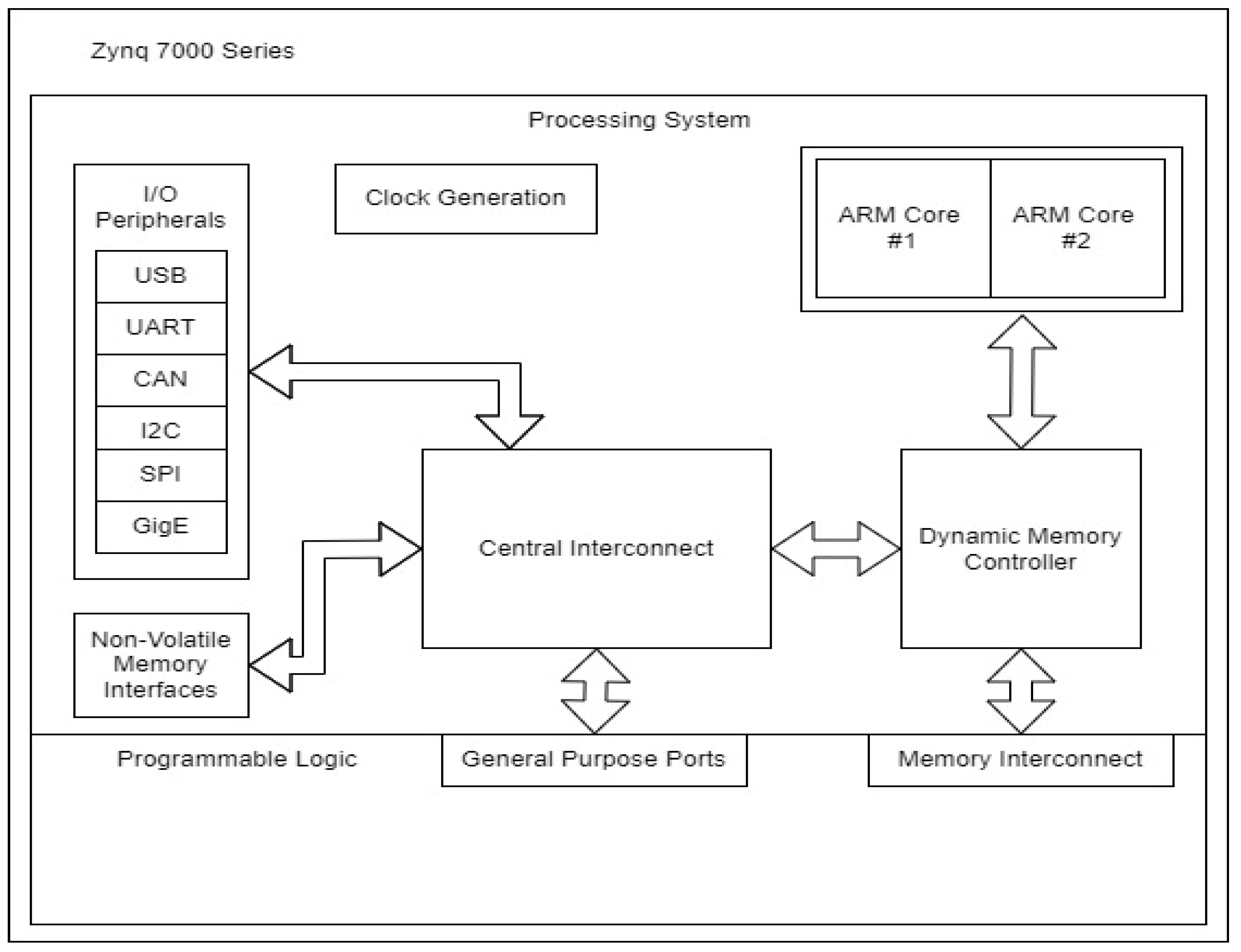
The chosen hardware platform for developing the SMVs Subscriber prototype is Zynq 7000, as presented in the
Figure 3. The architecture representation is a simplified version compared to the datasheet [
18], and it highlights the key components of the system. This SoC family integrates the software programmability of an ARM-based microprocessor with the hardware programmability of an FPGA, enabling versatile functions to be implemented in both hardware and software for remarkable performances.
The programmable logic from the figure above is a simplified representation of the FPGA component, which can be used not only for dedicated features implemented at logic circuit level, but also for customized interconnecting solutions for the components inside the chip. One key advantage of the hardware platform is that it allows direct connections between the FPGA component and the microprocessor’s external dynamic memory, resulting in the possibility of high amounts of data transferred between the two, without a dedicated high speed data bus.
The high-level architecture of the subscriber prototype is presented in the
Figure 4. The main components required to decode and filter the SMVs data are defined at the FPGA level. In this manner, the main features are partially isolated from the microprocessor, requiring only configuration data from the main software. The decoded data is sent to the shared memory controller, and can be accessed by the ARM core using the system virtual memory definition. Both decoded data and configuration data are flowing between the microprocessor, FPGA and dynamic memory using standardized AXI interfaces. This allows not only a high performance level of data transfer, but also a very good level of inter-compatibility of the FPGA cores between different similar SoC architectures.
To take advantage of the FPGA parallelization capabilities and deterministic latencies, the design is built as a single pipeline with a loose level of coupling between the modules. This means that each module can process the data and then pass it to the next module, and the next module only needs the data from the previous one to do the same and pass it further. One significant advantage of this approach is the fixed delay required by each module to send the data to the next module in the data flow. The blue lines are used to represent the data traffic handled by AXI interfaces. AXI Lite is used to handle the configuration data between the ARM and the RTL main access point, while AXI Full is used to write the decoded data into the dynamic memory of the system. One data path that needs to be highlighted is the Decoded Data BUS, which holds not only the decoded data, but also parallelized unique metadata for each stream. This information will be a crucial element in future developments because it will facilitate the rapid identification of data streams for the processing blocks and other features. In the data flow figures, we are referring to the above-mentioned metadata as Data ID, as in the current implementation only contains the associated internal ID to replace the high amount of bytes required by the original svID.
The first module of the subscriber architecture is represented by the SMVs Front-End (FE) which encapsulates the main data receiving interface (IF), along with the required modules to cross the received data from the IF clock to the core clock and an Ethernet filter to let only trusted MAC values to pass further in the pipeline. This module accommodates two different clock domains, one for driving the data IF and one for passing the filtered data to the rest of the modules at a much higher speed than it is received at. The main functionality of this modules resides into two finite state machines (FSM) and a data buffering solution to solve the clock domain cross (CDC) problem. When crossing between different clock domains, there is not a universal solution for every situation. In this particular case, the aim is to cross metadata from a slower clock domain to a faster one. To achieve this, a dedicated dual-port memory block (BRAM) was used as a Buffer to write the incoming data from the IF. While the write-dedicated FSM (FSM W block) controls the data write logic, it also checks the packet for a minimum length value, IEC61850 tags and virtual network tagging fields. After the verification is complete and if the IF error flag was not triggered, 1 element of metadata corresponding to each healthy packet is written into an asynchronous first in first out (FIFO) component, which is designed specifically to work with a different clock domains for data writing and reading [
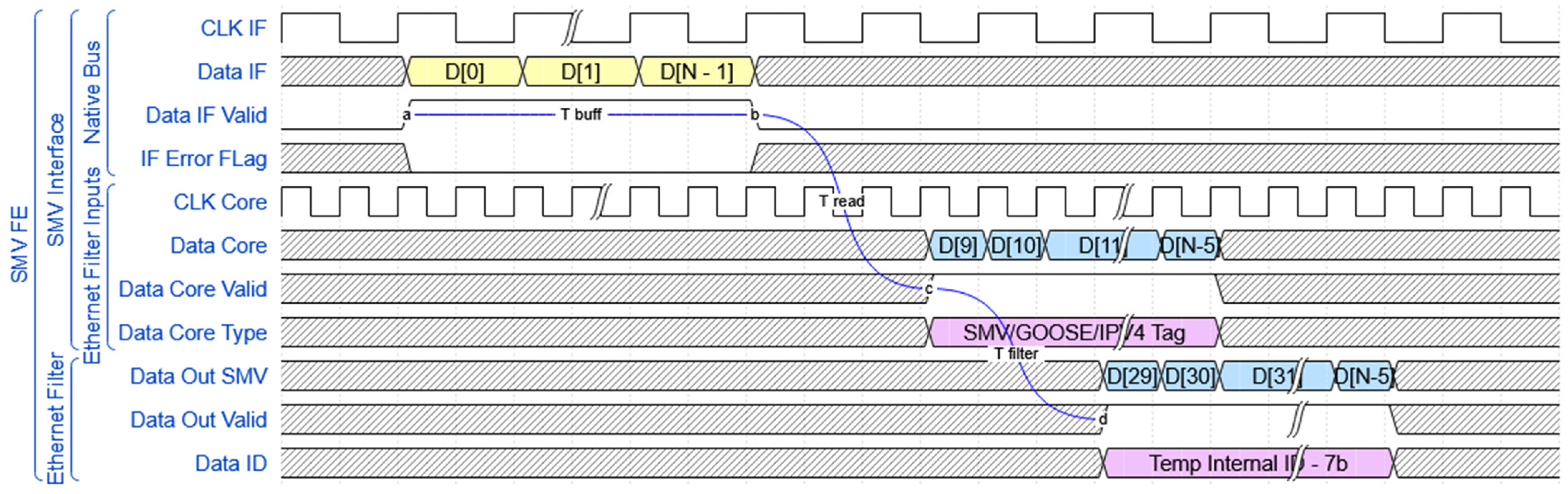
19]. For this, a non-configurable size of 32 elements has been used to compensate the delay caused by smaller packets that can be received, while a larger packet is being read out. The other read-dedicated FSM (FSM R block) has the role to read this metadata as soon as it is available, and use it to get the required information to read the data from the memory block mentioned earlier. When a new metadata element is available on the read clock domain, the buffered data is already stable due to a considerable amount of clock cycles already elapsed. The Buffer has no special rules for crossing the data between the clock domains, as we rely on the stability of the metadata to determine the correct time to read the raw data without the Ethernet header and trailer—13 bytes less. All Buffer modules from the diagram have a non-configurable size of 4096 elements to provide a minimum latency accommodation and take advantage of the entire physical BRAM units, used for implementation. In
Figure 5 can be observed the data entering and exiting the FE module. The figure also presents the data inputs and outputs for the FE module, using a native interface. The different clock domains are labelled as CLK IF—the clock signal used to capture data from the IF, respectively CLK Core—used to analyse the data and drive the rest of the modules. Any module used to drive an Ethernet physical IF can be easily adapted in a manner to connect with the basic native IF, and the inherited error flag can be used to signal any kind of data corruption on the MAC module used. The last component of this module is represented by an Ethernet filter, which checks if the MAC Header is matching with any of the unique values provided in the configuration data, and replaces the Ethernet data up to and including the APPID field. By doing this, the 12 bytes describing the source and destination of the data packet are replaced by a 7 bits unique identifier, making further data identification actions much easier and faster.
This module’s latency is described by three key time intervals:
Tbuff—Buffering delay dependent on the data packet size;
Tread—Constant readout delay which is not affected by the packet size;
Tfilter—Constant filtering delay which is not affected by the packet size.
Using only 7 bits to represent every valid possible MAC Header leads to a restriction of 2^7 − 1 possible values, as 7’h00 value will be treated as not configured. As presented in several studies for performance evaluation [
20], due to signal integrity consideration, a wired process bus can support up to 32–40 different devices for 1 GbE interfaces, even less for 100 Base. The wireless medium is the only one which can support higher values, thus the above chosen value should be representative enough for a prototype model. Using the native IF for the main development process leaves scalability, as it can be adapted to other Ethernet standards in the future.
The 2nd module from the pipeline is represented by the SMVs filter. The main function of this module is to check whether the SMVs identifier (svID) matches any of the configured values. This block is very similar with the Ethernet Filter block, but enhanced to support much higher element size and search space. The module is driven by a main read-dedicated FSM, which controls the ID Decoder and reads the samples from the Buffer block if a match is performed. The Register Space is used to provide the svID values used by the ID Decoder. These values are written/read in the configuration process and they are not latency sensitive. IEC61850-9-2 defines a value between 10 and 42 bytes for this field and it represents the main value used in data abstraction, which is one of the strongest points of the standard. In
Figure 6, the data flow of the SMVs filter is presented.
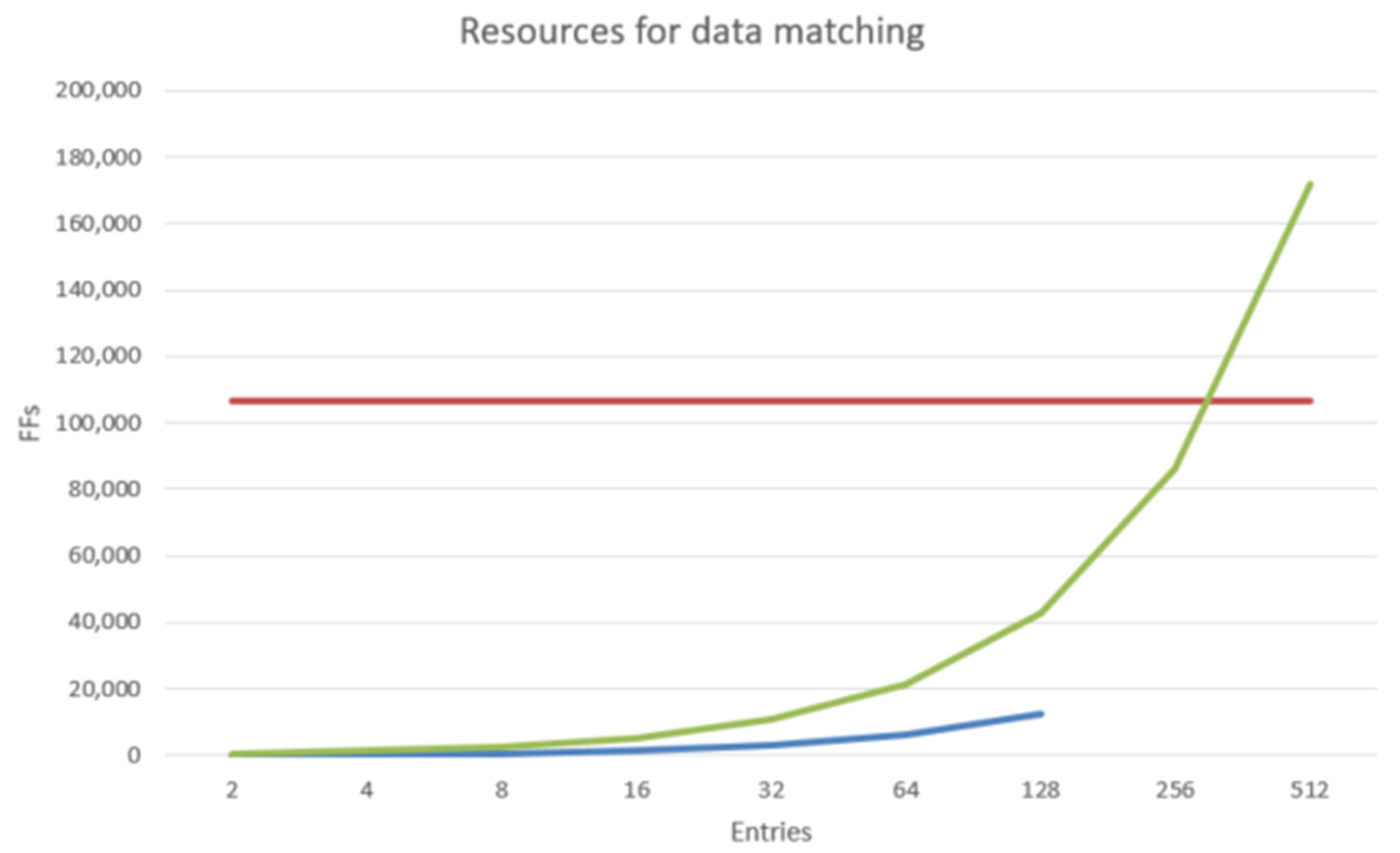
In a similar manner as the Ethernet filter component, this module replaces the lengthy svID and the rest of the SMVs payload overhead with an extension of 9 bits, forming the full internal ID. The challenge of storing the configured values into the FPGA ramps up even more for this module. Each value of the replaced data is after all configured into a register space, which rises the questions of the resources used to store the configuration data. In the figure below is presented the theoretical requirement for Flip-Flops (FFs) elements to store each bit of data from the configuration interface, so the modules can use it to compare the incoming data streams.
The blue line from
Figure 7 represents the theoretical FF resource requirement to store a number of Ethernet MAC headers as a read-write register space, and the green line represents the resource requirement for SMVs identifiers. The red line represents the total FPGA resources available, which according to the datasheet [
18] is 106,400 FF units. One of the key targets of the developed prototype is the ability to filter up to 512 distinct application identifiers. Even though the optimization process leads to slightly lower resource requirements than the theoretical presented values, it is very clear that a conventional approach of defining an independent register for each configuration data byte cannot meet the requirements. Also, even for a low number of data entries the design would use a lot of resources and the congestion level will ramp up. To address this problem, a complex binary search algorithm found in an abandoned patent [
21] and was adapted for both SMVs FE and SMVs Filter modules. The main notable advantage of the algorithm is the possibility of storing the configuration data into memory blocks, while having a deterministic matching delay for the incoming data. One important requirement of the algorithm is that the configuration data needs to be sorted by the ARM core, before being sent to the FPGA register space. The sorting process for data entries of this size is very demanding in terms of processing power, but this is not an issue as the configuration is only performed at the initialization process. Once the configuration data is written into the FPGA register space, the matching process can be performed at a very fast rate, without corner cases and bottlenecks in the data stream. Having a binary search implementation reduces the above-mentioned resource required to store the configuration data to 0 FFs at the cost of using a few memory blocks, depending on the maximum number of data entries. The main delay of this module is represented in the
Figure 6 as T
filter, which is a constant delay.
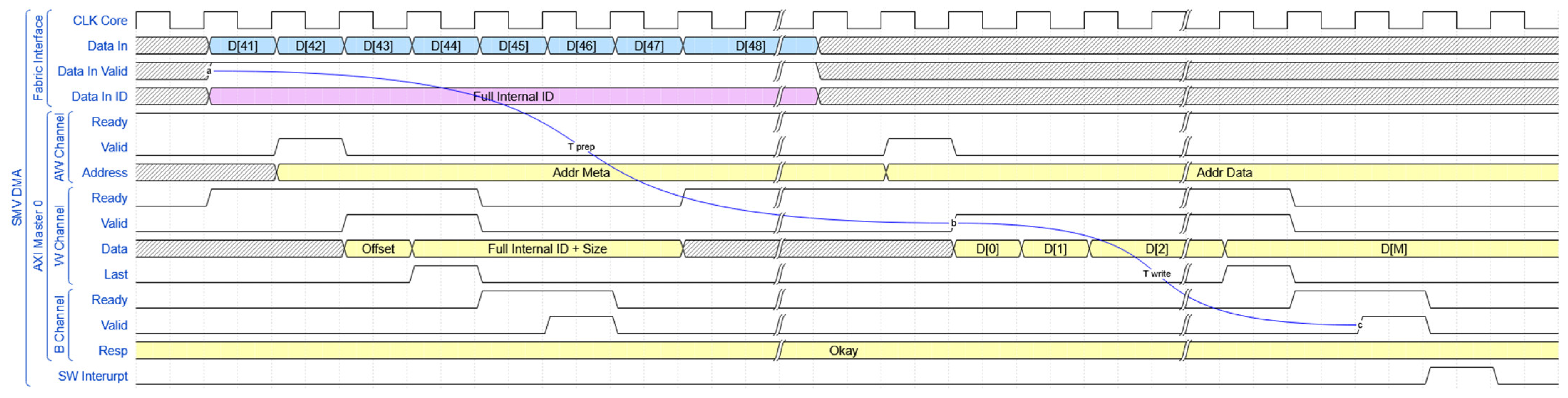
The last module from the data pipeline is represented by the SMVs Dynamic Memory Access (DMA) which performs the basic function of writing the filtered data stream into the system’s external dynamic memory. This block is composed by a basic AXI Write Engine (AXI WE block), along with a Buffer to store the data until the memory is available. As the data arrives at this module in a single byte bus, the first action performed is to write into the memory the metadata of the filtered stream. This consists of the full internal ID, stream size and the address offset where it will be written. The next step is to packetize the data stream into 4-byte elements and send it to the memory using AXI4- Full protocol. In
Figure 8 is presented the simplified data flow of the module.
After the data is successfully written into the dynamic memory, a processor interrupt signal is generated by the Interrupt Generator (IG block) and used to halt the system CPU when the data can safely be read from the memory. The latency of this module is dependent on 2 memory transactions and the size of the data stream. Because the memory controller operates at a much higher frequency than the FPGA modules, even if we are saturating the protocol speed we will not saturate the controller’s capabilities. For 100Mbps and 1Gbps process bus speeds, this module can handle the memory transactions of the filtered data without ever saturating the AXI bus, because a lot of the incoming data is discarded in the pipeline even for the valid streams.
The last component of the FPGA design is represented by the Stripped AXI Register Access (SARA) Hub, which provides the ARM core access to the FPGA register map. The only reason of not using a standard AXI module is for conserving resources due to the large number of registers and also make the configuration signals easy to follow on the simulation diagrams. This block is represented by a straight-forward protocol translator (AXI 2 SARA block) which synchronizes the AXI interface with the internal SARA interface. After the translation, a Splitter block is used to provide an interface for each of the subordinated modules.
5. Discussion
A Zynq 7020 SoC (MYiR Electronics Limited, Shenzhen, China) has been chosen as the target architecture for testing the prototype implementation. This model belongs to AMD Zynq 7000 series and represents a cost effective and high performance-per-watt solution for smart applications with high data rate requirement.
In
Figure 9, the main block design which was used to accommodate the SMVs subscriber component along with the main processing system and vendor-provided miscellaneous blocks required for synchronization and interconnection are presented. These blocks are an out-of-the-box solution which in most of the cases are working properly if the developer has no other problems with the connected components.
Due to architecture limitation, the maximum achievable stable clock speed for the core section is 200 MHz. On newer architectures, the same RTL components can be implemented at higher clock speeds, due to newer programmable logic technology.
The SMVs_Subscriber block encapsulates the entire behaviour presented in the previous section. This implementation version focuses only on the decoding functionality of the prototype. Because the main data path was built as a single pipeline with multiple stages, we are not forced to wait for the data decoding algorithm to perform other actions on the data stream. The design is built in such manner that future functionalities can easily be added to the main features. Having access to and internal data bus, where data is already decoded, offers many integration possibilities for specific optimized features, such as time of arrival checking or data accumulation-based algorithms.
A data generator module has been used for preliminary testing and data rate analysis. This offers a possibility to easily configure test packet sequences, with known delays and configurable content down to OSI layer 2. In terms of delay analysis, the pipeline-based architecture of the SMVs subscriber ensures minimal processing latency, even under worst-case conditions with high data throughput. The combination of hardware-accelerated decoding and efficient memory management contributes to the system’s ability to maintain real-time performance, a crucial requirement for IEC 61850-compliant applications. Preliminary tests using custom data packets and Wireshark captures [
22] confirmed the correct operation of the decoding algorithm, reinforcing the system’s reliability in handling high-speed SMVs streams. The processing system is used to read and write the configuration registers of the prototype, and also to readout the decoded data from the DDR memory. The same control interface is shared with the data generator, as it’s only needed for configuration actions and it’s not latency critical. When the decoded data is written into the DDR memory, an interrupt signal is used by the programmable logic to flag the data validity to the processing system.
As the prototype is still quite far away from field testing, this approach offers a good decoding delay reference, along with the possibility of easily debugging the encountered post-implementation problems. In
Table 4 are presented the resource requirements obtained after implementing different configuration variants of the SMVs Subscriber component. The same configurations are also used for the delay analysis.
To further validate the implementation, multiple configuration scenarios were tested to assess the system’s ability to handle increasing data loads while maintaining stable performance. The results indicate that even in the most resource-intensive configurations, the FPGA utilization remains within acceptable limits, ensuring sufficient headroom for future expansions and additional processing functionalities. Given the relatively low consumption of LUTs and flip-flops, the design demonstrates strong scalability, allowing integration into more complex substation automation systems without significant overhead.
The programmable logic resources required for the different implementations are under 5% of the total resources available on the FPGA, except for the Block RAM which can go to almost 8%. In most cases when data storing algorithms are required, the Block RAM can represent a bottleneck resource. In the presented case, a high number of IDs must be stored to decode the incoming data. This level of utilization proves that we can accommodate the SMVs subscriber prototype in a larger design with many other components. There is still room for optimization as some of the approaches used at different parts of the design are not in their final version. The addition of an Ethernet MII interface to the current state of the prototype is not expected to exceed more than a few hundreds of LUTs and FFs, thus not having a significant impact on the presented resource requirement values.
One notable limitation of re-programmable architectures is represented by the maximum clock frequency which can be used to drive the Programmable Logic. In this particular case, the implemented RTL can be driven with a clock frequency value up to 200 MHz, without having stability problems. The development was focused on avoiding platform-specific RTL components, so it can be easily synthesized on newer vendor-similar devices.
The total data latency of the subscriber prototype is represented as the total delay from the first data byte received by the SMVs FE, until the triggering of the processor interrupt flag. To better understand these values, we need to expand each delay component presented in the modules data flow, as follows:
SMVs FE (running on both clocks)
- ○
Tbuff = N * (CLK IF period)
- ○
Tread = 2 * (CLK Core period)
- ○
Tfilter = (2 * (8/8) * log2(MAC Count) + 3) * (CLK Core period)
SMVs Filter (running only on CLK Core)
- ○
Tfilter = 2 * (64/8) * log2(svID Count) + 3
SMVs DMA (running only on CLK Core)
- ○
Tprep = Taddress + Twrite + Trespond + Tdata = 12 + 2 + 12 + (N − 44 − 12 − 2 − 12)
- ○
Twrite = Taddress + Twrite + Trespond = 12 + ((N − 44)/4) + 12
For sending the address and receiving the response on AXI, 10 extra clock cycles delay were added to account for a worst-case scenario. In
Table 5, the absolute values for the above-mentioned delays are presented, using different parameters for the packet definitions. To keep a consistent comparison, the delays are calculated for one of the most inefficient SMVs packing, using only one application per packet and the maximum defined size for the application identifier (42 bytes). Another 22 extra bytes were added to each element of the memory space to preserve uniformity and unique svID information for future work. When considering the case of multiple application data sets per packet, the total delay until the data set is written into the memory is considerably smaller after the first set, as the FPGA subscriber must process a single Ethernet overhead for multiple application data sets. The clock periods for these calculations were considered as 8 ns for the interface clock—corresponding to a frequency of 125 MHz, and respectively 5 ns for the core clock—corresponding to a frequency of 200 MHz. This was the maximum achievable core clock value, due to Programmable Logic limitations and the achieved optimization level. The most latency sensitive data streams for SMVs Subscribers imposed by IEC61850 are defined as Class P SMVs streams, which must have a total end to end latency of under 3 ms. As can be seen in the previously presented table, the obtained latency scores are around 0.001% of the maximum allowed processing delay.
It is important to take into account that the data has still a few steps missing from the decoding process. The values presented are accounted for native IF implementation, but the variation with the different types of IFs are only at the scale of a few CLK Core cycles. As a comparison reference with traditional implementations, we can consider a recent open-source approach [
23] which debates the data decoding delays of a full power computer processor and another embedded microprocessor. There is a scarcity of information regarding the exact latencies of traditional software solutions, as each of them differ in capabilities and decoding algorithms. Even in the presented reference, we can only find the latency values for the protocol basic identification of key fields, without any information of the delay required to identify the svIDs from the incoming packets. As our prototype is using a 64-byte element definition, we can compare the implemented HW algorithm’s latency with the latency required by different platforms to search a 64-byte element in a table with 256/512 unique elements, as presented in
Table 6. Note that the values presented are corresponding only for the supported features of the SMVs Filter block. There is room for optimization even in software, but it is very difficult to compete with the values obtained from customized hardware.
In comparison, the design implemented at the FPGA level has a single source of semi-deterministic latency variations—the dynamic memory. In the calculations presented in
Table 5, the memory latencies were considered with a very pessimistic margin which requires intensive continuous usage to be reached. Even if we are decoding data from a 1 Gbps network, the resulting traffic on the AXI bus is not nearly enough to be considered a continuous usage of the dynamic memory.
6. Conclusions
This paper has demonstrated that implementing SMVs decoding directly within FPGA logic of an MPSoC platform yields deterministic, microsecond-scale latency superior to conventional software-based solutions, making it particularly suitable for stringent real-time substation protection and control applications. Through rigorous testing, the architecture has proven capable of reliably handling multiple concurrent SMVs streams at throughputs up to 10 Gbps, while utilising minimal FPGA resources −8% RAM, thus leaving ample capacity for further development.
The adoption of reconfigurable FPGA technology also ensures flexibility and compatibility with evolving standards such as future editions of IEC 61850 and IEC 61869-9, allowing hardware updates without complete replacement, which significantly reduces lifecycle costs and extends equipment usability. Empirical validation has confirmed substantial reductions in processing latency compared to software-based implementations, resulting in improved synchronisation accuracy, enhanced real-time protection decision-making, and increased power-grid reliability.
Further research will aim to optimise hardware resource utilisation, refine on-chip memory management, and introduce a dedicated Ethernet MII interface for seamless integration with existing commercial transceivers. These developments will facilitate the transition from prototype towards practical deployment, addressing the emerging requirements of modern smart-grid communication infrastructures.


 ,
, 


