Review

Bulk-Driven CMOS Differential Stages for Ultra-Low-Voltage Ultra-Low-Power Operational Transconductance Amplifiers: A Comparative Analysis

DIEEI (Dipartimento di Ingegneria Elettrica Elettronica e Informatica), University of Catania, 95125 Catania, Italy
*
Author to whom correspondence should be addressed.
Electronics 2025, 14(10), 2085; https://doi.org/10.3390/electronics14102085
Submission received: 15 April 2025 / Revised: 14 May 2025 / Accepted: 20 May 2025 / Published: 21 May 2025
(This article belongs to the Special Issue Advanced CMOS Technologies and Applications)

Abstract

:
Energy-efficient integrated circuits require scaled-down supply voltages, posing challenges for analog design, particularly for operational transconductance amplifiers (OTAs) essential in high-accuracy CMOS feedback systems. Below 1 V, gate-driven OTAs are limited in common-mode input range and minimum supply voltage. This work investigates CMOS Bulk-Driven (BD) sub-threshold techniques as an efficient alternative for ultra-low voltage (ULV) and ultra-low power (ULP) designs. Although BD overcomes MOS threshold voltage limitations, historical challenges like lower transconductance, latch-up, and layout complexity hindered its use. Recent advancements in CMOS processes and the need for ULP solutions have revived industrial interest in BD. Through theoretical analysis and computer simulations, we explore BD topologies for ULP OTA input stages, classifying them as tailed/tail-less and class A/AB, evaluating their effectiveness for robust analog design, while offering valuable insights for circuit designers.

1. Introduction

The relentless pursuit of energy efficiency forces integrated circuits (ICs) to operate with ever-decreasing supply voltages. However, this trend poses a significant challenge for analog design, particularly for OTAs, which are the workhorse circuits in many CMOS applications. Indeed, traditional gate-driven OTAs, often relying on the ubiquitous Long-Tailed Source-Coupled Pair (LTSCP) input stage, face limitations in maintaining a full-scale input range and operating effectively with low supply voltages due to inherent design constraints, especially concerning common-mode input range [1].
Low-frequency ULV and ULP analog circuits find usage in many applications, such as wearable devices, Internet of Things (IoT) sensors, wireless sensor networks, medical implantable devices, remote sensing, energy harvested systems, automotive, etc. [2,3,4,5,6,7]. In this framework, several design techniques are available in standard CMOS, including weak inversion operation [8,9,10], inverter-based [11,12,13,14] and fully digital approaches [15,16,17,18]. Furthermore, research extends to non-silicon technologies like carbon nanotube field-effect transistors (CNTFETs) [19,20].
An alternative to the CMOS gate-driven design approach is the body-driven, or bulk-driven, BD, technique which leverages the dependence of the drain current on the bulk-source voltage, avoiding threshold voltage, VT, limitations [21,22,23,24,25]. While digital design has long utilized BD for purposes like leakage current reduction and compensation of VT variations [26,27,28,29,30,31,32,33], its adoption in analog design remains limited. This is partly due to the persisting perception of the body effect as the origin of potential second-order negative effects in analog circuits like latch-up. Moreover, despite early works demonstrating the viability of the BD approach for analog applications thirty years ago [21], several drawbacks have limited its adoption within the constraints of industry standards, including
(a)
Lower transconductance, i.e., the bulk transconductance is lower than the gate counterpart. This translates to lower gain, lower gain-bandwidth product (GBW) and higher noise for a given standby current.
(b)
Access to bulk terminals. Both bulks of p- and n-MOS devices need to be accessible for full BD exploitation. This is not possible in early single-well technology.
(c)
Poor matching and large silicon area. Related to point (b), devices laid out in different wells can have poor matching characteristics and require non-minimum area.
(d)
Maintaining a safe bulk-source biasing voltage. This is to avoid the turn on of the bulk-source p-n junction.
(e)
Poor concomitant BD and subthreshold operation MOS transistor modeling [34]. Performance predictions through simulations may not be accurate under these circumstances.
Despite these drawbacks, the authors believe that CMOS processes and modeling improvements, together with the advance of the design art and the growing demand for ultra-low-voltage, high-swing, low-frequency solutions, make BD solutions nowadays ready for extensive use and general acceptance. In fact, nanoscale technologies make the impact of the analog area requirement in a mixed-signal IC less severe. The common availability of twin-tub CMOS technologies allows both p- and n-MOS bulk terminals to be accessible. Supply voltages lower than 0.5 V make it quite easy to avoid the bulk-source junction to sustain appreciable current and avoid latch up.
To bridge the gap between theoretical research and practical application, demonstrating the viability of BD techniques for robust ULV-ULP operation and high-performance analog circuits [35], this paper investigates BD solutions amenable for the implementation of operational transconductance amplifier’s (OTA) input stages. This first stage plays a critical role in defining the OTA performance as it significantly impacts parameters like common-mode input range, GBW, CMRR (Common-Mode Rejection Ratio), PSRR (Power Supply Rejection Ratio), offset, and noise. Subsequent gain stages, crucial for DC gain, current drive, and output swing, are typically implemented using conventional gate-driven techniques (e.g., common-source configurations), and, for this reason, will not be discussed in this paper. Specifically, here, we analyze BD input stage solutions exploiting MOS transistors in subthreshold regime [10,24,36,37,38,39,40], amenable for nanoampere-range quiescent current operation, particularly relevant for low-frequency ULV and ULP, battery-operated/battery-less applications, where minimizing power consumption is paramount.
The structure of the paper is the following. Section II presents the definition and some background by discussing basic topologies and their working principle. Section III explores improved circuits, deriving the differential transconductance key parameter for each topology. Two categories of topologies are identified: tailed and tail-less. These are further classified based on their operation as Class A or Class AB. Section IV validates the analysis through computer simulations, comparing the performance of different implementations in a reference common CMOS process. Section V concludes the paper by summarizing the findings and outlining future research directions.

2. Definitions and Background

2.1. Definitions

While utilizing the MOS gate as an input terminal for ULV ICs is constrained by the threshold voltage, operating transistors in the subthreshold region can partially mitigate this issue. However, fully overcoming this limitation requires exploiting the MOS bulk as the input terminal, albeit at the cost of reduced transconductance and input impedance, ultimately impacting gain, bandwidth, and noise performance. Eventually, optimal performance for ULV and ULP circuits is achieved by combining bulk-driven and subthreshold-biasing (weak inversion) techniques [41].
The drain current, iD, of an n-channel MOS transistor operated in weak inversion depends on vGS, vBS and vDS and can be expressed as
i D = W L I S e q v G S V T H n k T 1 e q v D S k T
where W/L is the aspect ratio, VTH is the gate to source threshold voltage, IS is the characteristic current given by I S = 2 n μ C O X k T / q 2 , T is the absolute temperature, k is the Boltzmann constant, q is the charge of the electron, μ is the electron mobility, COX is the oxide capacitance per unit area, and n is the slope factor with 1.1 < n < 1.5. In addition, the threshold voltage depends on the bulk-source voltage through the body effect, with γ the body effect coefficient and ϕ F the Fermi potential:
V T H = V T O + γ 2 ϕ F v B S 2 ϕ F
If VDS ≥ 3 kT/q, then the transistor will be in the saturation of the weak inversion region and the iD dependence on vDS can be neglected in (1). In the following designs, we will choose a minimum VDS of 100 mV for all the transistors.
The gate transconductance, gm, is the derivative of iD with respect to vGS at the operating point, hence we obtain
g m = q I D n k T
whereas the bulk transconductance, gmb, defined as the derivative of iD with respect to vBS at the operating point is
g m b = n 1 q I D n k T = n 1 g m
The relatively low ratio of gmb to gm, often between 0.1 and 0.4, highlights the importance of employing suitable techniques to boost the effective bulk transconductance when exploiting the MOSFET body as input terminal. This is particularly important for noise considerations. Indeed, the equivalent input noise voltage spectral density, Sv,in(f), in V2/Hz, for a body-driven MOSFET can be approximated as
S v , i n ( f ) 4 k T γ g m g m b 2 + g m g m b 2 K F W L C o x f + 4 k T R B = 1 n 1 2 4 k T γ g m + K F W L C o x f + 4 k T R B
where k is the Boltzmann constant, T the absolute temperature (in Kelvin), γ the channel thermal noise coefficient (e.g., 2/3 for long channels, higher for short channels), KF the flicker noise coefficient and RB the equivalent series resistance of the body terminal. Both the input-referred thermal noise, scaled by 1 / g m b 2 , and flicker noise, scaled by (gm/gmb)2, tend to be significantly larger than in a comparable gate-driven device. The noise from the body resistance (RB) also adds directly, but it can usually be neglected.

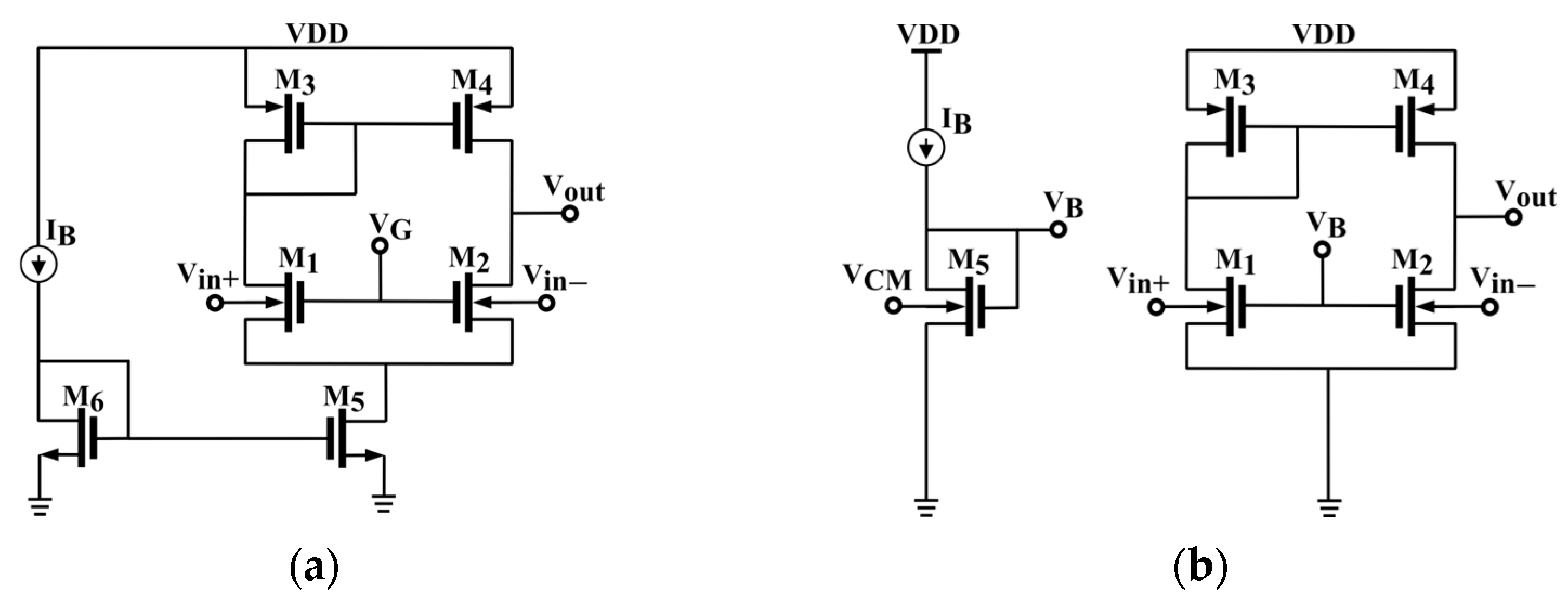
2.2. Basic BD Differential Stage Topologies

This work categorizes the Bulk-Driven OTAs from the literature into two different classes: Tailed and Tail-less solutions. The schematic diagrams of two simple examples are shown in Figure 1, together with the associated current biasing strategy. Importantly, both circuits exhibit a rail-to-rail input common-mode range (0–VDD). The low supply voltage allowed (VDD ≤ 400 mV), effectively prevents significant forward biasing of the parasitic bulk-source junction, thereby minimizing bulk current. Finally, both circuits employ an active load, implemented as a current mirror (M3–M4), to convert the differential input voltage into a single-ended output voltage at the high-impedance output terminal.
The first solution shown in Figure 1a utilizes transistors M1-M2, forming the BD differential pair and M5 as tail current source. Hence, it follows the classical approach, used in gate-driven topologies, with the tail current source that accurately sets the quiescent current of the input stage. Thanks to this, a high CMRR is achieved by reducing the effects of common mode disturbances on the output voltage, but it comes at the expense of the minimum supply voltage that must accommodate 2 VDS + VGS, as can be easily found by following the path from VDD to ground through M3 (that requires one VGS) and M1 and M5 (that require one VDS each). An additional biasing voltage VG is also needed and a discussion on its influence on gmb is found in [34]. Note also that this approach leads to a true differential pair resulting in an equal and opposite current change in the pair (iD1 and iD2) even when single input (e.g., vin+) is applied while the other input is kept at a constant voltage. Finally, the fact that the maximum sinking and sourcing output current is constant and limited to [(W/L)5/(W/L)6]IB dictates that only class A operation is possible. Regarding the small signal differential transconductance, Gmd, and common-mode transconductance, Gmc, we have
G m d = g m b 1 , 2
G m c = ε g m b 1 , 2 1 + 2 g m 1 , 2 + g m b 1 , 2 r d 5
where gmb1 = gmb2 = gmb1,2 was considered, rd5 is the output resistance of M5 and a current transfer 1:(1 + ε) with ε << 1 is assumed in the current mirror from M3 to M4.
Due to supply voltage scaling with technology advancements, BD OTAs are increasingly adopting a tail-less architecture, saving VDS headroom and advantageously enabling class-AB operation. Inherently, however, this approach leads to pseudo-differential operation, which results in a dominant change in one current of the pair (e.g., iD1) when a single input (e.g., vin+) is applied. It must be noted that in conventional gate-driven circuits, the pseudo-differential approach also leads to an ill-defined standby current that depends on the input common-mode level and causes in turn low CMRR. To tackle this problem, techniques like common mode feedback (CMFB), and common mode feedforward (CMFF) can be utilized [41,42,43,44,45,46]. In BD pseudo-differential OTAs, in contrast, this last issue is overcome, as quite good standby current control is achieved. Consider for this purpose the tail-less pseudo-differential BD OTA in Figure 1b. The input BD transistors M1–M2 are biased from their gate via voltage VB that is obtained from diode-connected transistor M5 biased through IB. If the bulk terminal of M5 is kept to the common mode voltage, VCM, of vin+ and vin−, then the common-mode current of the pair is accurately set by the relation: ID1,2 = IB (W/L)1,2/(W/L)5. The supply voltage in this case must accommodate VDS + VGS as can be easily found by following the path from VDD to ground through M3 and M1. The expressions of Gmd and Gmc are
G m d = g m b 1 , 2
G m c = ε g m b 1 , 2
It is seen from (6)–(9) that while the differential transconductances are the same, the common-mode transconductance is adversely higher in (9) due to the absence of the tail current generator.
The equivalent input noise voltage (Sv,in) represents all noise sources within the transconductor referred back to its input (the body terminal). It is calculated by dividing the total output noise current spectral density (Si,out) by the square of Gmd and adding any noise sources directly present at the input.
The topologies in Figure 1 are simple examples, more efficient Tailed and Tail-less solutions are discussed below.

3. High Performance BD Input Stages

In this section, we will discuss three different types of Bulk-Driven input stages. These include tailed input stages, and within the tail-less category, we will distinguish between class-A and class-AB topologies. It is worth noting that unless otherwise specified, the transistor bulk terminals are connected to VDD (for p-channel MOSFETs) and to VSS (for n-channel MOSFETs).

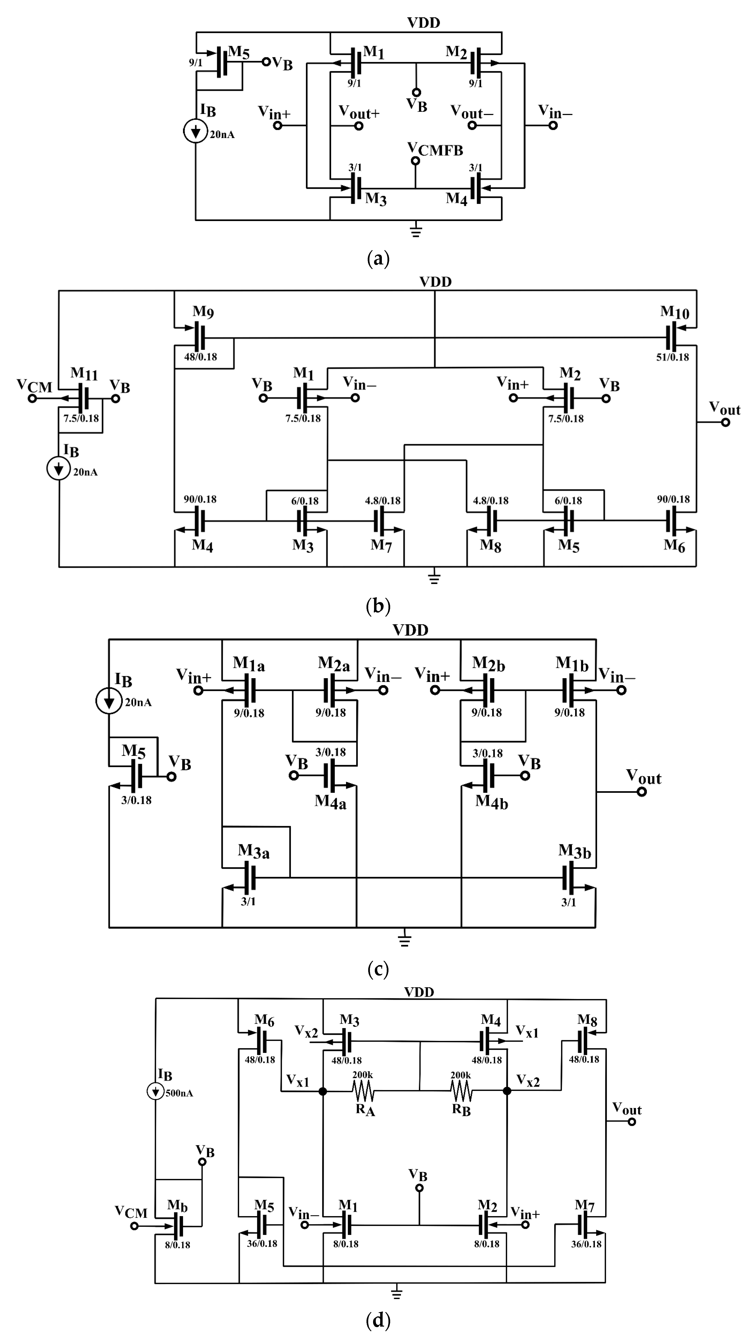
3.1. Tailed Differential Stages

In the category of tailed BD differential stages, we have selected the three exemplifying topologies shown in Figure 2a–c.
Figure 2a depicts the BD OTA proposed in [47]. It utilizes M1 and M2 as the input transistors and M5 as the tail current source. The active load includes the constant current sources M6 and M7, and the self-cascode current mirror made up of composite transistors M3a–M3b and M4a–M4b. This latter (composite) arrangement provides a high output-impedance cascode structure without the need for additional biasing elements. Here, the important requirement is that VGS3b,4b must be lower than VGS3a,4a by at least 3VT to preserve saturation of M3a and M4a and this is obtained via larger aspect ratios for M3b,4b compared to M3a,4a. The minimum supply voltage is 3VDS, as can be seen by following the path from VDD to VSS through M5, M2, and M3a. The full differential transconductance is obtained thanks to the current mirror and is thus equal to gmb1,2.
Figure 2b shows an improved version, originally proposed in [48], that utilizes M1a and M2a as cross-connected active loads degenerating the sources of M1b and M2b, respectively. The solution was then implemented in [49] utilizing the self-cascode current mirror M3a–M4b. The minimum supply voltage is 4VDS. Due to the positive feedback provided, the degeneration boosts the overall transconductance. We can derive the following equation for the equivalent differential transconductance, Gmd, using the small-signal equivalent model depicted in Figure 3:
G m d = ( g m 1 a , 2 a 1 r d 1 a , 2 a ) α g m b 1 a , 2 a α g m 1 a , 2 a 2 g m b 1 , 2 1 B
in which we set gmb1,2 = gmb1a,2a = gmb1b,2b and
α = A 1 B
where denoting as R the resistance seen at drain of M1b,2b, A and B are given by
A = g m b 1 a , 2 a + g m b 1 b , 2 b 1 + R r d 1 b , 2 b g m 1 b , 2 b + g m b 1 b , 2 b + 1 r d 1 b , 2 b 1 + R r d 1 b , 2 b + 1 r d 1 a , 2 a 2 g m b 1 a , 2 a g m 1 b , 2 b
B = g m 1 a , 2 a g m 1 b , 2 b + g m b 1 b , 2 b + 1 r d 1 b , 2 b 1 + R r d 1 b , 2 b + 1 r d 1 a , 2 a
Figure 2. Examples of tailed BD differential stages: (a) [47], (b) [49], and (c) [50].
Electronics 14 02085 g002
It is noteworthy that the positive feedback of the solution, responsible for 1 − B at the denominator in (11), may induce instability for B approaching 1. Therefore, B < 1 must be ensured. Moreover, the inclusion of MOSFET output resistance, rd, improves the accuracy of this equation compared to that given in [48]. This is critical in short-channel technologies, where channel length modulation increases, making gmb no longer negligible relative to 1/rd while gm greater than 1/rd is still reasonable. Furthermore, the varying drain-source voltages necessitate the retention of distinct rd values for M1a,2a and M1b,2b. Finally, for the approximation of (10), we assume gm (and gmb) are equal for M1a,2a and M1b,2b.
It is observed that (10) provides an improved transconductance compared to the original gmb1,2 by approximately a factor of 2/(1 − B). In a well-designed circuit, 1−B can be set within the range of 0.1 to 0.3.
The last solution considered is the one proposed in [50] and illustrated in Figure 2c. It exploits the cross-connected transistors M1b and M2b derived from the two parallel BD pairs M1a,1b, M2a,2b with (W/L)1a,2a = k (W/L)1b,2b. The minimum supply voltage is 2 VDS + VGS1,2 that can equal 300 mV provided that VGS1,2 = 100 mV. Observe that the tail current source is replaced by two flipped voltage followers (FVF) [51] implemented by M1d–M1b and M2d–M2b as variable tail current sources utilizing negative feedback and depending on the amplitude of input signals. Moreover, the cross-connection between the gates and drains of M1b and M2b increases the impedance at their drain terminals, which are in turn connected to the gates of M1d and M2d obtaining an equivalent transconductance boost, as given in (14), where parameters k, m and p, are the standby current ratios as illustrated in the same Figure 2c. Using k = 1, m = 1 and p = 0.25 we obtain a boosting factor of 5. Considering gmb1a,1b = gmb2a,2b = gmb1,2 the overall differential transconductance is given as
G m d = 2 k m 1 + p 1 + k g m b 1 , 2

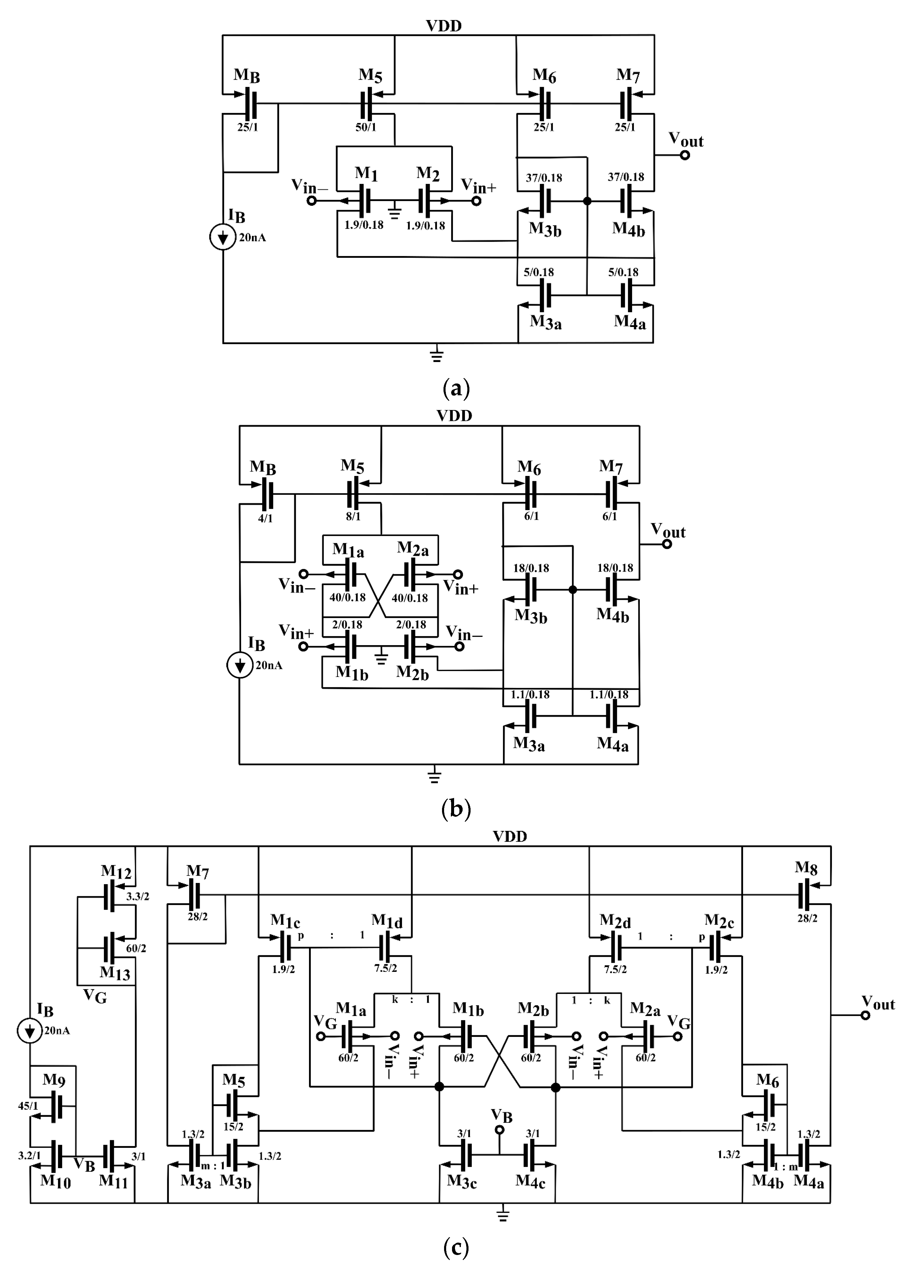
3.2. Tail-Less Class-A Differential Stages

The second category of circuits studied in this review comprises class-A tail-less input stages. Four representative solutions have been selected and are illustrated in Figure 4a–d. Figure 4a, ref. [52], shows the simplest tail-less pseudo-differential input stage which exploits the bulk terminals of both p-channel (M1–M2) and n-channel (M3–M4) transistor couples. M1 and M2 are biased through VB. Due to the fully differential output, the gate voltage of M3 and M4 is driven by a common-mode feedback voltage which also increases CMRR. The common-mode feedback circuit can be simply implemented using two large resistors connected between the gate and drain of M3 and M4, as shown in Figure 4d. More advanced solutions utilize an auxiliary error amplifier, with a specific implementation detailed in reference [52]. The differential transconductance (single-ended) is simply
G m d = g m b 1 , 2 + g m b 3 , 4 2
A simple topology that exploits local positive feedback offered by transistors M7 and M8 to boost the equivalent transconductance is shown in Figure 4b, ref. [53]. In this case, we obtain
G m d = g m 4 , 6 r o 1 1 g m 7 , 8 r o 1 g m b 1 , 2 g m 4 , 6 / g m 3 , 5 1 g m 7 , 8 / g m 3 , 5 g m b 1 , 2
where r o 1 = r d 1 , 2 r d 3 , 5 r d 7 , 8 1 g m 3 , 5 1 g m 3 , 5 .
To avoid Gmd sign changes and stability problems, the ratio of gm7,8/gm3,5 should be kept below 1. This precaution is necessary because Gmd ideally approaches infinity when gm7,8 approaches gm3,5, making the circuit highly sensitive to small variations.
Figure 4c shows a non-tailed BD stage in which the input voltage is applied to the four transistors M1a,b and M2a,b. Transistors M4a,b are constant current sources and M3a,b implement the current mirror for differential to single-ended conversion. An augmented transconductance is obtained by controlling the input transistors M1a and M1b both from their body and gate terminals [54]. For example, considering M1a and M2a, M1a is driven from its bulk by vin+ and also from its gate by a voltage approximately equal to −gmb2a/gm2a vin− (simply consider that gmb2a vin− + gm2avgs = 0 at the drain of M2a). Therefore, the equivalent transconductance of M1a is 2gmb1,2 like the overall equivalent differential transconductance of the circuit. Notably, this configuration achieves true differential operation, thereby surpassing the limitations of pseudo-differential approaches, thanks to its four input transistors.
The circuit in Figure 4d utilizes resistors RA,B for common-mode feedback so that M3 and M4 conduct the same common-mode current of M1 and M2 [55]. Moreover, it exploits local positive feedback implemented by the cross connection of body and drain terminals of M3 and M4 which, together with the current mirror gain provided by M3 to M6 (M4 to M8) improves the equivalent transconductance as
G m d = g m 6 , 8 R A , B r o 1 1 g m b 3 , 4 R A , B r o 1 g m b 1 , 2
where r o 1 = r d 1 , 2 r d 3 , 4 . This solution also ensures true differential operation, as explained in [55].

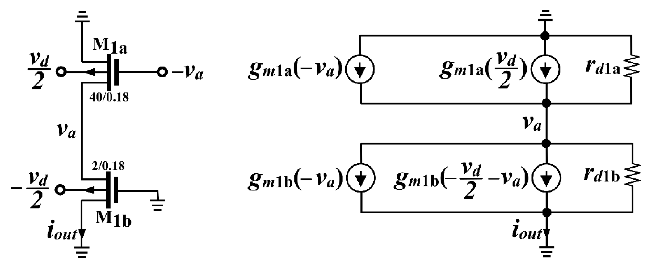
3.3. Tail-Less Class-AB Differential Stages

The preceding tail-less input stages operate in class A, i.e., their maximum output current is limited to the value of the standby current. This characteristic is also inherent to tailed topologies. However, the literature also presents tail-less implementations operating in class AB, capable of delivering output currents significantly exceeding their standby current. The following section explores three such circuits whose schematic diagrams are depicted in Figure 5a–c [56,57,58].
In Figure 5a two self-biasing transconductance cells (M1a–M4a and M1b–M4b) are used as BD tail-less input stages. Transistors M5a,b are added in parallel to M3a and M3b, respectively, to increase controllability of the cells by reducing gm3a,b and to avoid zero current condition. The second stage is made up of common source transistors M6a,b (that are also body-driven to improve current driving capability) and cross-connected transistors M7a,b that mirror the current in M4a,b. The solution offers fully differential operation.
Due to the absence of tail current generators, to improve common-mode rejection the two transconductance cells must be designed symmetrically and well matched with each other to optimize common mode cancelation.
Assuming 1/rd << gm and gm1a,b = gm2a,b = gm4a,b, the positive feedback of the self-biasing input cells leads to a high output impedance [56]. Indeed, the resistance seen at the output node of each transconductance cell, rO1,O2, is expressed by
r O 1 , O 2 1 g m 1 a , b g m 3 a , b
Since gm3a,b < gm1a,b, a positive and finite impedance is achieved. The value of this resistance is electrically controlled by gm3a,b through voltage, VB, at the gate of M5a,5b. Assuming gm6a = gm6b the overall differential transconductance is given by
G m d 2 g m 6 r O 1 , O 2 g m b 1 , 2
In Figure 5b, the tail-less BD differential cell M1-M4 has its standby current set by VB. The output common-mode voltage is set by diode-connected transistors M9–M10, which have zero DC current and thus exhibit very large small-signal resistance around the bias point, similar to RA-B in Figure 4d [55]. These pseudo-resistors establish the common-mode voltage while minimizing the load effect at the output of the first stage. Although they may exhibit nonlinearity under large signal conditions, the output swing remains constrained, as the only node experiencing significant signal swing is the output, and the second stage M5–M8 provides high gain and differential to single conversion. The overall differential transconductance can be expressed as follows:
G m d = g m 6 , 8 r d 1 + g m b 3 , 4 r d g m b 1 , 2
where
r d = r d 1 , 2 r d 3 , 4 r d 9 , 10
The last topology examined in this category shown in Figure 5c utilizes two matched transconductor cells, M1a–M4a and M1b–M4b, similar to those in Figure 5a with the only difference that M4a,4b are diode-connected from body to drain (and not, as usual, from gate to the drain) [58]. The output resistance, ro1,2, of these input cells is equal to
r o 1 , 2 = r d 2 a , 2 b r d 4 a , 4 b 1 g m b 4 a , 4 b
A second transconductance stage, implemented by M5–M8, increases gain and also provides differential to single-ended conversion through BD unitary current mirror M7–M8. The overall differential transconductance is hence given as
G m d 2 g m b 1 , 2 g m 5 , 6 r o 1 , 2
The differential transconductance of all the input stages discussed is summarized for convenience in the second column of Table 1.

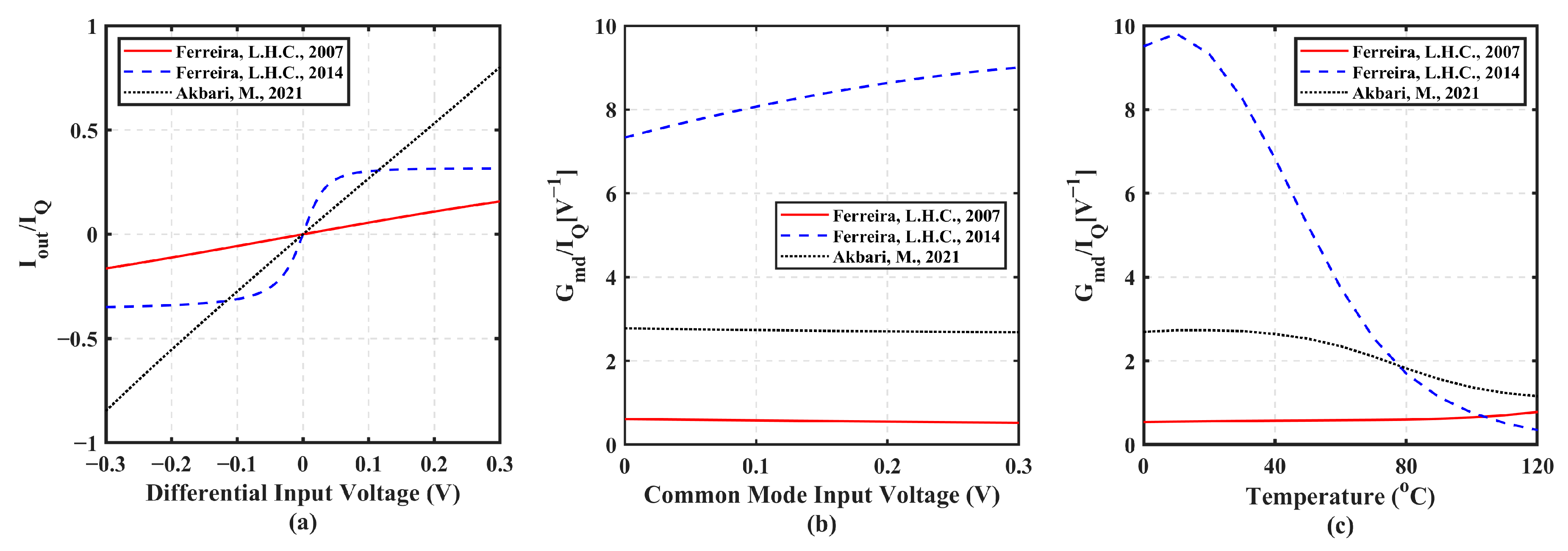
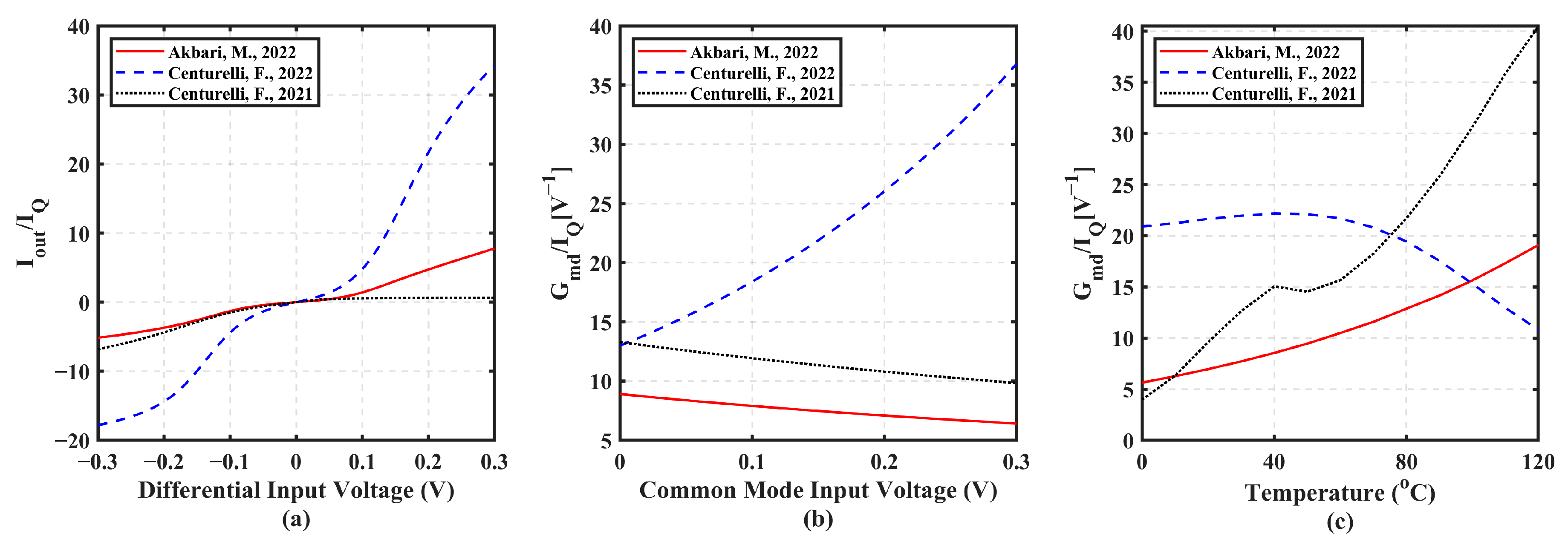
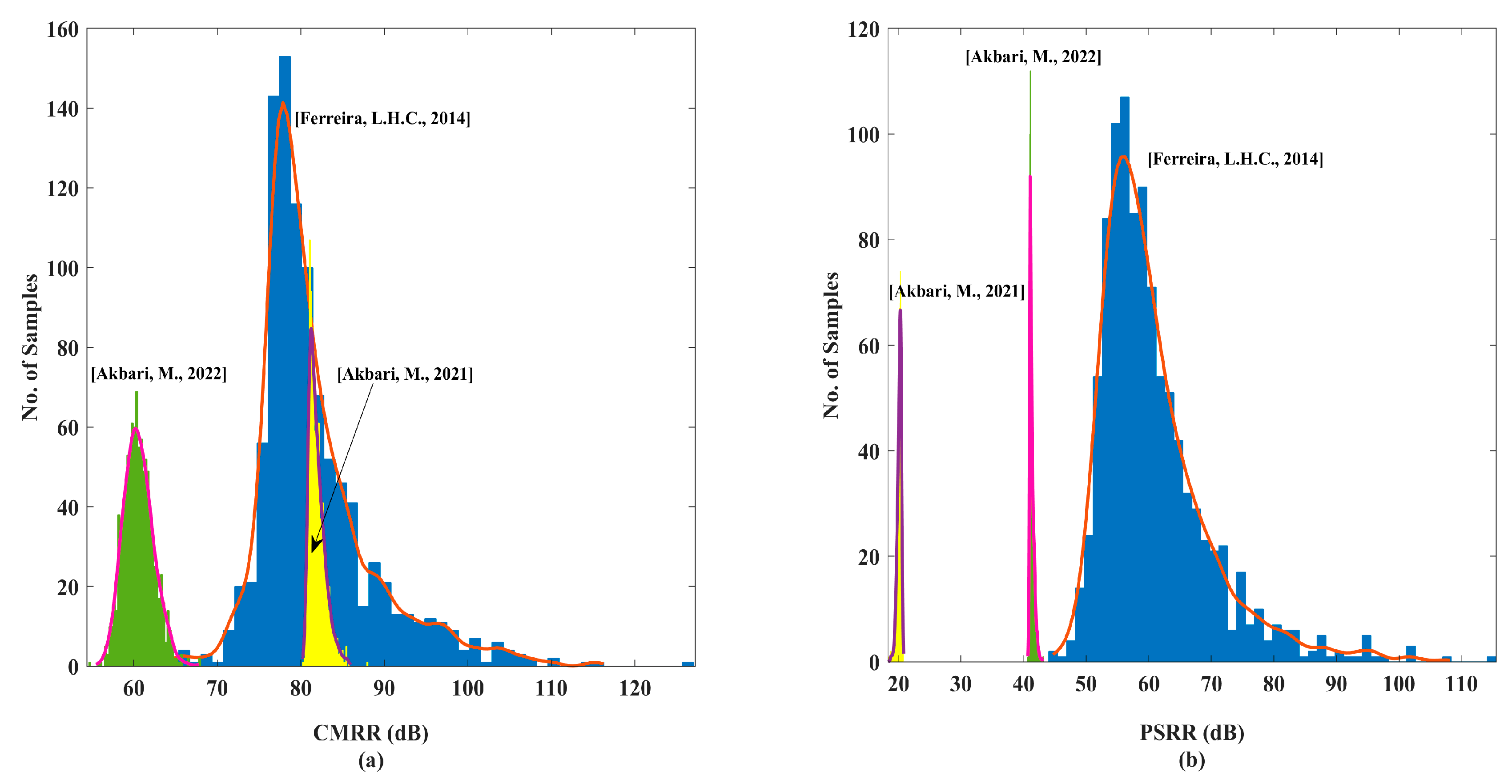
4. Comparison and Discussion

Previously discussed circuits were simulated with Cadence Spectre using the same 65 nm CMOS bulk technology from TSMC to obtain comparative performance parameters. For consistency, a supply voltage (VDD) of 300 mV was used for all circuits, except for the circuit in Figure 2b [49], which required 400 mV. This ensured a MOS drain-source voltage of 100 mV at the operating point for all designs. The transistor dimensions are shown in the schematic diagrams, with labels adjacent to the corresponding transistors. The equivalent differential transconductance (Gmd = iout/vd), common-mode transconductance (Gmcm = iout/vcm), and power-supply transconductance (Gmdd = iout/vdd) were evaluated using the configurations in Figure 6a, Figure 6b and Figure 6c, respectively.
In addition to the discussed Gmd expressions, Table 1 shows the simulated Gmd values (at VCM = VDD/2) and the corresponding calculated values. The latter were derived from approximate equations in Table 1 using the small-signal transconductances and output resistances obtained from the operating point simulation. As evident, there is a very good agreement between the simulated and calculated values, except for [49], which, however, provides a very accurate result if the compete Equations (10), (12) and (13) are used.
The third column of Table 1 provides the W/L, multiplicity factor, and channel type for the input BD transistors. The total standby current is presented in the fourth column, while the fifth column indicates the operating class and tail/tail-less topology. The Gmd/IQ ratio, displayed in the last column, facilitates a more effective comparison of Gmd efficiency relative to current consumption across different solutions. Among the Class A topologies, those with positive feedback exhibit the highest Gmd/IQ ratios [49,53]. Local body-positive feedback in [55] appears less effective. Class AB solutions [57,58] are however the most efficient, with [57] achieving a Gmd/IQ of 21.9 V−1, approximately twice that of [58] (11.7 V−1).
In Figure 7a, Figure 8a, and Figure 9a, the short-circuit output current normalized to the total standby current is plotted as a function of the differential input voltage, for all configurations. VCM = VDD/2 was again set. The curves allow a graphical evaluation of the symmetrical behavior, current drive capability and linearity of the input stages.
In addition, circuit sensitivity to input common mode was assessed by plotting in Figure 7b, Figure 8b and Figure 9b the value of Gmd/IQ as a function of the DC CM input voltage, VCM. Both plot types were obtained using the test bench in Figure 6a.
Results for the tailed configurations are presented in Figure 7. Figure 7a indicates that solutions [47,50] provide excellent current linearity which makes them well-suited for Gm-C filtering applications, where consistent transconductance is crucial for accurate filter response. Topology from [50] shows a steeper linear increase in normalized IOUT compared to [47] as a result of the higher Gmd and the highest current drive capability (80% of the tail current). Moreover, as can be seen from Figure 7b, ref. [50] provides almost ×3 Gmd compared to [47] for the same current consumption. Both topologies are insensitive to input CM voltage value. Topology from [49], which is similar to [47] but uses positive feedback source degeneration, exhibits a notable Gmd boosting. However, this comes at the cost of a reduced linear differential voltage range, with output current saturation occurring near ±100 mV. This limitation is not critical for input stages of high-gain amplifiers, as the virtual short at the inputs effectively mitigates the impact of the reduced linear range. Moreover, as from Figure 7b the transconductance is sensitive to the CM value, exhibiting nearly a ±10% Gmd variation. Therefore, the overall DC gain and the gain-bandwidth product (Gmd/CC, where CC is the frequency compensating capacitance) are functions of the common-mode input. Such variation, although limited, is of course not desirable, as it leads to inconsistent amplifier performance across different operating conditions. Another important trade-off not considered in this paper is that the transconductance boosting by means of partial positive feedback modifies the position of the secondary poles, thus reducing the maximum achievable bandwidth.
Finally, circuit sensitivity to temperature was assessed by plotting in Figure 7c the value of Gmd/IQ as a function of T in °C. VCM = VDD/2 was again set. Circuits in [49] shows the highest sensitivity to temperature with the largest percentual variations over the 0 to 120 °C range considered. Conversely, circuit in [47] shows the minimum variation with temperature.
Figure 8 is related to Tail-less Class A BD solutions. In Figure 8a, only solution [53] achieves a maximum current marginally exceeding IQ, thus can be still considered within Class A topologies. Solutions [52,54,57] display a more consistent and linear slope compared to [54] throughout the differential input voltage range. Nevertheless, [53] demonstrates the highest slope (Gmd) for a narrow input range, approximately ±100 mV. Figure 8b reveals that all configurations are affected by Gmd/IQ variations with common mode, spanning from 25% to 50%. Finally, Figure 8c depicts the value of Gmd/IQ as a function of T. VCM = VDD/2 was again set. Circuit in [53] shows the highest sensitivity to temperature, whereas circuit in [52] shows the minimum one.
Figure 9 is related to the second set of tail-less BD input stages, demonstrating their class AB behavior because Iout/IQ values greater than the unity are achieved. Compared to class A solutions, a high transconductance is also attained. Specifically, the circuit in [58] operates only for negative vd. This limitation arises from the BD current mirror M7–M8, seen in Figure 5c, where increased input current beyond the standby value raises the input voltage, driving M7 out of saturation. The largest Iout/IQ ratio is achieved by [57]. However, Figure 9b shows that all topologies exhibit varying transconductance with VCM, with [57] displaying the most significant variation. Figure 9c shows that [58] has the highest sensitivity to temperature.
Table 2 shows in the third and fourth columns the value of Gmcm and Gmdd obtained again at VCM = VDD/2 (see Figure 6b,c). As expected, the lowest Gmcm values are achieved by Class A topologies [47,49,50]. However, only [47,49] display similarly competitive performance in Gmdd, while [50] provides one of the worst performances. In the same Table 2 we show CMRR (Gmd/Gmcm) and PSRR (Gmd/Gmdd) with their mean and standard deviation from 1000 Monte Carlo simulations at DC. The CMRR and PSRR of all circuits displayed nearly Gaussian behavior, enabling a meaningful use of statistical parameters. The Class A tailed solutions [49,50] yielded the highest CMRR with [50] the smallest standard deviation but it exhibited one of the lowest PSRR. Topology [49] showed also the highest PSRR, but both high CMRR and PSRR values are obtained at the cost of large variations attributed to its positive feedback mechanism. Of the tail-less solutions, [56] demonstrated the superior CMRR and the third best PSRR, while [57], ranking second for PSRR, presented a larger standard deviation. Figure 10a,b show, respectively, the statistical distribution of the magnitude of CMRR and PSRR, for the representative cases [49,50,56]. The larger standard deviation of [50] is apparent.
Corner simulations were also performed, and their results are summarized in Table 3. Comparing the solutions [53] and then [57] show the largest CMRR variation, whereas [50] presents the minimum change. PSRR is generally characterized by a smaller variation.
Finally, noise simulations were carried out. Equivalent input noise voltage for all configurations was evaluated at three frequencies (10 Hz, 100 Hz, and 10 kHz) and is reported in Table 4. The value at 10 kHz represents only white noise, while the values at 10 Hz and 100 Hz also include the flicker noise contribution. Solutions [55,56] exhibit the lowest white noise values, 0.9 μ V / Hz . This is not surprising, as both circuits have the largest standby current consumption, 1.41 mA and 1.0 mA, respectively (from Table 1). For a fairer and more comprehensive comparison of the different topologies, a Figure of Merit (FoM) is introduced, as defined in (24):
F o M = G m d P D C S v , i n , white
It essentially quantifies how efficiently a transconductor provides its primary function (Gmd) for a given amount of power consumed and noise generated. A higher FoM value indicates that the transconductor design achieves a more favorable trade-off. Solution [56] remains the best achieving an FoM value exceeding 31 Hz/V4). This is followed by [49,55]. When considering low-frequency noise, the best performance is achieved by [56,57,58] (in that order), i.e., the class-AB solutions.

5. Conclusions

This work aimed to bridge the gap between theoretical exploration and practical application of body-driven techniques for operational transconductance amplifier input stages, especially within the demanding constraints of ULV and ULP operation. The investigation into subthreshold-based BD input stages, categorized by topology (tailed and tail-less) and operating class (A and AB), has laid the groundwork for their potential in power-sensitive applications. The subsequent data considerations will present a detailed analysis of the simulated performance of these topologies, offering crucial insights into their practical limitations and advantages, thus substantiating the theoretical findings presented herein.
For achieving Gmd efficiency (Gmd/IQ) and current drive, Class AB tail-less solutions [57,58] demonstrate the best performance, with [57] significantly outperforming the others. Among Class A topologies, positive feedback mechanisms in [49,53] lead to the best Gmd/IQ ratios. It is important to observe that unlike all other topologies that operate at 300 mV, ref. [49] requires a higher supply voltage of 400 mV. For achieving high CMRR, Class A tailed solutions [49,50] are the most effective, with [50] offering better robustness against process variations. Reference [56] provides a good balance of CMRR and PSRR on average, with low standard deviation. Also, for applications demanding high linearity, tailed Class A topologies, particularly [47,50], are advantageous. Regarding noise performance, class AB solutions offer the best performance, especially concerning flicker noise. An analysis of frequency performance—an aspect not covered in this paper—would also be relevant, as this performance is often limited in solutions that utilize feedback, especially positive feedback.
These findings underscore the importance of carefully selecting the appropriate body-driven input stage topology based on the specific performance requirements of the target application, considering the inherent trade-offs between gain, linearity, common-mode and power supply rejection, and robustness against process variations.

Author Contributions

Conceptualization, S.P.; methodology, M.O.S. and A.B.; validation, M.O.S. and A.B.; writing—original draft preparation, S.P. and M.O.S.; writing—review and editing, S.P., M.O.S. and A.B. All authors have read and agreed to the published version of the manuscript.

Funding

This work was developed under project SAMOTHRACE (ECS00000022) and funded by the European Union (NextGeneration EU), through the MUR-PNRR.

Data Availability Statement

The original contributions presented in the study are included in the article, further inquiries can be directed to the corresponding author.

Conflicts of Interest

The authors declare no conflicts of interest.

References

  1. Huijsing, J.H.; Linebarger, D. Low-voltage operational amplifier with rail-to-rail input and output ranges. IEEE J. Solid-State Circuits 1985, 20, 1144–1150. [Google Scholar] [CrossRef]
  2. Zhang, F.; Holleman, J.; Otis, B.P. Design of Ultra-Low Power Biopotential Amplifiers for Biosignal Acquisition Applications. IEEE Trans. Biomed. Circuits Syst. 2012, 6, 344–355. [Google Scholar] [CrossRef]
  3. Sharma, P.; Ali, M.S.A.; Misra, S. Ultra-Low Power CMOS Circuit Design for Wireless Sensor Networks. IEEE Sens. J. 2019, 19, 5117–5125. [Google Scholar]
  4. Jha, A.B.R.; Kumar, S.; Gupta, A. Ultra-Low Power CMOS Circuits for Medical Implantable Devices. IEEE Trans. Biomed. Eng. 2020, 67, 2285–2293. [Google Scholar]
  5. Reddy, M.V.M.; Srinivasan, M.L.; Reddy, L. Ultra-Low Power CMOS Energy Harvesting Systems for Remote Sensing. IEEE Trans. Ind. Electron. 2019, 66, 1989–1997. [Google Scholar]
  6. Lee, H.; Choi, S.; Kim, J. Low-Power CMOS Circuits for Battery-Powered Consumer Electronics. IEEE J. Solid-State Circuits 2020, 55, 3112–3123. [Google Scholar]
  7. Shih, C.P.; Huang, S.C.; Tseng, Y.C. Low-Power Design Techniques for Standby and Sleep Modes in CMOS Circuits. IEEE Trans. Very Large Scale Integr. (VLSI) Syst. 2020, 28, 332–343. [Google Scholar]
  8. Vittoz, E.; Fellrath, J. CMOS Analog Integrated Circuits Based on Weak Inversion Operations. IEEE J. Solid-State Circuits 1977, 12, 224–231. [Google Scholar] [CrossRef]
  9. Beloso-Legarra, J.; Grasso, A.D.; Lopez-Martin, A.J.; Palumbo, G.; Pennisi, S. Two-Stage OTA With All Subthreshold MOSFETs and Optimum GBW to DC-Current Ratio. IEEE Trans. Circuits Syst. II Express Br. 2022, 69, 3154–3158. [Google Scholar] [CrossRef]
  10. Grasso, A.D.; Marano, D.; Palumbo, G.; Pennisi, S. Design Methodology of Subthreshold Three-Stage CMOS OTAs Suitable for Ultra-Low-Power Low-Area and High Driving Capability. IEEE Trans. Circuits Syst. Regul. Pap. 2015, 62, 1453–1462. [Google Scholar] [CrossRef]
  11. Nauta, B. A CMOS Transconductance-C Filter Technique for Very High Frequencies. IEEE J. Solid-State Circuits 1992, 27, 142–153. [Google Scholar] [CrossRef]
  12. Figueiredo, M.; Santos-Tavares, R.; Santin, E.; Ferreira, J.; Evans, G.; Goes, J. A Two-Stage Fully Differential Inverter-Based Self-Biased CMOS Amplifier With High Efficiency. IEEE Trans. Circuits Syst. Regul. Pap. 2011, 58, 1591–1603. [Google Scholar] [CrossRef]
  13. Rodovalho, L.H.; Aiello, O.; Rodrigues, C.R. Ultra-Low-Voltage Inverter-Based Operational Transconductance Amplifiers with Voltage Gain Enhancement by Improved Composite Transistors. Electronics 2020, 9, 1410. [Google Scholar] [CrossRef]
  14. Centurelli, F.; Giustolisi, G.; Pennisi, S.; Scotti, G. A Biasing Approach to Design Ultra-Low-Power Standard-Cell-Based Analog Building Blocks for Nanometer SoCs. IEEE Access 2022, 10, 25892–25900. [Google Scholar] [CrossRef]
  15. Crovetti, P.S. A Digital-Based Analog Differential Circuit. IEEE Trans. Circuits Syst. Regul. Pap. 2013, 60, 3107–3116. [Google Scholar] [CrossRef]
  16. Toledo, P.; Crovetti, P.; Aiello, O.; Alioto, M. Fully Digital Rail-to-Rail OTA With Sub-1000-Μm2 Area, 250-mV Minimum Supply, and nW Power at 150-pF Load in 180 Nm. IEEE Solid-State Circuits Lett. 2020, 3, 474–477. [Google Scholar] [CrossRef]
  17. Toledo, P.; Crovetti, P.; Aiello, O.; Alioto, M. Design of Digital OTAs With Operation Down to 0.3 V and nW Power for Direct Harvesting. IEEE Trans. Circuits Syst. Regul. Pap. 2021, 68, 3693–3706. [Google Scholar] [CrossRef]
  18. Privitera, M.; Crovetti, P.S.; Grasso, A.D. A Novel Digital OTA Topology with 66-dB DC Gain and 12.3-kHz Bandwidth. IEEE Trans. Circuits Syst. II Express Briefs 2023, 70, 3988–3992. [Google Scholar] [CrossRef]
  19. Ho, R.; Lau, C.; Hills, G.; Shulaker, M.M. Carbon Nanotube CMOS Analog Circuitry. IEEE Trans. Nanotechnol. 2019, 18, 845–848. [Google Scholar] [CrossRef]
  20. Khaleqi, M.; Jooq, Q.; Behbahani, F.; Moaiyeri, M.H. An ultra-efficient recycling folded cascode OTA based on GAA-CNTFET technology for MEMS/NEMS capacitive readout applications. AEU Int. J. Electron. Commun. 2021, 136, 153773. [Google Scholar] [CrossRef]
  21. Blalock, B.J.; Allen, P.E. A low-voltage bulk-driven MOSFET current mirror for CMOS technology. In Proceedings of the IEEE International Symposium on Circuits and Systems (ISCAS 1995), Seattle, WA, USA, 30 April–3 May 1995; Volume 3, pp. 1972–1975. [Google Scholar]
  22. Guzinski, A.; Bialko, M.; Matheau, J. Body driven differential amplifier for application in continuous-time active-C filter. In Proceedings of the European Conference on Circuit Theory and Design (ECCTD 1987), Paris, France, 1–4 September 1987; pp. 315–319. [Google Scholar]
  23. Jiang, Y.; Raut, R. A low-voltage low-power voltage-to-current transconductor using bulk-driven CMOS transistors. In Proceedings of the 5th International Conference on VLSI and CAD, Seoul, Republic of Korea, 13–15 October 1997; pp. 451–453. [Google Scholar]
  24. Blalock, B.J.; Allen, P.E.; Rincon-Mora, G.A. Designing 1-V opamps using standard digital CMOS technology. IEEE Trans. Circuits Syst. II 1998, 45, 769–780. [Google Scholar]
  25. Grasso, A.D.; Pennisi, S.; Venezia, C. A Survey of Ultra-Low-Power Amplifiers for Internet of Things Nodes. Electronics 2023, 12, 4361. [Google Scholar] [CrossRef]
  26. Narendra, S.; Antoniadis, D.; De, V. Impact of using adaptive body bias to compensate die-to-die Vt variation on within-die Vt variation. In Proceedings of the International Symposium on Low Power Electronics and Design, San Diego, CA, USA, 16–17 August 1999; pp. 229–232. [Google Scholar]
  27. Keshavarzi, A.; Ma, S.; Narendra, S.; Bloechel, B.; Mistry, K.; Ghani, T.; Borkar, S.; De, V. Effectiveness of reverse body bias for leakage control in scaled dual VT CMOS ICS. In Proceedings of the International Symposium on Low Power Electronics and Design, Huntington Beach, CA, USA, 6 August 2001; pp. 207–212. [Google Scholar]
  28. Tschanz, J.W.; Kao, J.T.; Narendra, S.G.; Nair, R.; Antoniadis, D.A.; Chandrakasan, A.P.; De, V. Adaptive body bias for reducing impacts of die-to-die and within-die parameter variations on microprocessor frequency and leakage. IEEE J. Solid-State Circuits 2002, 37, 1396–1402. [Google Scholar] [CrossRef]
  29. Neau, C.; Roy, K. Optimal body bias selection for leakage improvement and process compensation over different technology generations. In Proceedings of the ISLPED ‘03: 2003 International Symposium on Low Power Electronics and Design; Seoul, Korea, 25 August 2003, pp. 116–121.
  30. Roy, K.; Mukhopadhyay, S.; Mahmoodi-Meimand, H. Leakage current mechanisms and leakage reduction techniques in deep submicrometer CMOS circuits. Proc. IEEE 2003, 91, 305–327. [Google Scholar] [CrossRef]
  31. Nomura, M.; Ikenaga, Y.; Takeda, K.; Nakazawa, Y.; Aimoto, Y.; Hagihara, Y. Delay and power monitoring schemes for minimizing power consumption by means of supply and threshold voltage control in active and standby modes. IEEE J. Solid-State Circuits 2006, 41, 805–814. [Google Scholar] [CrossRef]
  32. Kim, K.K.; Kim, Y.B. A novel adaptive design methodology for minimum leakage power considering PVT variations on nanoscale VLSI systems. IEEE Trans. VLSI Syst. 2009, 17, 517–528. [Google Scholar] [CrossRef]
  33. Jeon, H.J.; Kim, Y.B.; Choi, M. Standby leakage power reduction technique for nanoscale CMOS VLSI systems. IEEE Trans. Instrum. Meas. 2010, 59, 1127–1133. [Google Scholar] [CrossRef]
  34. Carrillo, J.M.; Duque-Carrillo, J.F.; Torelli, G. Design considerations on CMOS bulk-driven differential input stages. In Proceedings of the 2012 International Conference on Synthesis, Modeling, Analysis and Simulation Methods and Applications to Circuit Design (SMACD), Seville, Spain, 19–21 September 2012; pp. 85–88. [Google Scholar]
  35. Monsurró, P.; Pennisi, S.; Scotti, G.; Trifiletti, A. Exploiting the Body of MOS Devices for High Performance Analog Design. IEEE Circuits Syst. Mag. 2011, 11, 8–23. [Google Scholar] [CrossRef]
  36. Hollis, T.M.; Comer, D.J.; Comer, D.T. Optimization of MOS Amplifier Performance through Channel Length and Inversion Level Selection. IEEE Trans. Circuits Syst. II Express Briefs 2005, 52, 545–549. [Google Scholar] [CrossRef]
  37. Valero Bernal, M.R.; Celma, S.; Medrano, N.; Calvo, B. An Ultralow-Power Low-Voltage Class-AB Fully Differential OpAmp for Long-Life Autonomous Portable Equipment. IEEE Trans. Circuits Syst. II Express Briefs 2012, 59, 643–647. [Google Scholar] [CrossRef]
  38. Chatterjee, S.; Tsividis, Y.; Kinget, P. 0.5-V Analog Circuit Techniques and Their Application in OTA and Filter Design. IEEE J. Solid-State Circuits 2005, 40, 2373–2387. [Google Scholar] [CrossRef]
  39. Magnelli, L.; Amoroso, F.A.; Crupi, F.; Cappuccino, G.; Iannaccone, G. Design of a 75-nW, 0.5-V Subthreshold Complementary Metal–Oxide–Semiconductor Operational Amplifier. Int. J. Circuit Theory Appl. 2014, 42, 967–977. [Google Scholar] [CrossRef]
  40. Qin, Z.; Tanaka, A.; Takaya, N.; Yoshizawa, H. 0.5-V 70-nW Rail-to-Rail Operational Amplifier Using a Cross-Coupled Output Stage. IEEE Trans. Circuits Syst. II Express Briefs 2016, 63, 1009–1013. [Google Scholar] [CrossRef]
  41. Monsurrò, P.; Pennisi, S.; Scotti, G.; Trifiletti, A. 0.9-V CMOS Cascode Amplifier with Body-driven Gain Boosting. Int. J. Circ. Theor. Appl. 2009, 37, 193–202. [Google Scholar] [CrossRef]
  42. Mohieldin, A.N.; Sanchez-Sinencio, E.; Silva-Martinez, J. A fully balanced pseudo-differential OTA with common-mode feedforward and inherent common-mode feedback detector. IEEE J. Solid-State Circuits 2003, 38, 663–668. [Google Scholar] [CrossRef]
  43. Mohieldin, A.N.; Sanchez-Sinencio, E.; Silva-Martinez, J. Nonlinear effects in pseudo differential OTAs with CMFB. IEEE Trans. Circuits Syst. II Analog Digit. Signal Process. 2003, 50, 762–770. [Google Scholar] [CrossRef]
  44. Bahmani, F.; Sanchez-Sinencio, E. A highly linear pseudo-differential transconductance [CMOS OTA]. In Proceedings of the 30th European Solid-State Circuits Conference, Leuven, Belgium, 23 September 2004; pp. 111–114. [Google Scholar] [CrossRef]
  45. Aamir, S.A.; Wikner, J.J. A 1.2-V pseudo-differential OTA with common-mode feedforward in 65-NM CMOS. In Proceedings of the 2010 17th IEEE International Conference on Electronics, Circuits and Systems, Athens, Greece, 12–15 December 2010; pp. 29–32. [Google Scholar]
  46. Tao, C.; Lei, L.; Chen, Z.; Huang, Y.; Hong, Z. A 29.5 dBm OOB IIP3 TIA Based on a Two-Stage Pseudo-Differential OTA With R-C Compensation and Cascode Negative Resistance. IEEE Access 2023, 11, 24343–24352. [Google Scholar] [CrossRef]
  47. Ferreira, L.H.C.; Pimenta, T.C.; Moreno, R.L. An Ultra-Low-Voltage Ultra-Low-Power CMOS Miller OTA With Rail-to-Rail Input/Output Swing. IEEE Trans. Circuits Syst. II Express Br. 2007, 54, 843–847. [Google Scholar] [CrossRef]
  48. Carrillo, J.M.; Torelli, G.; Duque-Carrillo, J.F. Transconductance enhancement in bulk-driven input stages and its applications. Analog Integr Circ Sig Process 2011, 68, 207–217. [Google Scholar] [CrossRef]
  49. Ferreira, L.H.C.; Sonkusale, S.R. A 60-dB Gain OTA Operating at 0.25-V Power Supply in 130-nm Digital CMOS Process. IEEE Trans. Circuits Syst. I Regul. Pap. 2014, 61, 1609–1617. [Google Scholar] [CrossRef]
  50. Akbari, M.; Hussein, S.M.; Hashim, Y.; Tang, K.T. An Enhanced Input Differential Pair for Low-Voltage Bulk-Driven Amplifiers. IEEE Trans. Very Large Scale Integr. (VLSI) Syst. 2021, 29, 1601–1611. [Google Scholar] [CrossRef]
  51. Carvajal, R.G.; Ramírez-Angulo, J.; Torralba, A.; Galán, J.A.G. The flipped voltage follower: A useful cell for low-voltage low-power circuit design. IEEE Trans. Circuits Syst. I Fundam. Theory Appl. 2005, 52, 1276–1291. [Google Scholar] [CrossRef]
  52. Sala, R.D.; Centurelli, F.; Monsurrò, P.; Scotti, G.; Trifiletti, A. A 0.3V Rail-to-Rail Three-Stage OTA With High DC Gain and Improved Robustness to PVT Variations. IEEE Access 2023, 11, 19635–19644. [Google Scholar] [CrossRef]
  53. Ballo, A.; Grasso, A.D.; Pennisi, S. 0.4-V, 81.3-nA bulk-driven single-stage CMOS OTA with enhanced transconductance. Electronics 2022, 11, 2704. [Google Scholar] [CrossRef]
  54. Kulej, T.; Khateb, F. A Compact 0.3-V Class AB Bulk-Driven OTA. IEEE Trans. Very Large Scale Integr. (VLSI) Syst. 2020, 28, 224–232. [Google Scholar] [CrossRef]
  55. Ballo, A.; Grasso, A.D.D.; Pennisi, S.; Susinni, G. A 0.3-V 8.5-μA Bulk-Driven OTA. IEEE Trans. Very Large Scale Integr. (VLSI) Syst. 2023, 31, 1444–1448. [Google Scholar] [CrossRef]
  56. Akbari, M.; Hussein, S.M.; Hashim, Y.; Tang, K.T. 0.4-V Tail-Less Quasi-Two-Stage OTA Using a Novel Self-Biasing Transconductance Cell. IEEE Trans. Circuits Syst. I Regul. Pap. 2022, 69, 2805–2818. [Google Scholar] [CrossRef]
  57. Centurelli, F.; Sala, R.D.; Monsurro, P.; Tommasino, P.; Trifiletti, A. An ultra-low-voltage class-AB OTA exploiting local CMFB and body-to-gate interface. AEU-Int. J. Electron. Commun. 2022, 145, 154081. [Google Scholar] [CrossRef]
  58. Centurelli, F.; Sala, R.D.; Monsurrò, P.; Scotti, G.; Trifiletti, A. A 0.3 V rail-to-rail ultra-low-power OTA with improved bandwidth and slew rate. J. Low Power Electron. Appl. 2021, 11, 19. [Google Scholar] [CrossRef]
Figure 1. Simple single-stage BD OTAs and their biasing principle: (a) Tailed solution and (b) tail-less solution.
Electronics 14 02085 g001
Figure 3. Small-signal equivalent half circuit of the input transistors in Figure 2b under differential input.
Electronics 14 02085 g003
Figure 4. Examples of Tail-less BD differential stages operating in class A: (a) [52], (b) [53], (c) [54], and (d) [55].
Electronics 14 02085 g004
Figure 5. Examples of tail-less BD differential stages operating in class AB: (a) [56], (b) [57], and (c) [58].
Electronics 14 02085 g005
Figure 6. Test bench to evaluate equivalent transconductances: (a) differential Gmd, (b) common-mode Gmcm, and (c) from power supply Gmdd. VCM = VDD/2 is set.
Electronics 14 02085 g006
Figure 7. Tailed configurations [47,49,50]: (a) (Iout/IQ) vs. vD, (b) (Gmd/IQ) vs. VCM, (c) Gmd/IQ vs. T.
Electronics 14 02085 g007
Figure 8. Class A Tail-less configurations [52,53,54,55]: (a) (Iout/IQ) vs. VD, (b) (Gmd/IQ) vs. VCM, (c) Gmd/IQ vs. T.
Electronics 14 02085 g008
Figure 9. Class AB Tail-less configurations [56,57,58]: (a) (Iout/IQ) vs. VD, (b) (Gmd/IQ) vs. VCM, (c) Gmd/IQ vs. T.
Electronics 14 02085 g009
Figure 10. Statistical distribution of (a) CMRR and (b) PSRR magnitude due to mismatches (after 1000 Monte Carlo simulations) for three selected exemplifying cases [49,50,56].
Electronics 14 02085 g010
Table 1. Summary of discussed solutions. Differential transconductance approximate equations, simulated values (obtained from simulation and from the approximated calculation), details of input transistors (aspect ratios, multiplicity, and type), standby currents, operating class, tailed/tail-less topology, and Gmd/IQ ratio.
Ref. Differential Transconductance, GmdW/L of Input Transistors × Mult., TypeStandby Current, IQ [nA]Class A/AB,Gmd/IQ
[V−1]
EquationValue [nA/V]
@VCM = VDD/2
Simul. (Calc.)
Tailed(T)/
Tail-Less(TL)
[47] g m b 1 , 2 44.5 (52.5)1.9/0.18 × 2, pMOS79 A, T0.57
[49] 2 g m b 1 , 2 1 B , where B = g m 1 a , 2 a g m 1 b , 2 b + g m b 1 b , 2 b + 1 r d 1 b , 2 b 1 + R r d 1 b , 2 b + 1 r d 1 a , 2 a 800 (1100)40/0.18 × 2, pMOS
and
2/0.18 × 2, pMOS
93 A, T8.6
[50] 2 k m 1 + p 1 + k g m b 1 , 2 ,
where k, m and p are current ratios in Figure 2c
394 (356)60/2 × 4, pMOS145A, T2.7
[52] g m b 1 , 2 + g m b 3 , 4 2 74.6 (74.6)3/1 × 2, nMOS and
9/1 × 2, pMOS
40A, TL1.9
[53] g m 4 , 6 r o 1 1 g m 7 , 8 r o 1 g m b 1 , 2 , where   r o 1 = r d 1 , 2 r d 3 , 5 r d 7 , 8 1 g m 3 , 5 2760 (2927)7.5/0.18 × 2, pMOS386A, TL7.2
[54] 2 g m b 1 123 (132)9/0.18 × 4, pMOS82 A, TL1.5
[55] g m 6 , 8 R A , B r o 1 1 g m b 3 , 4 R A , B r o 1 g m b 1 , 2 , where   r o 1 = r d 1 , 2 r d 3 , 4 2420 (2500)8/0.18 × 2, nMOS1410A, TL1.7
[56] 2 g m 6 g m 1 g m 3 g m b 1 , 2 7550 (7700)70/3 × 4, pMOS1000AB, TL7.5
[57] g m 6 , 8 r d 1 + g m b 3 , 4 r d g m b 1 , 2 , where   r d = r d 1 , 2 r d 3 , 4 r d 9 , 10 4180 (4240)0.6/3 × 2, nMOS191AB, TL21.9
[58] 2 g m b 1 , 2 g m 5 , 6 r o 1 , 2 2710 (3100)7/2 × 4, pMOS231AB, TL11.7
Table 2. Common-mode and power supply transconductance values of analyzed solutions with CMRR and PSRR at DC (mean and standard deviation, 1000 Monte Carlo iterations).
Class A/AB
Tailed(T), Tail-Less(TL)
Ref.#Gmcm [nA/V]
@VCM = VDD/2
Gmdd [nA/V]
@VCM = VDD/2
CMRR [dB]
Mean/σ
PSRR [dB]
Mean/σ
A,T[47]0.05451.259.3/6.632.4/8.5
[49]0.0670.7881.6/7.160.8/8.9
[50]0.061337.981.95/0.920.15/0.3
A,TL[52]3.78 *22.825.9 */0.510.3/0.17
[53]40.343837.5/5.415.7/0.58
[54]0.3453.6551.5/3.530.9/1.1
[55]49.75034.96/6.433.8/1.3
AB,TL[56]7.0765.360.6/1.841.3/0.35
[57]17.517.249.4/8.346.95/9.1
[58]13.646.342.4/4.129.7/5.8
* without common-mode feedback circuit.
Table 3. Corner Simulation Results.
Ref.#CMRR [dB]PSRR [dB]
FFFSSFSSFFFSSFSS
[47]42.6359.0951.0948.2222.3222.6121.7419.62
[49]59.3969.9369.8476.1944.4546.7951.2652.06
[50]82.4183.0482.3286.5618.1920.4719.5120.96
[52]23.0525.4925.4426.959.5310.571010.74
[53]52.829.3975.4630.1111.9214.1915.7316.55
[54]67.1165.6344.9345.4531.3131.9633.3834.94
[55]46.4346.3925.8525.6238.0138.8935.830.76
[56]64.9766.0755.8356.5442.4542.3341.0141.45
[57]41.5135.8643.7564.8136.2332.6833.837.07
[58]27.4333.9834.4132.6512.0719.7817.8115.05
Table 4. Noise Simulation Results.
Ref.# Input   Noise   [ μ V / H z ] FoM [Hz/V4]
@ 10 Hz@ 100 Hz(White)
@ 10 kHz
@ 10 Hz@ 100 Hz(White)
@ 10 kHz
[47]112335.81.50 × 10−41.73 × 10−30.06
[49]42.712.21.91.18 × 10−21.45 × 10−15.98
[50]144.92.74.62 × 10−23.77 × 10−11.24
[52]931.47.67 × 10−26.91 × 10−13.17
[53]45.813.32.81.14 × 10−21.35 × 10−13.04
[54]31.49.32.15.08 × 10−35.79 × 10−21.14
[55]236.90.91.08 × 10−21.20 × 10−17.06
[56]31.30.92.801.49 × 10131.07
[57]28.59.358.99 × 10−28.44 × 10−12.92
[58]10.342.93.69 × 10−12.444.65
Disclaimer/Publisher’s Note: The statements, opinions and data contained in all publications are solely those of the individual author(s) and contributor(s) and not of MDPI and/or the editor(s). MDPI and/or the editor(s) disclaim responsibility for any injury to people or property resulting from any ideas, methods, instructions or products referred to in the content.

