1. Introduction
High-Speed Serial Interfaces (HSSIs) are key elements in many modern electronic systems due to the high computational power of digital ICs together with the limited number of available I/O pins dedicated to data transfer [
1,
2,
3,
4,
5,
6,
7,
8].
Data rates as high as 224 Gb/s per lane have been demonstrated in full transceivers [
9] and in single transmitter and receiver implementations [
10,
11,
12]. Working at such high rates requires complex transmitter (TX) and receiver (RX) circuits implementing equalization schemes [
13] to compensate the Inter-Symbol Interference (ISI) associated with the frequency dependence of the channel attenuation as well as Clock and Data Recovery (CDR) algorithms to extract the clock from the received data [
14].
The design choices for implementing CDR hardware and algorithms expand significantly with PAM-4 signaling at high data rates. In particular, one has to decide how many threshold levels to use for edge sampling and how to filter out transitions that may lead to erroneous Early/Late (E/L) information [
15]. Furthermore, the CDR is usually applied to deserialized edge and data samples, and different schemes can be used to combine the information from each phase detector.
A systematic analysis of the different options in terms of threshold and transition filtering is carried out in [
15], where a pseudo-linear model for the phase detector for all cases above (e.g., the number of threshold levels to use for edge sampling, deserializing or not deserializing the sampled edges and implementing transition filtering) is derived and the effect of the phase detection algorithm on the CDR bandwidth and on quantization noise is analyzed. A receiver working at the baud rate is considered, and the channel is modeled as a low-pass filter that introduces ISI. Here, we complement some cases of the investigation in [
15] by considering a more complete description of the transmission channel and associated equalization schemes as well as different architectural options for the CDR; in particular, we consider different ways to combine the E/L information obtained from the deserialized data and edge samples. We will see that, if majority voting on the deserialized outputs of either one-threshold or three-threshold phase detectors is used for this task, the different options for filtering lead to the same result. We will also analyze the impact on the Jitter Tolerance (JTOL) [
14] of many parameters of the CDR loop.
The analysis is carried out with a time-domain simulator recently developed for PAM-2 HSSIs [
16] that has been extended to PAM-4 signaling. The numerical model makes it possible to take into account a realistic description of the channel and to include the effect of the main equalization strategies. We have also derived a simple analytical model that closely matches the results of the numerical simulator in most cases and can be used to help with the selection of the CDR parameters. As a relevant example, we consider a receiver operating according to the PCIe 6.0 standard at 64 Gb/s with PAM-4 signaling [
17], although we simplify the architecture and the analysis by neglecting the presence of spread-spectrum clocking.
The paper proceeds as follows. The problems associated with CDR in PAM-4 systems are reviewed in
Section 2. The time-domain simulator is briefly described in
Section 3.1. Details of the channel and CDR architecture used in the case study are provided in
Section 3.2 and
Section 3.3, respectively. The analytical model of JTOL is derived in
Section 3.4. The results are reported in
Section 4. Conclusions are drawn in
Section 5.
2. Challenges Associated with Phase Detection in PAM-4 Signaling
The use of PAM-4 signaling doubles the symbol time (
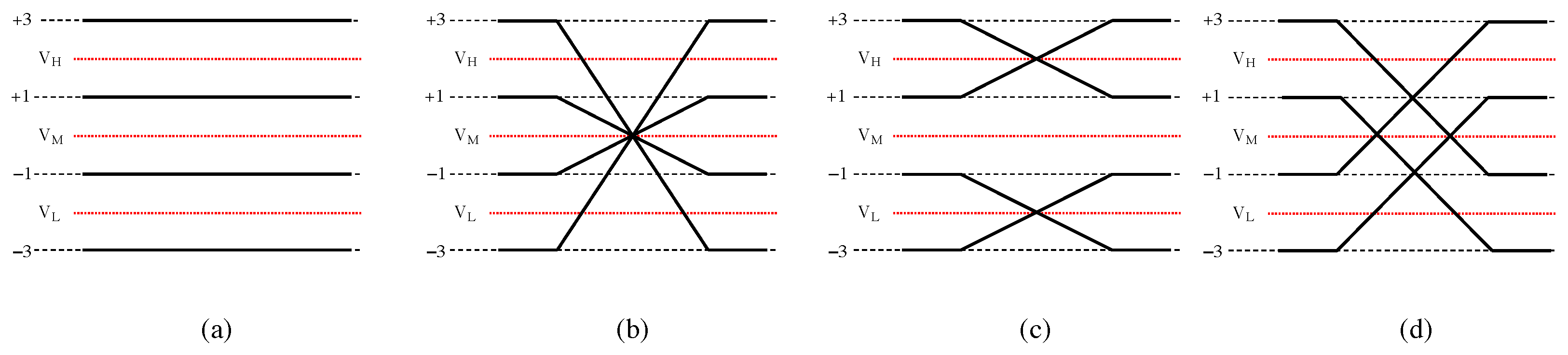
) with respect to PAM-2/NRZ coding, and the consequent reduction by a factor of two of the Nyquist frequency corresponds to lower channel attenuation and thus reduced ISI for the same data rate. One of the drawbacks, however, is that the use of four voltage levels complicates the architecture employed for phase detection and CDR. In fact, as can be seen in
Figure 1, there are 16 possible transitions between these four levels, but, as discussed below, care should be taken in how some of these transitions are handled when employing an Alexander bang-bang phase detector (PD) [
18].
Of course, the four transition types where the signal remains at the same level (
Figure 1a) do not provide any timing information. The symmetric transitions crossing the zero threshold (
Figure 1b) are the easiest to process and provide correct timing, also allowing the use of comparators with a zero threshold for edge detection. In fact,
transition filtering algorithms keep only these transitions and filter out all the others [
19].
Figure 1c shows transitions that are symmetric with respect to the high and low thresholds. These can be exploited if comparators with all three thresholds are available, adding complexity to the analog hardware operating at high speed. The transitions in
Figure 1d can lead to wrong Early/Late (E/L) information if not handled with care, since they are not symmetric. A possible countermeasure is to use a single comparator with a zero threshold and implement
partial filtering [
20]; this means that in the presence of jitter, 50% of these transitions (the
very early and
very late) are indeed useful. In the case of
multi-threshold architectures, all the transitions in
Figure 1d can be used by applying either majority voting or summation to the outputs of the three comparators [
21].
It is clear that the different options described above (multi-threshold, transition filtering, partial filtering and no filtering), by basing the detection of the E/L information on different sets of transitions, correspond to different bandwidths of the CDR loop. In this respect,
Figure 2 presents a linear model of a second-order CDR (left plot) and a sketch of the performance in terms of JTOL (right): using fewer transitions corresponds to lowering the open-loop gain of the system, thus leading to worse JTOL (see the expressions in
Section 3.4).
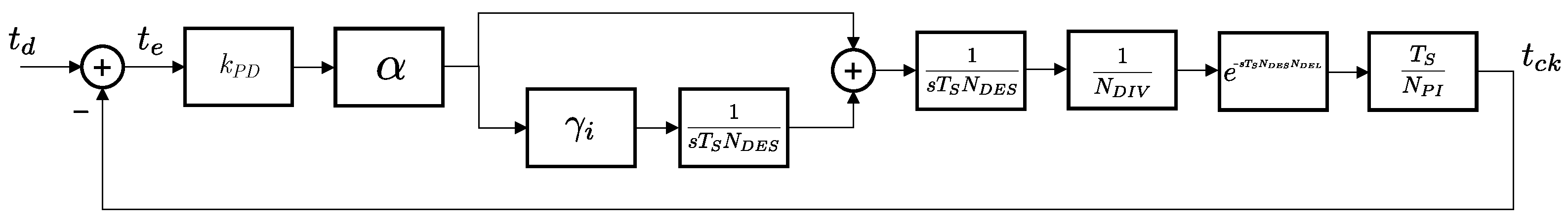
4. Results
In this section, we report simulation results for a 64 Gb/s PAM-4 HSSI with channel model and CDR architecture as described in
Section 3.2 and
Section 3.3. The aim is to show how the CDR parameters impact the JTOL performance. The prediction of the numerical model described in
Section 3.1 will be compared with the simple linear model described in
Section 3.4.
In this section, we assume that the frequency of the RX clock is exactly the same as that of the TX clock. Results with a frequency offset between the two are presented in
Appendix A.
The simulated eye diagram corresponding to the channel described in
Section 3.2 and the CDR whose parameters are listed in
Section 3.3 is reported in
Figure 7. Consistent with the cursors indicated in
Figure 4, we see that equalization has been effective in compensating ISI and the three eyes are open. We also see that the time aperture of the eyes is satisfactory (12 ps), meaning that the system jitter does not induce significant closing of the eyes.
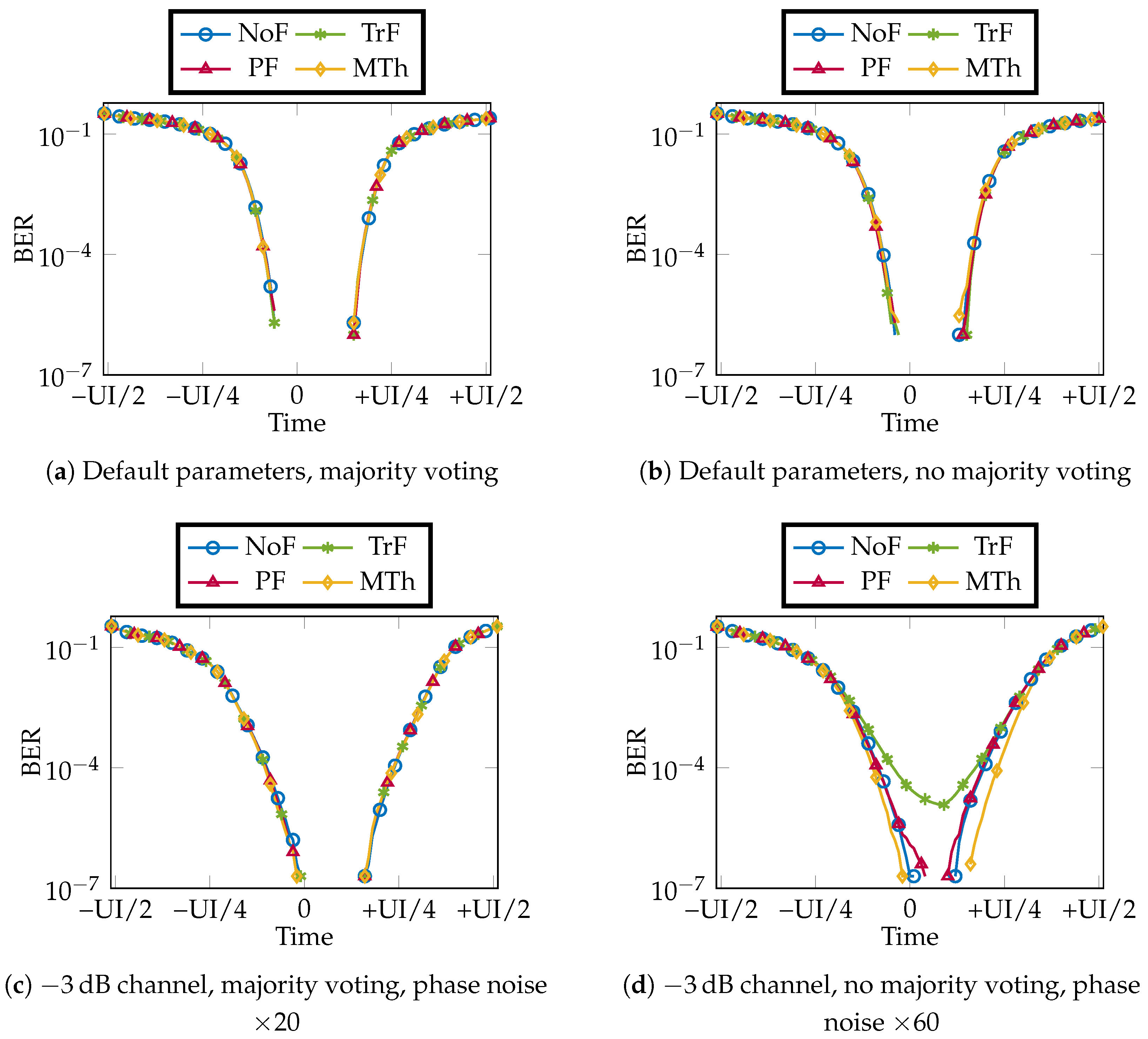
Before performing the JTOL analysis, we first simulate the receiver behavior without adding the sinusoidal jitter at the TX. The numerical model provides the bathtub plot, that is reported in
Figure 8 for a few cases. We see that the procedure makes it possible to determine BER values below 10
−6, and it is thus adequate for the PCIe 6.0 at 64 Gb/s. In
Figure 8a,b, we also see that, with the default CDR parameters of
Table 1, the results are hardly affected by the CDR algorithm, meaning that different transition filtering techniques, as well as the choice between using majority voting or summation on the
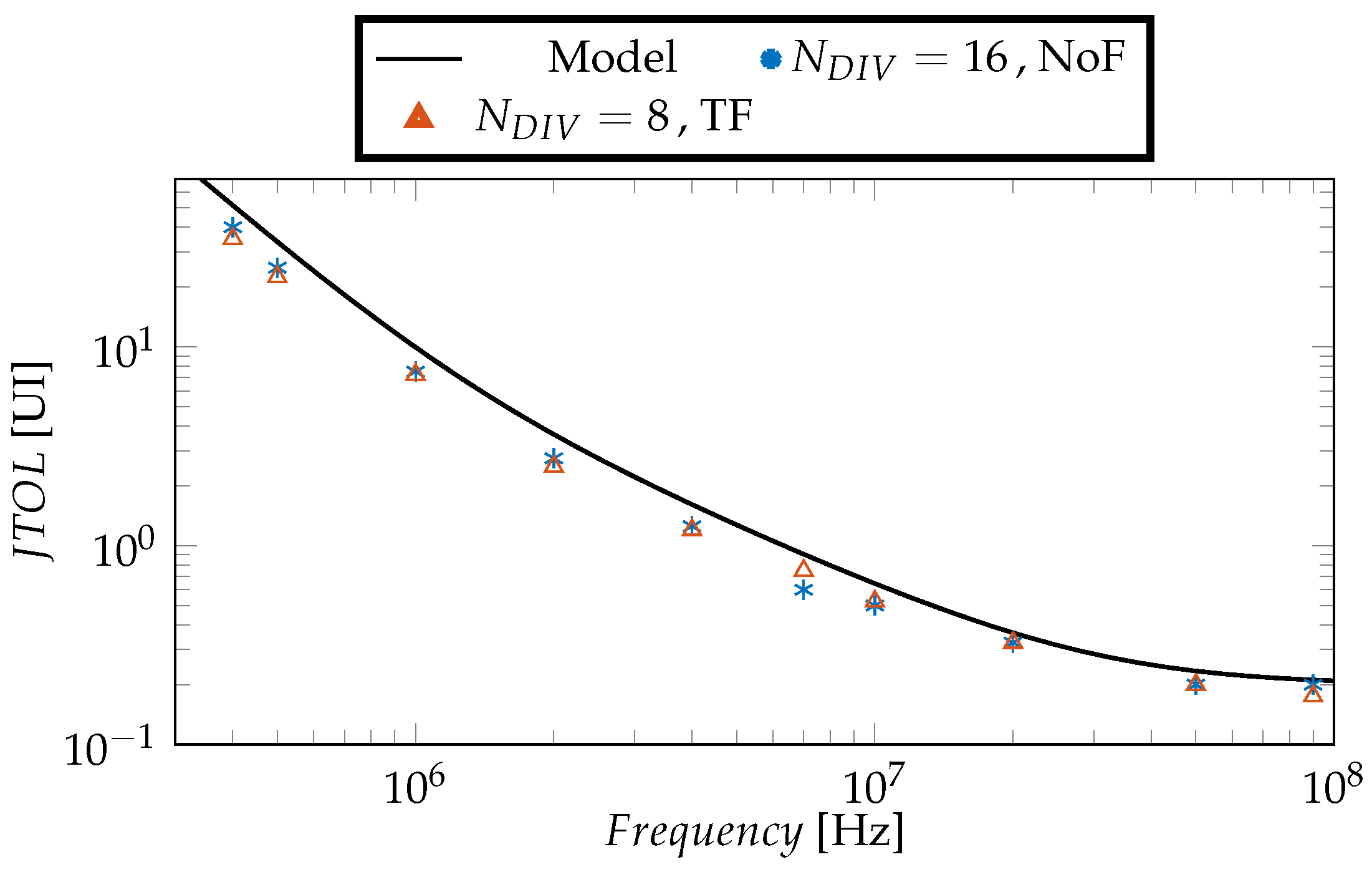
E/L signals coming from either one-threshold or three-threshold phase detectors, have a very limited influence on the bathtub.
These options essentially affect the CDR bandwidth, but this has limited influence on the jitter contributions related to channel ISI (the so-called
data-dependent jitter) and to the one due to the finite number of phases in the PI [
16] that dominates in our system. These jitter contributions are white and thus only marginally reduced by the high-pass characteristic of the CDR. Thus, to magnify the impact of the CDR bandwidth on the results we have increased the phase noise of the RX PLL and considered a channel with a much lower attenuation (3 dB), as can be seen in
Figure 8c,d. In particular, in the numerical experiment, the phase noise of the PLL is increased by a factor of 20 in the case of Majority Voting between the
E/L signals and by a factor of 60 when a sum over the E/L signals is performed. The data-dependent jitter due to the limited bandwidth of the channel has a negligible impact so that, in the bathtub plots, the major contribution is due to the oscillator’s phase noise that passes through the CDR’s high-pass transfer function. When performing Majority Voting over the deserialized E/L signals [
Figure 8c], the CDR bandwidth is not affected by the filtering algorithm, as will be extensively discussed in the following, such that the bathtub is essentially the same in all cases. Instead, if summation of the deserialized E/L signals is performed [
Figure 8d], the filtering algorithm clearly affects the CDR bandwidth and thus the bathtub.
Having shown that the choice of the transition filtering options and the choice between voting and summation of deserialized E/L signals have a minor impact on the jitter generated by the receiver (considering a channel with relevant ISI and thus large data-dependent jitter), we now analyze the JTOL performance. As seen in
Figure 2, JTOL also depends on the CDR bandwidth, which is directly linked to the capability of the loop to rapidly respond to misalignments between data and the clock and thus to making a decision based on as many transitions as possible. Therefore, we expect transition filtering to play a key role here.
We begin the investigation by considering a channel with negligible attenuation at Nyquist frequency (3 dB) instead of the one in
Figure 3 in order to separate the effect of CDR bandwidth from the reduced tolerance due to data-dependent jitter, which depends on ISI. This channel does not require any equalization.
Figure 9 shows the dependence of JTOL on some relevant CDR parameters considering summation between deserialized E/L signals. In plot (a), we vary
considering a multi-threshold phase detector: small values of this parameter result in large CDR bandwidths [
24] and thus better JTOL. We have verified that this holds also when varying
.
Figure 9b instead, analyzes the effect of
and
. The parameter
is the ratio between the gain of the integral and proportional paths (see Equation (
6) in
Section 3.4) and thus, according to
Figure 2, it controls the frequency at which the slope of JTOL changes from −2 to −1 (in logarithmic scales, i.e., decades of normalized UI versus decades of frequency). We see that for
, the region with slope −2 disappears and the parameter
does not have any impact on the results. On the other hand, for non-null
, smaller values of
result in better JTOL. The trends of
Figure 9a,b also hold for the other transition filtering options.
Figure 9c, instead, shows the influence on JTOL of the different CDR options discussed at the end of
Section 3.3: the ones exploiting more transitions result in better JTOL, as expected since more E/L signals are combined together. For all plots in
Figure 9, we see a good match between the numerical model of
Section 3.1 and the analytical model of
Section 3.4, meaning that the latter can be used to explain the main trends and to obtain back-of-the-envelope estimations of JTOL.
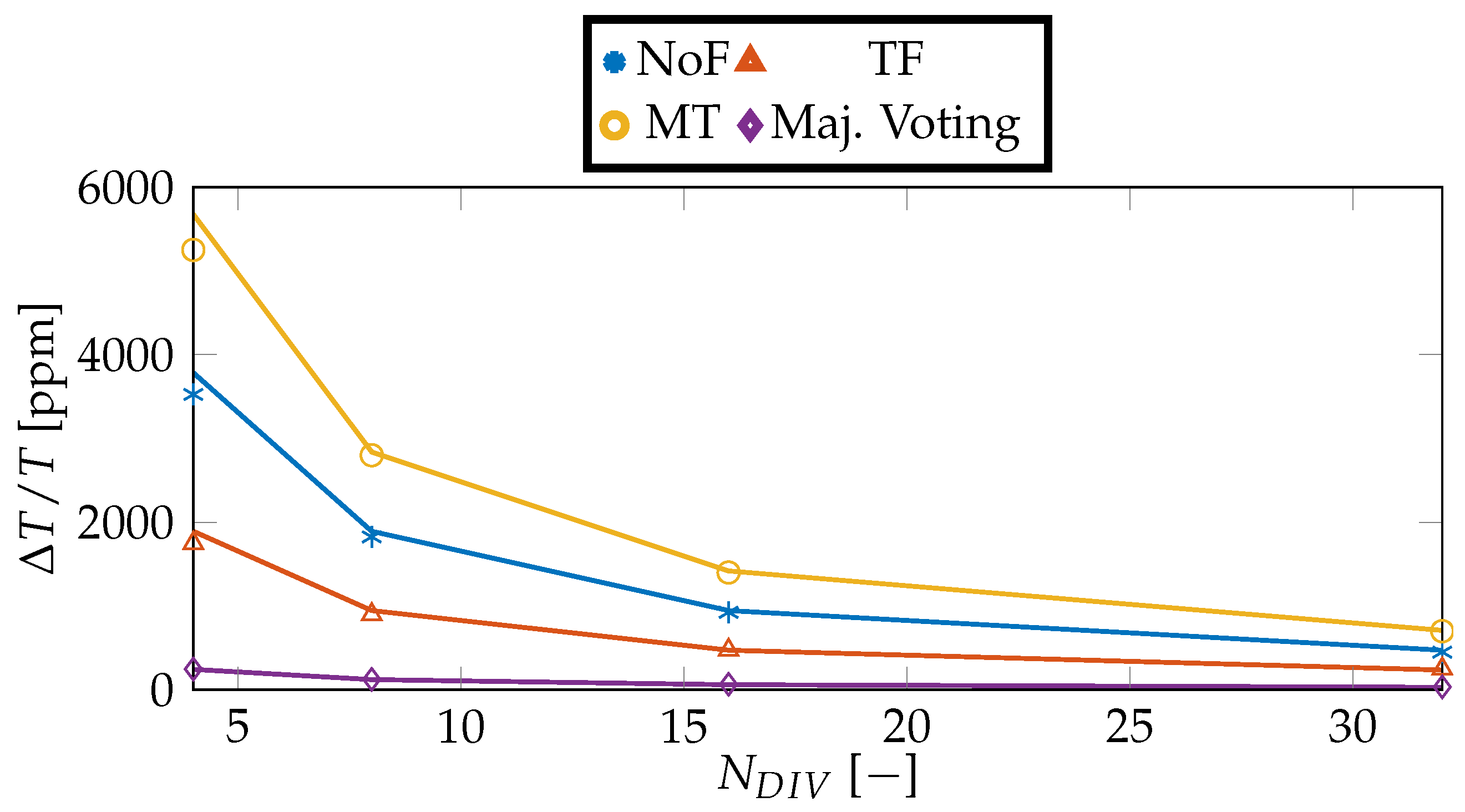
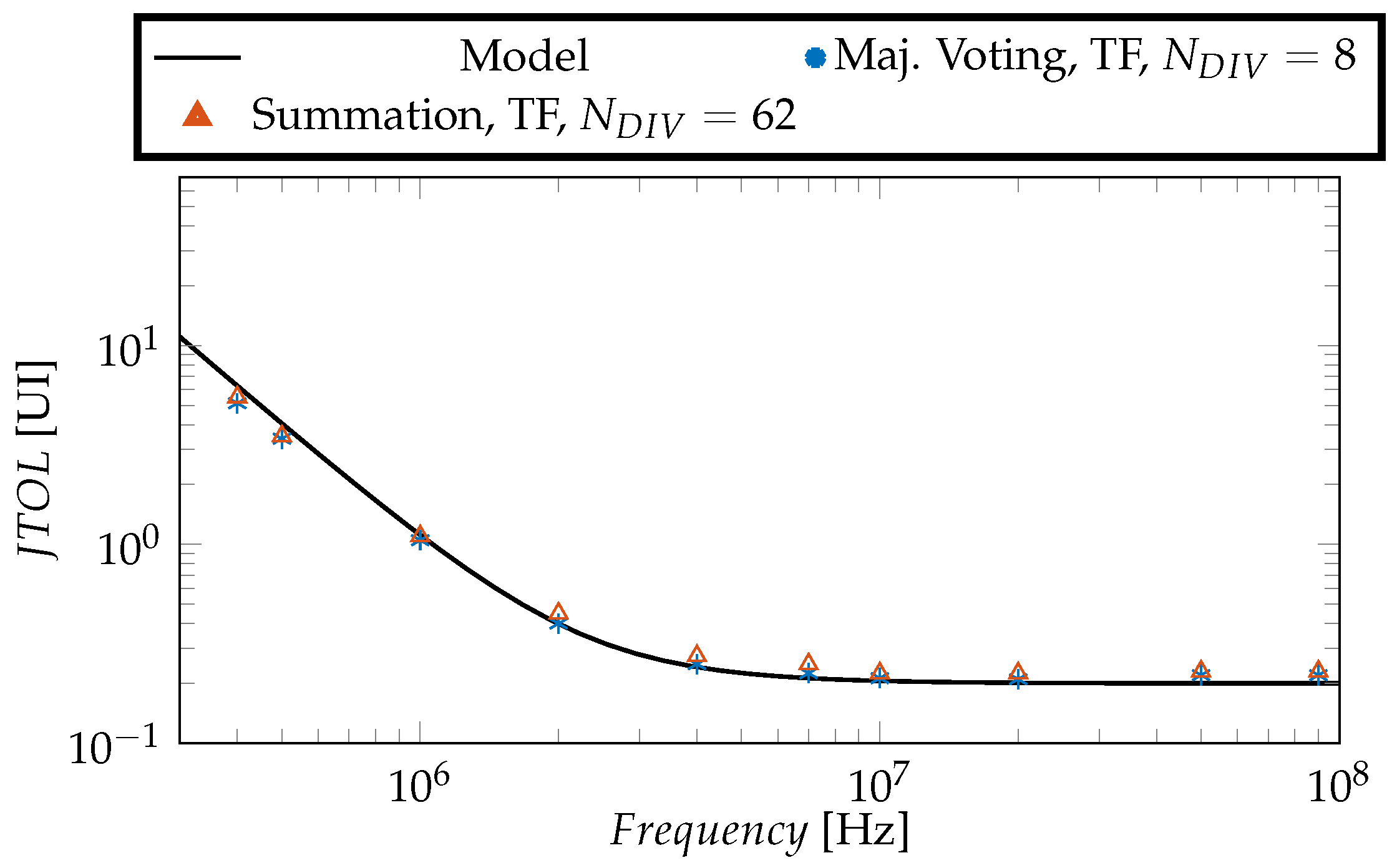
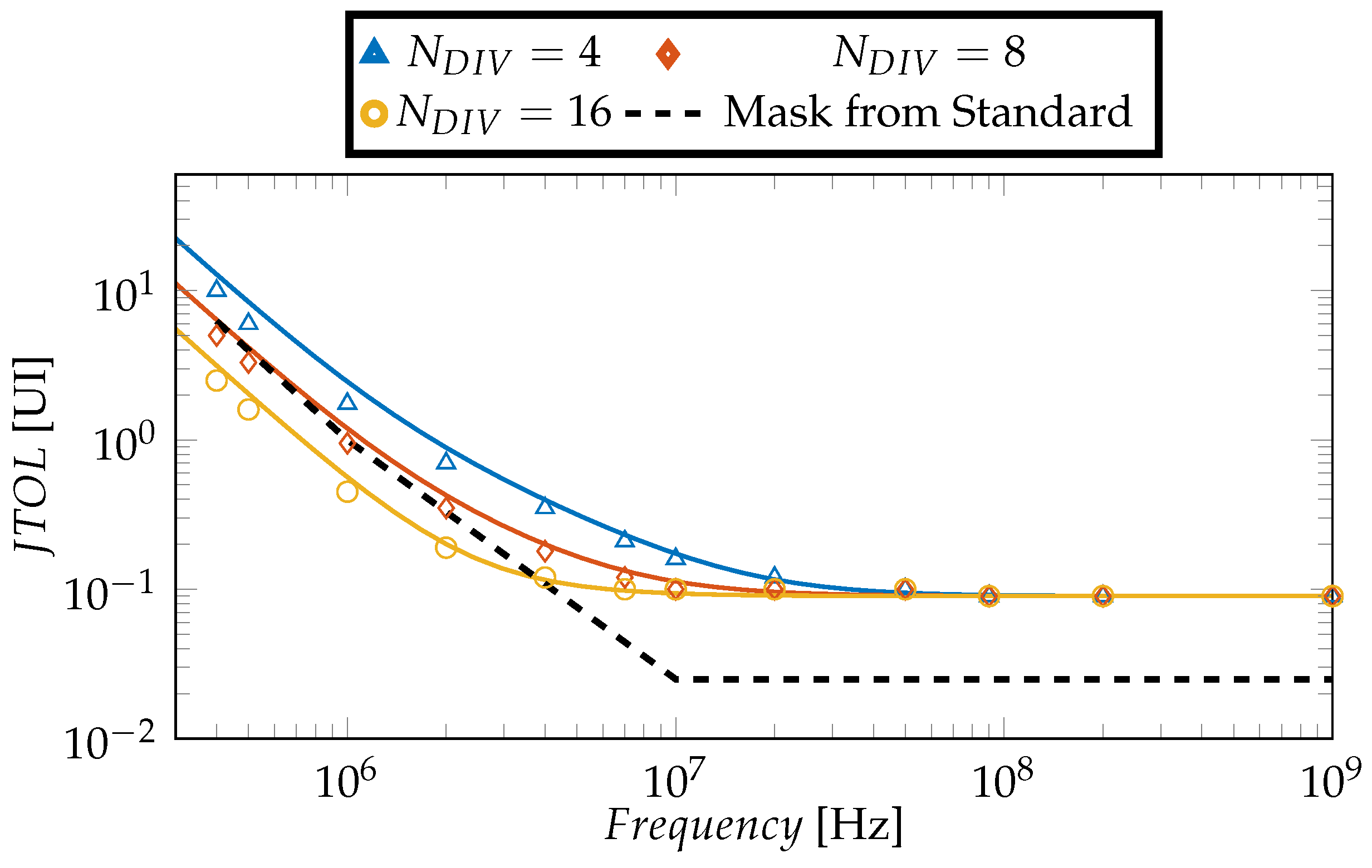
Figure 10 complements the analysis by considering a CDR implementing majority voting between the
E/L signals out of the PDs. The effect of
on JTOL is the same as in
Figure 9 and it is not reported again. On the other hand,
Figure 10a shows that
has a big effect, much larger than in the previous case: this is expected since we extract a single piece of E/L information out of
outputs of the PDs, resulting in a loss of bandwidth with respect to the case where the E/L signals out of the PDs are summed together. The case with
has been simulated considering the different filtering options, that however have no effect on JTOL. This is not surprising since, regardless of the filtering option, at least one piece of useful E/L information will come out from an array of 31 transitions. In fact, when we work with at least
, considering random data sequences, the case where no E/L is observed over a sequence of 16 deserialized symbols has a very low probability of occurring, and thus, its impact on JTOL would be very limited.
In
Figure 10b, we can observe the impact of the
factor, that, as in the previous analysis, sets the point where the slope of the JTOL curve changes from −2 to −1 (on a logarithmic scale). The impact of the parameter
on JTOL is limited, as shown in
Figure 10c, although
cannot be too large to prevent the JTOL at medium frequencies from deteriorating.
Figure 11 considers two sets of CDR parameters yielding the same bandwidth and plots the simulated JTOL considering a channel with 3 dB attenuation. The results further validate the model in Equation (
3), which closely matches the outcome of the time-domain numerical model. Two cases are considered: the blue markers represent a CDR with
without any filtering on the E/L signal outputs from the PD [which implies
], while the orange markers denote a configuration where transition filtering is performed on the E/L signals [that is
], hence compensating its loss in bandwidth by setting
, i.e., half the previous case. Not surprisingly, both configurations have the same JTOL characteristic, having the same bandwidth. The black solid line represents the model in Equation (
3), which obviously kept the same values for both the considered CDR configurations. The figure thus points out that the loss of bandwidth induced by the transition filtering can be compensated by reducing the division factor. The same applies if the bandwidth loss is compensated varying
. This analysis has been further extended considering two CDR configurations with either majority voting or summing of the
E/L signals out from the PDs, see
Figure 12. Similarly to
Figure 11, the loss in bandwidth due to majority voting (a loss of
) is compensated through a smaller
factor, resulting in the same JTOL characteristic. We have verified that the JGEN characteristic (i.e., the tails of the bathtub plot) does not change as well.
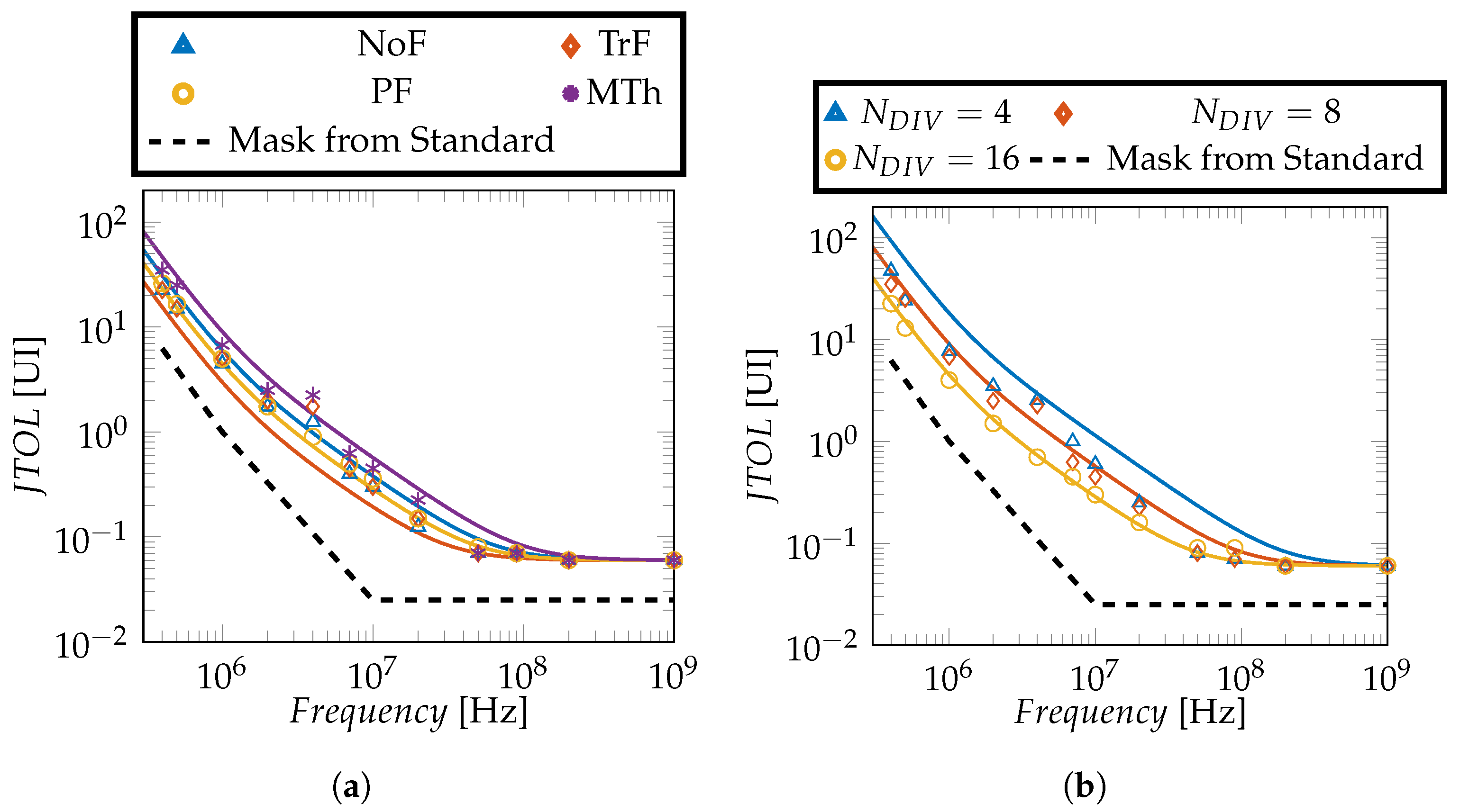
The trends observed using the channel with 3 dB attenuation at the Nyquist frequency have been confirmed by repeating the analysis using the channel of
Figure 3. Sample results are reported in
Figure 13 and
Figure 14, comparing the numerical time-domain model and the simple linear model of
Section 3.4 with the mask of the PCIe 6.0 standard [
17].
Figure 13a shows that, in this case as well, the transition filtering algorithm affects JTOL if summation between the E/L signals output by the PD is applied. Plot (b) instead shows that the influence of
is the same as in
Figure 9a. The same analysis is shown in
Figure 14 for the case of majority voting. The same results have been obtained regardless of the transition filtering algorithm. Comparison between
Figure 13b and
Figure 14 clearly shows that the use of majority voting of the deserialized E/L signals degrades JTOL performance at low frequency, whereas it slightly improves the JTOL value at high frequency (
value in
Figure 2, which is essentially the eye opening without sinusoidal jitter at the TX, as shown in
Section 3.4). In fact, as discussed in [
24], the summation of the deserialized E/L signals increases the CDR bandwidth but also amplifies the RX jitter associated with the finite number of PI phases. We also see that
in
Figure 13 and
Figure 14 is lower than in the cases with the 3 dB attenuation channel due to the presence of relevant data-dependent jitter associated with ISI. As a final remark, we see that the analytical model of
Section 3.4 nicely reproduces the simulation results, although in the case of
Figure 13 we had to artificially adjust the value of the PD gain by using
instead of the value
used in the other figures of the paper. This modification of the PD gain is reasonable since many mechanisms contribute to RX jitter in addition to the sinusoidal jitter applied at the TX. A proper model for the PD gain in such a situation can be found in [
26], but its inclusion in this analysis is beyond the scope of our work.
5. Discussion and Conclusions
We have analyzed the impact on JTOL of various CDR parameters and architectural choices in PAM-4 HSSIs. A time-domain numerical model has been employed and compared against the prediction of a simple linear model. The analysis has been mainly focused on the different transition filtering options used to derive the Early/Late information and on how to aggregate the array of deserialized E/L signals output by the phase detectors (majority voting vs. summation). It has been found that if majority voting is used, so that at least one useful transition is present in the array, then the features of the transition filtering algorithm are irrelevant and one can resort to a single comparator, without filtering the transitions.
On the other hand, summation significantly increases the bandwidth of the CDR loop, improving JTOL at low frequency, although the JTOL at high frequency (as well as the jitter contribution added by the CDR itself due to the finite number of PI phases) is degraded. When employing summation, applying transition filtering reduces the CDR bandwidth with respect to algorithms exploiting more transitions. In any case, the bandwidth is larger than when performing majority voting of the deserialized E/L signals. Furthermore the reduction of the CDR bandwidth due to transition filtering can be compensated by lowering the value of the divider placed in the loop.
These results may appear in contrast with those in [
15], but one should consider that the CDR architecture considered in that work differs from the ones analyzed here. First, CDR is applied to baud rate data and edge samples. Secondly, a VCO is used instead of a PI (as in our analysis) to generate the aligned clock. This makes the jitter in [
15] more affected by the quantization noise of the PD, while, in our system, the quantization noise of the PI dominates. When the PD quantization noise dominates, the reduction of the CDR gain induced by transition filtering can be indeed compensated by increasing the gain of the following blocks (divider, etc). This compensates JTOL but results in an amplification of the PD quantization noise. In our architecture, this does not occur, and any bandwidth reduction due to transition filtering can be compensated.
The simulation framework that has been developed is quite general and makes it possible to investigate the impact of any CDR parameter on JTOL and JGEN. Although, in this paper, many blocks have been assumed to be ideal, it is almost straightforward to include in the model effects such as offset and delay of the comparators, non-linearity of the PI and duty-cycle errors in the clock.


 ,
, 


