Article

A 50 Gb/s 0.42 pJ/b Non-Return-to-Zero Transmitter for Extra-Short-Reach SerDes

by
Lili Sun
,
Zhongxu Jin
,
Yanchao Liu
,
Xiaohua Yu
and
Ronghua Ni
*
State Key Laboratory of Integrated Chips and Systems, Institute of Microelectronics, Fudan University, Shanghai 201203, China
*
Author to whom correspondence should be addressed.
Electronics 2025, 14(10), 1955; https://doi.org/10.3390/electronics14101955
Submission received: 8 April 2025 / Revised: 1 May 2025 / Accepted: 8 May 2025 / Published: 11 May 2025

Abstract

An energy- and area-efficient non-return-to-zero (NRZ) transmitter with feedforward equalization (FFE) is proposed for an extra-short-reach (XSR) data interface in chiplet-based system in packages (SiPs) and multi-chip modules (MCMs). At the system level, the final-stage 2:1 multiplexer (MUX) in the transmitter is combined with the driver to reduce the hardware and power consumption; at the circuit level, charge-steering-based moderate-swing signal processing further reduces the circuit power consumption and inter-symbol interference. Fabricated in a 28 nm CMOS process with a core area of 0.032 mm2, the prototype NRZ transmitter demonstrates an energy efficiency of 0.42 pJ/b at a data rate of 50 Gb/s with an insertion loss of 10 dB, which makes it a promising candidate for XSR die-to-die (D2D) interfaces.

1. Introduction

With the rapid advancement of artificial intelligence (AI), machine learning (ML), and hyperscale computing, the amount of data that need to be manipulated and transported increases exponentially [1,2,3,4]. While improving the yield of a single chip, allowing process optimization of each die, and reducing the cost of the whole system, the chiplet-based system in package (SiP) and multi-chip module (MCM) technology impose stringent requirements on the data communication between dies [5,6,7]. With a usual insertion loss of less than 10 dB, the extra-short-reach (XSR) die-to-die (D2D) interface requires data lanes with a large data rate, compact area, and small power consumption, where NRZ encoding is preferred for its relaxed SNR requirement, less circuit complexity, and lower power consumption [8]. Meanwhile, appropriate equalization such as feedforward equalization (FFE) has been proven to play an important role in the signal bandwidth extension in wireline communication, and its adjustable equalization weights are crucial for addressing different channels [9]. By leveraging system- and circuit-level innovations, a power- and area-efficient non-return-to-zero (NRZ) transmitter with FFE is proposed in this paper, which makes it a promising candidate for XSR D2D interfaces.
The most challenging and power-hungry part of the transmitter consists of the 4:1 MUX and channel driver because they operate at the highest frequency. In the traditional architecture, as shown in Figure 1a [10], the front end of the transmitter consists of a 4:1 data MUX followed by a retiming flip-flop driven by the full-rate clock to align and send the data to the driver. The data retiming using a full-rate clock requires large power consumption to meet the timing specification. Therefore, it is favored to eliminate the full-rate flip-flops and align the data using multi-phase clocks at a half-rate or quarter-rate for an improved energy efficiency. As shown in Figure 1b, the main path and FFE path data are multiplexed by two sequential stages of 2:1 MUX before the driver. In this structure, the data retiming is achieved by a 50% duty cycle half-rate clock at the second-stage 2:1 MUX. Both the second-stage 2:1 MUX and the driver manipulate the data at their full rate; the current of the two parts will be very large and therefore dominate the power consumption of the whole system [11]. The combination of the 4:1 MUX and the driver is proposed in [12] to minimize the blocks that operate at high frequency. As shown in Figure 1c, to combine 4:1 multiplexing and FFE, eight differential pairs of transistors merge at the output node of the driver, resulting in excessive parasitic capacitance. Therefore, a more complicated bandwidth extension network is required at the driver output that involves multiple inductors with large inductance values, which significantly increases the chip area. Furthermore, a half-rate clock with a 25% duty cycle is required for the single-stage 4:1 multiplexing. The circuit of the 25% duty cycle generation consumes more power and deteriorates the data eye diagram due to the duty cycle mismatch.
The proposed transmitter architecture is shown in Figure 1d: low power and a compact area are achieved by levering the following techniques at both the system and circuit levels. At the system level, the final-stage 2:1 MUX is incorporated into the current mode logic (CML) driver. To maintain the same CML output swing, the current consumed in this combined 2:1 MUX and driver module is equal to the current of the output driver in Figure 1b. Therefore, the 2:1 MUX power consumption is saved in the proposed structure compared to that in Figure 1b. On the other hand, the combination of the 2:1 multiplexing and driver in the proposed structure introduces much less parasitic capacitance at the output node compared to the 4:1 MUX and driver architecture in Figure 1c; therefore, a simple series inductance peaking can be utilized to mitigate the bandwidth penalty, resulting in both low power consumption and a small area. At the circuit level, instead of maintaining the full-swing signals in the conventional CMOS transmitter architecture, a signal path with a moderate swing is adopted in this transmitter to save the power consumption. This is achieved by the charge-steering logic (CSL)-based 4:2 MUX followed by a CML driver combined with the 2:1 MUX. Because the CSL circuits operate with moderate data swings while drawing power for only a fraction of the clock cycle, they afford a design faster than rail-to-rail logic [13]. Please note that a CML driver instead of an inverter-based driver is chosen in this design for the following reasons. First, the NMOS input CML driver accommodates the common mode voltage of the preceding CSL MUX outputs, which is closer to VDD. Second, the CML driver can accept and amplify moderate-swing signals while the inverter-based driver usually needs power-hungry pre-drivers to achieve a near full-swing input signal [5]. Last but not least, more slices are needed to make FFE programmable in an inverter-based driver, which introduces more parasitic capacitance at the driver output nodes [14].
The main contents are organized as follows. Section 2 explains in detail the whole transmitter architecture. Section 3 explains the specific circuit designs. Section 4 describes the measurement setup and results, followed by the conclusion in Section 5.

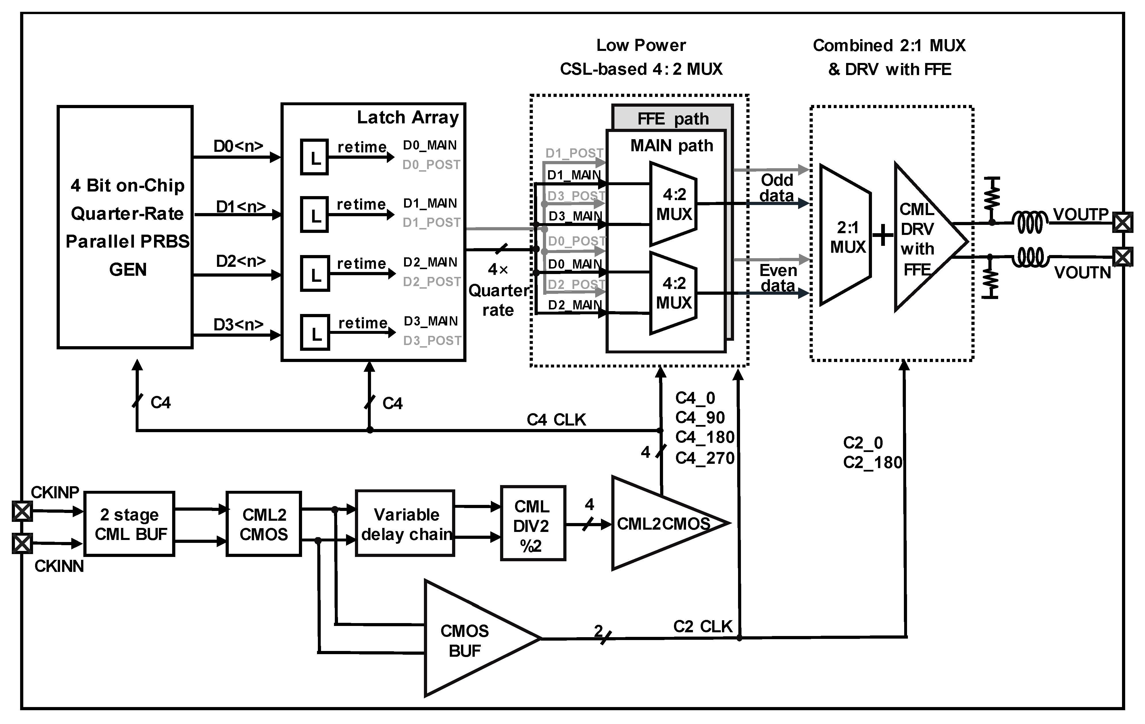
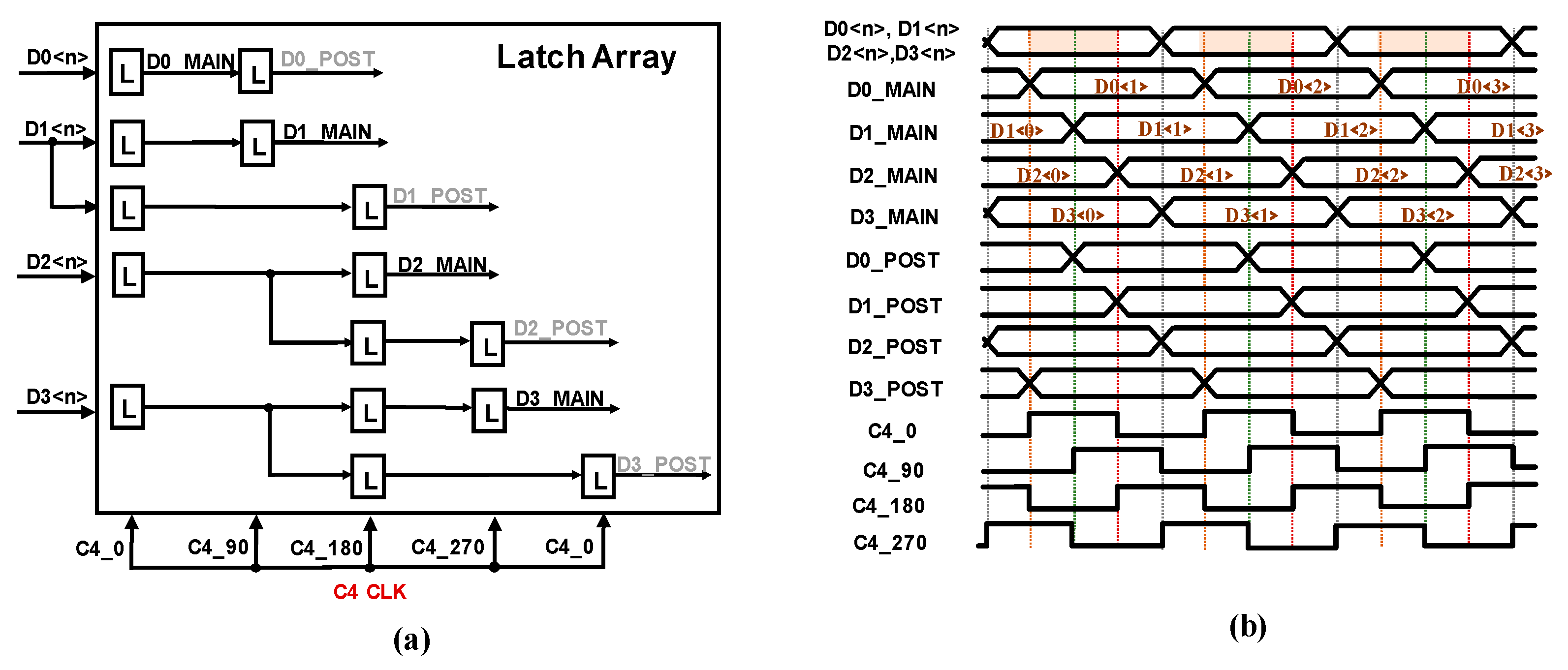
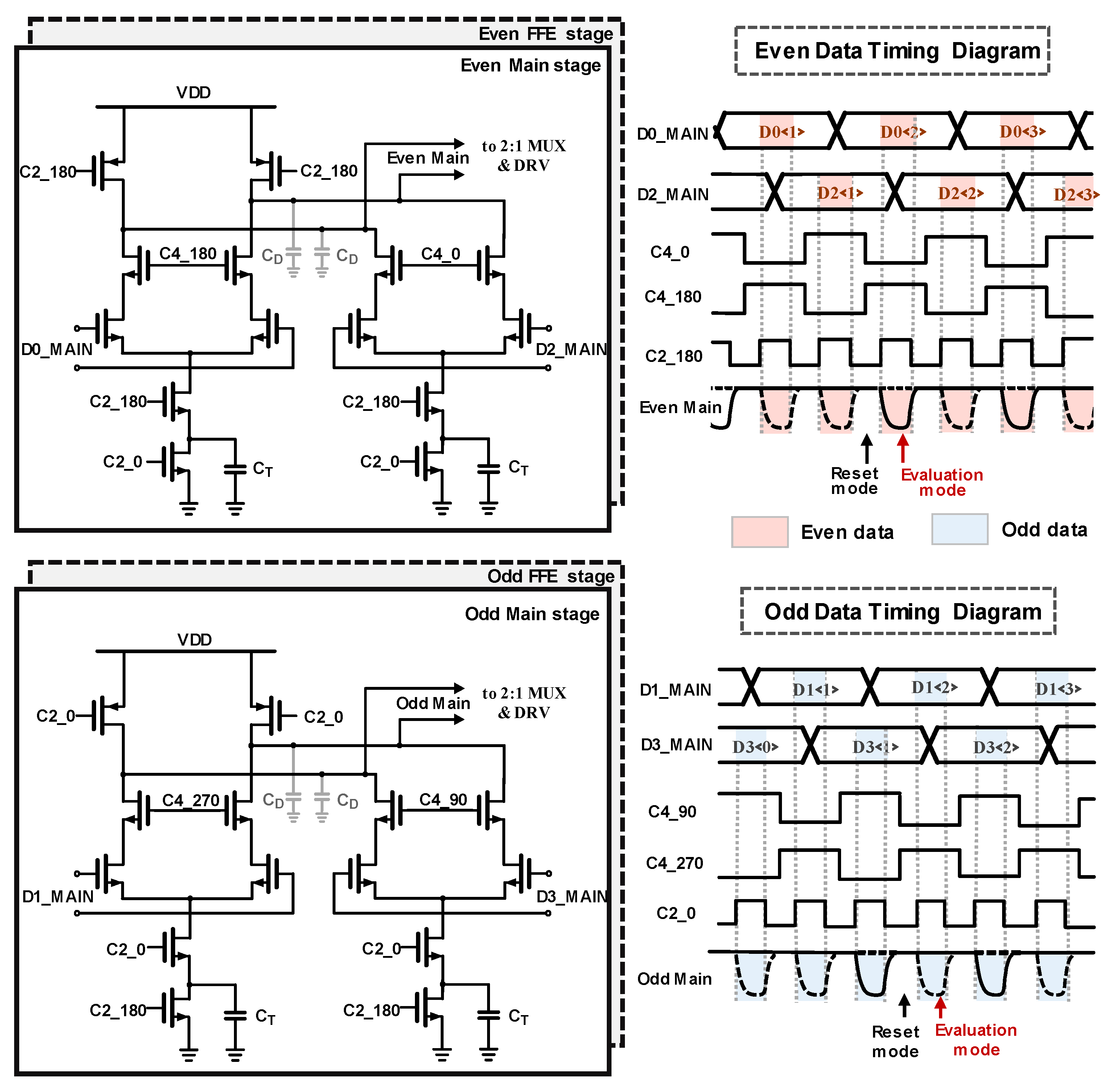
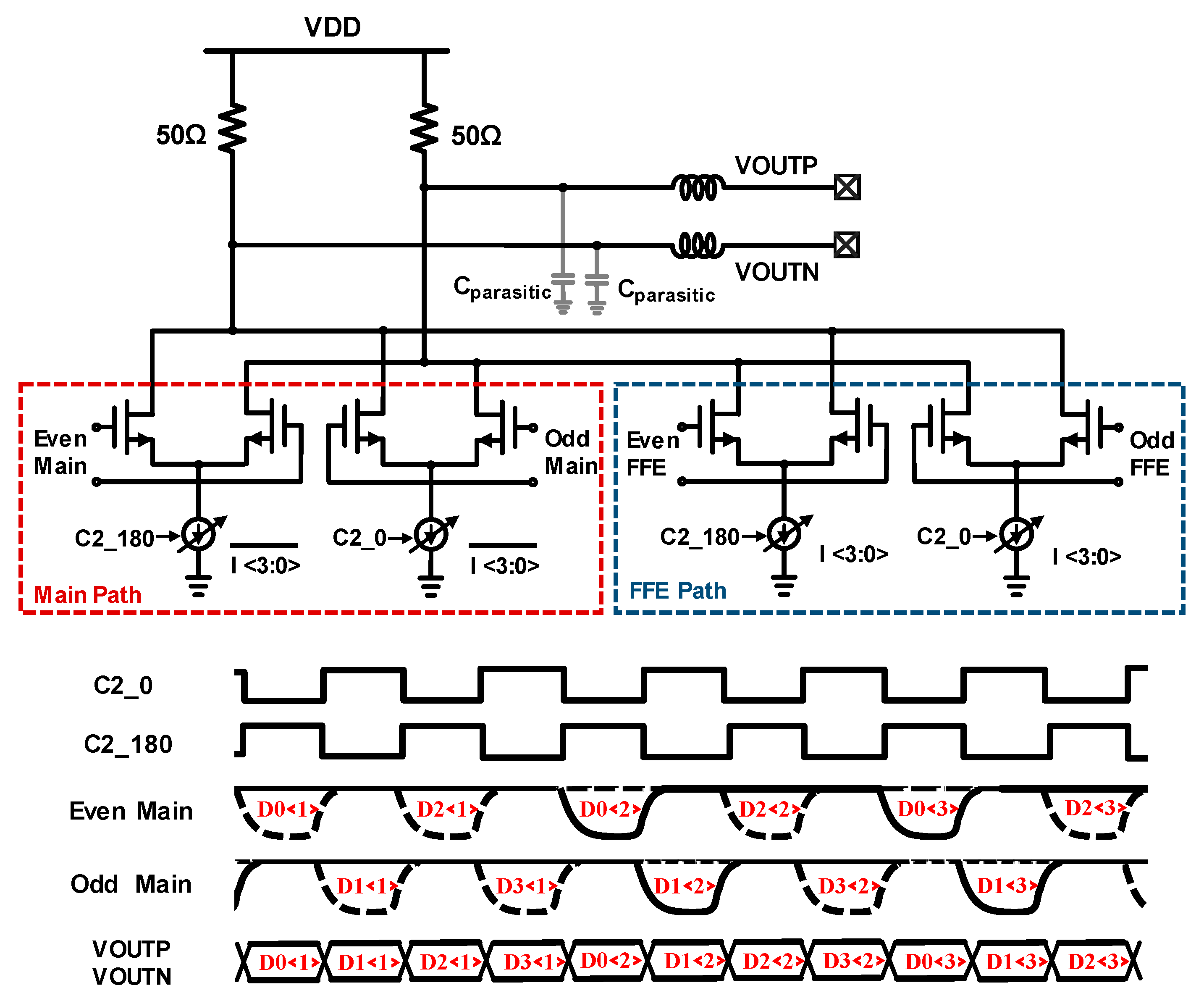
2. Architecture of Transmitter

The overall architecture of the proposed transmitter is shown in Figure 2. In the signal path, an on-chip four-bit pseudo-random binary sequence (PRBS) generator is implemented to generate four parallel paths of the PRBS7 sequence. A latch array driven by four-phase quarter-rate clocks (C4) is designed to retime the data with a maximized timing margin for the subsequent 4:2 MUX. Meanwhile, since the rising edge of the previous phase and the next phase clock triggers the latch to generate the main path data and FFE path data, respectively, the FFE data path with one unit interval (UI) delay is also generated in the latch array with the same timing margin as the main data path. The following CSL-based 4:2 MUX serializes the data in both main and FFE paths, and the half-rate data are sent to the combined 2:1 MUX and driver, which is driven by C2 clocks to complete the final serialization. The FFE weighting is made four-bit-programmable to optimize the equalization for different channel loss. Furthermore, a series inductor is utilized to mitigate the bandwidth degradation due to the capacitive loading at the driver output nodes. In the clock path, the differential half-rate clocks C2 are generated through an external balun and the four-phase quarter-rate clocks C4 are generated through a CML divider-by-2. A variable delay chain is introduced in the clock path before the CML DIV2 to optimize the timing margin between the four-phase clocks (C4 CLK) and the data path. The clock chain is simulated with process, voltage, and temperature (PVT) variations to ensure the reliability of the design.

3. Circuit Implementation

The system structure and timing diagram of the latch array is shown in Figure 3. It receives four parallel data paths (D0<n>, D1<n>, D2<n>, D3<n>) from the preceding PRBS generator and retimes the data for both main (D0_MAIN, D1_MAIN, D2_MAIN, D3_MAIN) and FFE (D0_POST, D1_POST, D2_POST, D3_POST) paths for the following 4:2 MUX. The circuit of the latch consists of a transmission gate followed by an inverter. As shown in Figure 3, with the input data aligned with C4_270, the first stage of latches clocked by C4_0 sample the input data at the middle of the data window, maximizing the timing margin and reducing the latch speed requirement. The sequential-phase clocks (C4_90, C4_180, and C4_270) sample the data generated by the preceding phases, rendering the same optimal timing margin for all the four-path output data. Please note that, with an extra latch clocked by a clock 90 degrees later, the FFE path data can be generated from the corresponding math path data with the same optimal timing margin.
Reducing the data swing helps to reduce the power consumption and inter-symbol interference (ISI) in the MUX design. In this work, a CSL-based MUX is designed for low-power 4:2 multiplexing. The CSL circuits maintain moderate signal swings and draw power for only a fraction of the clock cycle; therefore, they can achieve a faster speed than rail-to-rail circuits and draw less power than current mode logic circuits. The detailed circuit of the 4:2 MUX and its corresponding timing diagram is depicted in Figure 4. Taking the even main path as an example (as shown on the top of Figure 4), the MUX toggles between reset mode and amplification mode, which is controlled by C2_180 and C2_0. Meanwhile, the output data are chosen between D0_MAIN and D2_MAIN, dictated by C4_180 and C4_0. Therefore, the output of the even main stage is return-to-zero (RZ) half-rate even data. With appropriate clock assignment, the output of the odd main stage (as shown at the bottom of Figure 4) is RZ half-rate odd data with 1UI delay compared to the even main path. Therefore, the output data of the even and odd main stage can be multiplexed in the following stage to obtain the fully serialized data. It is worth noting that the gain and output swing of the CSL-based MUX are closely related to the ratio of CT and CD [13], where CT is the tail capacitance and CD is the capacitance of the output node. Meanwhile, the size of the CT value is also closely related to the speed of the circuit. When one of the input transistors is turned on, the charge accumulated at the output node during the reset mode will be redistributed between the CD and CT. Therefore, the larger the CT, the lower the voltage at the source of the input transistor, resulting in a larger VGS and VDS of the input MOS, thus making the CSL-based 4:2 MUX operate faster. In this design, the value of CT and CD are 56f and 13f, respectively, which is designed to consider the output swing and circuit speed.
In order to achieve efficient data processing and transmission, the circuit of the combined 2:1 MUX and driver with FFE is adopted and shown in Figure 5, where the last-stage 2:1 MUX is integrated with the output driver. Selected by C2_180 and C2_0, respectively, the even and odd paths of the data are serialized into the final full-rate data. As shown in the timing diagram of the main path in Figure 5, the driver samples the odd main data when C2_0 is high and samples the even main data when C2_180 is high. In this way, the even and odd paths of the data are multiplexed into the final full-rate data in the driver stage under the drive of the half-rate clock. Meanwhile, the tail currents of both the main and FFE path are controlled by four-bit digital signals to implement a programmable FFE weighting, which accommodate it for different channel responses. In this 2:1 MUX and driver combined circuit, the average current drawn from the power supply is the same as that of a conventional CML driver [15] for the same output signal swing, therefore saving the extra power consumption in the preceding 2:1 MUX shown in Figure 1b. It is worth noting that a current mode driver instead of an inverter-based voltage mode driver is chosen in this design because the output of the CSL-based MUX is a moderate-swing signal with a common-mode voltage closer to VDD. The output network consists of a 50-ohm loading resistor with a series peaking inductor, which extends the signal bandwidth with the presence of a parasitic capacitor at the driver output nodes. The series peaking technique has been proven to have a very good bandwidth extension ratio [16].

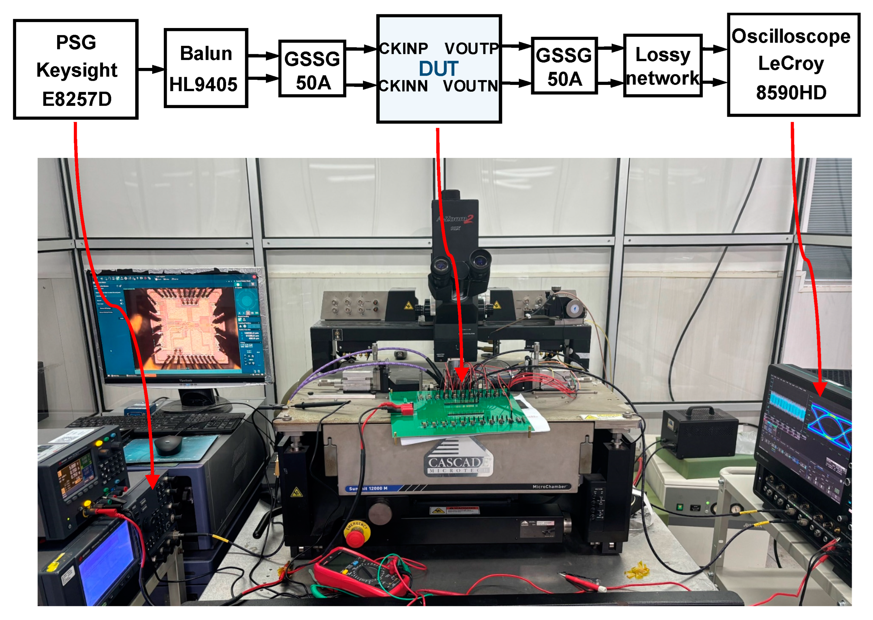
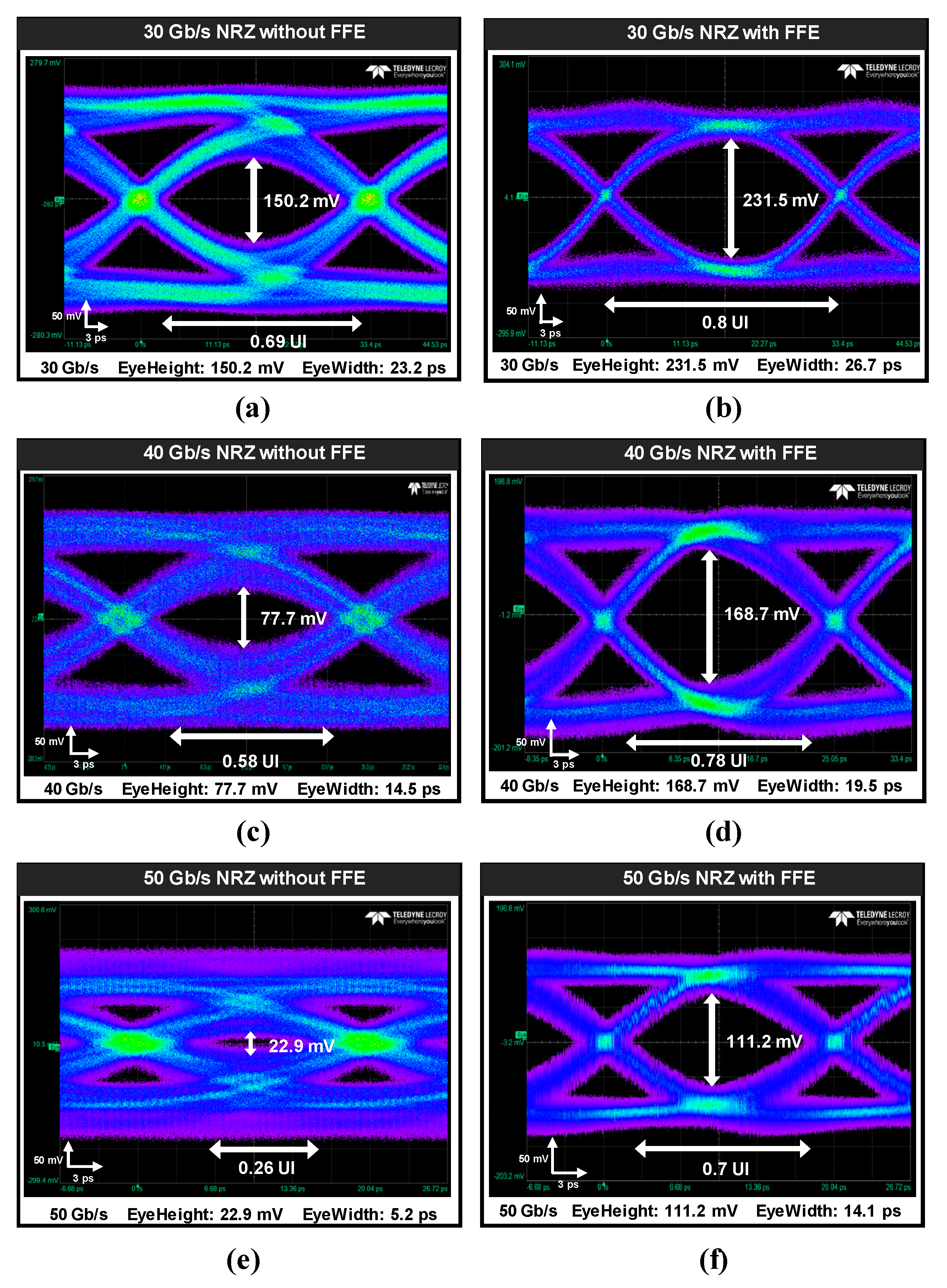
4. Measurement Results and Discussion

The proposed NRZ transmitter is designed and fabricated with 28 nm CMOS technology. The chip micro-photograph is shown in Figure 6, with a core area of 0.032 mm2, including all the blocks listed in the table on the right. For power integrity, decoupling caps are added on the chip between power supplies and the ground to mitigate the power supply ripples introduced by the bonding wire inductance.
The measurement setup is shown in Figure 7. The transmitter die is chip-on-board-packaged on a daughter board, which is mounted on an RF probe station for high-speed connection. The power supplies and control signals are generated on a motherboard and connected to the daughters through wires. The half-rate clock is generated by the Keysight E8257D, which is converted from single-ended to differential through a balun HL9405 with a bandwidth of up to 50 GHz. The clock signal is transmitted through connectors and cables, and is delivered to the RF probe (GGB Picoprobe 50A) with the same bandwidth of 50 GHz. The transmitter output data are measured through the 50A RF probe, 48-inch cables, DC blocks, and connectors of the real-time oscilloscope (Teledyne LeCroy 8590HD), which introduces 10 dB loss at 25 GHz.
The measured eye diagrams of the proposed transmitter at a data rate of 30–50 Gb/s with and without FFE are shown in Figure 8. At the data rate of 30 Gb/s, the measured eye height increases from 150.2 mV to 231.5 mV and the measured eye width increases from 0.69 UI to 0.8 UI when FFE is turned on. At the data rate of 40 Gb/s, the measured eye height increases from 77.7 mV to 168.7 mV and the measured eye width increases from 0.58 UI to 0.78 UI when FFE is turned on. When the data transmission rate is further increased to 50 Gb/s, the measured eye height increases from 22.9 mV to 111.2 mV and the measured eye width increases from 0.26 UI to 0.7 UI when FFE is turned on, as shown in Figure 8e,f. Meanwhile, the performances of the transmitter under various PVT corners were also verified in the post-simulation, which shows the reliability of this work.
The frequency response of the transmitter output network in the measurement is shown in Figure 9a, showing a loss of 10 dB at the Nyquist frequency of 25 GHz. The power breakdown of the transmitter at 50 Gb/s is shown in Figure 9b. During the measure, by dividing the VDD of each module and testing the current flowing through each module, the corresponding power consumption can be calculated. Excluding the PRBS generator and clock path, the total power consumption in the data path is 21 mW, achieving an energy efficiency of 0.42 pJ/b.
Table 1 summarizes and compares the measured performance of the designed transmitter with some state-of-the art transmitters. The smallest core area combined with the lowest data path energy efficiency makes it a promising candidate for future die-to-die applications.

5. Conclusions

This paper proposes a power- and area-efficient NRZ transmitter for XSR SerDes. At the system level, the final 2:1 MUX is combined with the driver to save the hardware and power consumption compared to traditional designs, and a simple single-inductance series peaking network effectively extends the signal bandwidth in the presence of the parasitic capacitance at the driver output nodes. At the circuit level, CSL-based moderate-swing signal processing further reduces the power consumption and inter-symbol interference. The prototype transmitter demonstrates a data path energy efficiency of 0.42 pJ/b with a core area of 0.032 mm2 at a data rate of 50 Gb/s, which makes it a promising candidate for low-power and small-area XSR wireline communication applications such as chip-to-chip and die-to-die data interfaces.

Author Contributions

Conceptualization, L.S.; writing—original draft preparation, L.S.; methodology, L.S.; validation, Z.J.; investigation, Z.J.; data curation, Y.L.; supervision, X.Y.; writing—review and editing, R.N.; project administration, R.N. All authors have read and agreed to the published version of the manuscript.

Funding

This research received no external funding.

Data Availability Statement

All data are available on request from the corresponding author.

Acknowledgments

The use of instruments in the chip measurement process was supported by Teledyne LeCroy Incorporated.

Conflicts of Interest

The authors declare no conflicts of interest.

References

  1. Seong, K.; Oh, W.; Lee, H.; Bae, G.; Suh, Y.; Lee, H.; Kim, J.; Kim, E.; Kang, Y.; Mo, G.; et al. 13.10 A 4 nm 48 Gb/s/wire Single-Ended NRZ Parallel Transceiver with Offset-Calibration and Equalization Schemes for Next-Generation Memory Interfaces and Chiplets. In Proceedings of the 2024 IEEE International Solid-State Circuits Conference (ISSCC), San Francisco, CA, USA, 18–22 February 2024; pp. 250–252. [Google Scholar]
  2. Liu, Q.; Wang, H.; Lyu, F.; Zhang, G.; Lyu, D. A low-latency, low-jitter retimer circuit for PCIe 6.0. Electronics 2023, 12, 3102. [Google Scholar] [CrossRef]
  3. Suhani S.H., A.A.; Prasad S., N.; Reddy, K.S.S. A 20 Gb/s Latency Optimized SerDes Transmitter for Data Centre Applications. In Proceedings of the IEEE International Conference on Electronics, Computing and Communication Technologies (CONECCT), Bangalore, India, 2–4 July 2020; pp. 1–4. [Google Scholar]
  4. Wu, J.Y.; Chen, C.H.; Lee, C.H.; Liu, C.S.; Yu, D.C.H. SoIS-An Ultra Large Size Integrated Substrate Technology Platform for HPC Applications. In Proceedings of the 2021 IEEE 71st Electronic Components and Technology Conference (ECTC), San Diego, CA, USA, 1 June–4 July 2021; pp. 28–33. [Google Scholar]
  5. Seong, K.; Park, D.; Bae, G.; Lee, H.; Suh, Y.; Oh, W.; Lee, H.; Kim, J.; Lee, T.; Mo, G.; et al. A 4 nm 32 Gb/s 8Tb/s/mm Die-to-Die Chiplet Using NRZ Single-Ended Transceiver with Equalization Schemes And Training Techniques. In Proceedings of the 2024 IEEE International Solid-State Circuits Conference (ISSCC), San Francisco, CA, USA, 19–23 February 2023; pp. 114–116. [Google Scholar]
  6. Park, J.H.; Lee, H.; Cho, H.; Lee, S.; Lee, K.H.; Ko, H.G.; Jeong, D.K. A 32 Gb/s/pin 0.51 pJ/b Single-Ended Resistor-less Impedance-Matched Transmitter with a T-Coil-Based Edge-Boosting Equalizer in 40 nm CMOS. In Proceedings of the 2024 IEEE International Solid-State Circuits Conference (ISSCC), San Francisco, CA, USA, 19–23 February 2023; pp. 410–412. [Google Scholar]
  7. Hsu, Y.Y.; Kuo, P.C.; Chuang, C.L.; Chang, P.H.; Shen, H.H.; Chiang, C.F. A 7 nm 0.46 pJ/bit 20 Gbps with BER 1E-25 Die-to-Die Link Using Minimum Intrinsic Auto Alignment and Noise-Immunity Encode. In Proceedings of the 2021 Symposium on VLSI Circuits, Kyoto, Japan, 13–19 June 2021; pp. 1–2. [Google Scholar]
  8. Lee, J.; Chiang, P.C.; Peng, P.J.; Chen, L.Y.; Weng, C.C. Design of 56 Gb/s NRZ and PAM4 SerDes Transceivers in CMOS Technologies. IEEE J.-Solid-State Circuits 2015, 50, 2061–2073. [Google Scholar] [CrossRef]
  9. Ye, B.; Wu, G.; Gai, W.; Sheng, K.; He, Y. A Five-Tap Delay-Line-Based Feed-Forward-Equalizer for 200-Gb/s Wireline Receiver in 28-nm CMOS. IEEE J.-Solid-State Circuits 2024, 59, 19–28. [Google Scholar] [CrossRef]
  10. Hafez, A.A.; Chen, M.S.; Yang, C.K.K. A 32–48 Gb/s Serializing Transmitter Using Multiphase Serialization in 65 nm CMOS Technology. IEEE J.-Solid-State Circuits 2015, 50, 763–775. [Google Scholar] [CrossRef]
  11. Zheng, X.; Zhang, C.; Lv, F.; Zhao, F.; Yuan, S.; Yue, S.; Wang, Z.; Li, F.; Wang, Z.; Jiang, H. A 40-Gb/s Quarter-Rate SerDes Transmitter and Receiver Chipset in 65-nm CMOS. IEEE J.-Solid-State Circuits 2017, 52, 2963–2978. [Google Scholar] [CrossRef]
  12. Sheng, K.; Gai, W.; Feng, Z.; Niu, H.; Ye, B.; Zhou, H. 6.7 A 128 Gb/s PAM-4 Transmitter with Programmable-Width Pulse Generator and Pattern-Dependent Pre-Emphasis in 28 nm CMOS. In Proceedings of the 2024 IEEE International Solid-State Circuits Conference (ISSCC), San Francisco, CA, USA, 19–23 February 2023; pp. 120–122. [Google Scholar]
  13. Jung, J.W.; Razavi, B. A 25-Gb/s 5-mW CMOS CDR/Deserializer. IEEE J.-Solid-State Circuits 2013, 48, 684–697. [Google Scholar] [CrossRef]
  14. Song, E.; Han, J.; Seo, H.; Kim, H.; Im, H.; Han, J. A 35-Gb/s PAM-4 Transmitter with 7B4Q Full-Transition Avoidance and Area-Efficient Gm-Boosting Techniques. IEEE Trans. Circuits Syst. II Exp. Briefs 2024, 71, 46–50. [Google Scholar] [CrossRef]
  15. Gu, Y.; Chen, J.; Li, X.; Chen, Y.; Wu, J. A 32 Gb/s NRZ Wireline Transmitter with CMFB-Based CML Driver in 28 nm CMOS Technology. In Proceedings of the 2021 IEEE International Midwest Symposium on Circuits and Systems (MWSCAS), Lansing, MI, USA, 9–11 August 2021; pp. 14–17. [Google Scholar]
  16. Shekhar, S.; Walling, J.S.; Allstot, D.J. Bandwidth Extension Techniques for CMOS Amplifiers. IEEE J.-Solid-State Circuits 2006, 41, 2424–2439. [Google Scholar] [CrossRef]
  17. Toprak-Deniz, Z.; Proesel, J.E.; Bulzacchelli, J.F.; Ainspan, H.A.; Dickson, T.O.; Beakes, M.P. A 128-Gb/s 1.3-pJ/b PAM-4 Transmitter with Reconfigurable 3-Tap FFE in 14-nm CMOS. IEEE J.-Solid-State Circuits 2020, 55, 19–26. [Google Scholar] [CrossRef]
  18. Celik, F.; Akkaya, A.; Tajalli, A.; Leblebici, Y. A 32-Gb/s PAM-4 SST Transmitter with Four-Tap FFE Using High-Impedance Driver in 28-nm FDSOI. IEEE Trans. Very Large Scale Integr. (VLSI) Syst. 2021, 29, 1132–1140. [Google Scholar] [CrossRef]
  19. Wu, W.; Wu, H.; Zhong, L.; Cheng, X.; Luo, X.; Xu, D.; Wang, C.; Li, Z.; Pan, Q. A 64 Gb/s/pin Single-Ended PAM-4 Transmitter with a Merged Preemphasis Capacitive-Peaking Crosstalk Cancellation Scheme for Memory Interfaces in 28-nm CMOS. IEEE J.-Solid-State Circuits 2025, 60, 205–216. [Google Scholar] [CrossRef]
Figure 1. Transmitter with (a) full-rate clock-driven flip-flop. (b) Half-rate clock-driven 2:1 MUX. (c) A 4:1 MUX combined with driver driven by 25% duty cycle half-rate clock. (d) The proposed half-rate clock-driven 2:1 MUX combined with driver.
Electronics 14 01955 g001
Figure 2. Overall architecture of the proposed transmitter.
Electronics 14 01955 g002
Figure 3. (a) The system structure and (b) timing diagram of the latch array.
Electronics 14 01955 g003
Figure 4. Circuit and timing diagram of the CSL-based 4:2 MUX.
Electronics 14 01955 g004
Figure 5. Circuit and timing diagram of the combined 2:1 MUX and driver with FFE.
Electronics 14 01955 g005
Figure 6. Chip micro-photograph.
Electronics 14 01955 g006
Figure 7. Measurement setup.
Electronics 14 01955 g007
Figure 8. Measured transmitter output eye diagrams: (a) 30 Gb/s without FFE; (b) 30 Gb/s with FFE; (c) 40 Gb/s without FFE; (d) 40 Gb/s with FFE; (e) 50 Gb/s without FFE; (f) 50 Gb/s with FFE.
Electronics 14 01955 g008
Figure 9. (a) Insertion loss of the transmitter output network. (b) Power breakdown in data path.
Electronics 14 01955 g009
Table 1. Performance comparison of advanced transmitters.
[11][12][14][17][18][19]This Work
Process [nm]65282814282828
Data rate [Gb/s]40128356432326450
Supply [V]1.2N/A1.250.951N/A0.9
SignalingNRZPAM4PAM4NRZPAM4NRZPAM4NRZ
Driver TypeCMLCMLSSTCMLSSTSSTCML
Equalization4-tap FFE4-tap FFE2-tap FFE3-tap FFE4-tap FFE3-tap FFE2-tap FFE
IL@Nyquist Frequency6 dB4 dB5.2 dB6 dBN/A11 dB10 dB
Test PRBS length7N/A731N/AN/A7
Eye Height [mV]18044101N/A3818036111.2
Eye Width [UI]0.680.20.68N/A0.160.60.360.7
Power * [mW]74115166.8513937.75621
Energy Efficiency *
[pJ/bit]
1.850.94.762.11.1780.8750.42
Area [mm2]0.60.1370.180.0480.080.0850.032
* The data path excluding clock path and PRBS generator. N/A means not reported.
Disclaimer/Publisher’s Note: The statements, opinions and data contained in all publications are solely those of the individual author(s) and contributor(s) and not of MDPI and/or the editor(s). MDPI and/or the editor(s) disclaim responsibility for any injury to people or property resulting from any ideas, methods, instructions or products referred to in the content.

