Article

S-SP Inductive Power Transfer System with High Misalignment Tolerance Based on a Switch-Controlled Capacitor

School of Electronic Information Engineering, Xi’an Technological University, 2, Xuefu Rd., Xi’an 710021, China
*
Author to whom correspondence should be addressed.
Electronics 2025, 14(1), 188; https://doi.org/10.3390/electronics14010188
Submission received: 22 November 2024 / Revised: 24 December 2024 / Accepted: 31 December 2024 / Published: 5 January 2025

Abstract

:
In order to reduce the sensitivity of an inductive power transfer (IPT) system to the misalignment coupling coil, an S-SP-compensated IPT system with high misalignment tolerance based on a switch-controlled capacitor (SCC) is proposed. Firstly, the mathematical model of the S-SP compensation topology is established, the output characteristics and impedance characteristics of the system are analyzed, and a sensitivity analysis of the compensation element parameters is carried out using the compensation topology. An improved switching capacitor structure is proposed to dynamically compensate the S-SP IPT system. Finally, an experimental prototype was set up to validate the correctness of the theoretical analysis. The experimental results show that the proposed method can ensure that the system can operate in the resonant state with high efficiency when the coupling pad’s horizontal misalignment is within 30% (with the coupling coefficient varying from 0.22 to 0.14).

1. Introduction

An inductive power transfer (IPT) system can facilitate the transfer of electrical energy from the primary side to the secondary side through electric and magnetic fields, thereby enabling a non-contact power supply between the power source and the load [1,2,3]. Compared with wired transmission, this transmission mode has the advantages of safety and reliability, and can be applied in a wide range of scenarios. At present, it has been applied in smart homes, wearable electronic devices, electric vehicles, and other fields [4,5,6].
In the IPT system, the coupling coil plays an important role as the medium for capacity transmission. The transmitting coil is excited by the alternating power source generated by the inverter and the receiving coil obtains electric energy from the transmitting coil. However, in practical applications, it is often challenging to perfectly align the secondary receiving coil with the transmitting coil in typical magnetic resonance wireless charging systems [7]. This misalignment leads to significant fluctuations in the coupling mutual inductance between the coils. Consequently, the transmission characteristics will change, and the system transmission efficiency will decrease due to the influence of coil coupling variations. In order to reduce the influence of coil offset on the output voltage and output efficiency, a large amount of research has been carried out, mostly focusing on the control strategy, magnetic coupling design, hybrid topology design, and parameter optimization design.
Various control strategies, such as DC-DC converters [8,9], phase shift control, and variable frequency control [10,11,12,13,14], have been proposed to ensure stable output. A semi-active rectifier was used on the secondary side to achieve a constant voltage output. The proposed method can ensure a 72V output under load variations of 30 to 60 Ω [8]. To achieve a relatively stable output power in situations of misalignment and load, a multiphase multifrequency system is proposed in [14]. However, these closed control methods usually need wireless communications, which may result in increased volume, increased cost, and instability problems. A magnetic coupling design, such as tripolar pads, double-D pads, quadruple-D pads, etc., can avoid the above-mentioned disadvantages [15,16,17,18,19]. In order to create an omnidirectional wireless charging system [15], three orthogonal coils are used to provide a strong magnetic flux density. Two objective problems of pad optimization are discussed in [19], involving their optimized design, shape, and size. Hybrid topologies, combining compensation networks with opposite output characteristics, have also been proposed to maintain a stable output power [20,21,22]. However, these hybrid topologies usually need many resonant capacitance and coupling pads, which may result in a complex design and cost. Parameter optimization design, an alternative method, can enable a steady output [23,24,25]. An S-SP compensation topology with parameter design was proposed to increase the tolerance for misalignments [23]. A detuned S-S-compensated IPT system was presented to provide stable output power during variations in coupling [24]. However, these detuned parameter optimization methods can provide misalignment capabilities at the price of system efficiency because these systems usually operate in a detuned state. Therefore, it is necessary to operate in a resonant state and improve the misalignment tolerance without the need for complex control and wireless communication.
To address the aforementioned challenges, an S-SP topology with a switched capacitor converter is proposed to achieve stable output. The S-SP topology combines the serial resonance compensation topology and series–parallel resonance compensation topology. A mathematical model and sensitivity analysis of the S-SP topology are detailed. The improved switched capacitor structure is then adopted to tune the compensation topology under misalignment conditions. Additionally, control algorithms are proposed to dynamically adjust the equivalent capacitance of parallel compensation capacitors on the secondary side by modulating the conduction angle. Finally, a prototype is constructed to validate the correctness and feasibility of the theoretical analysis.

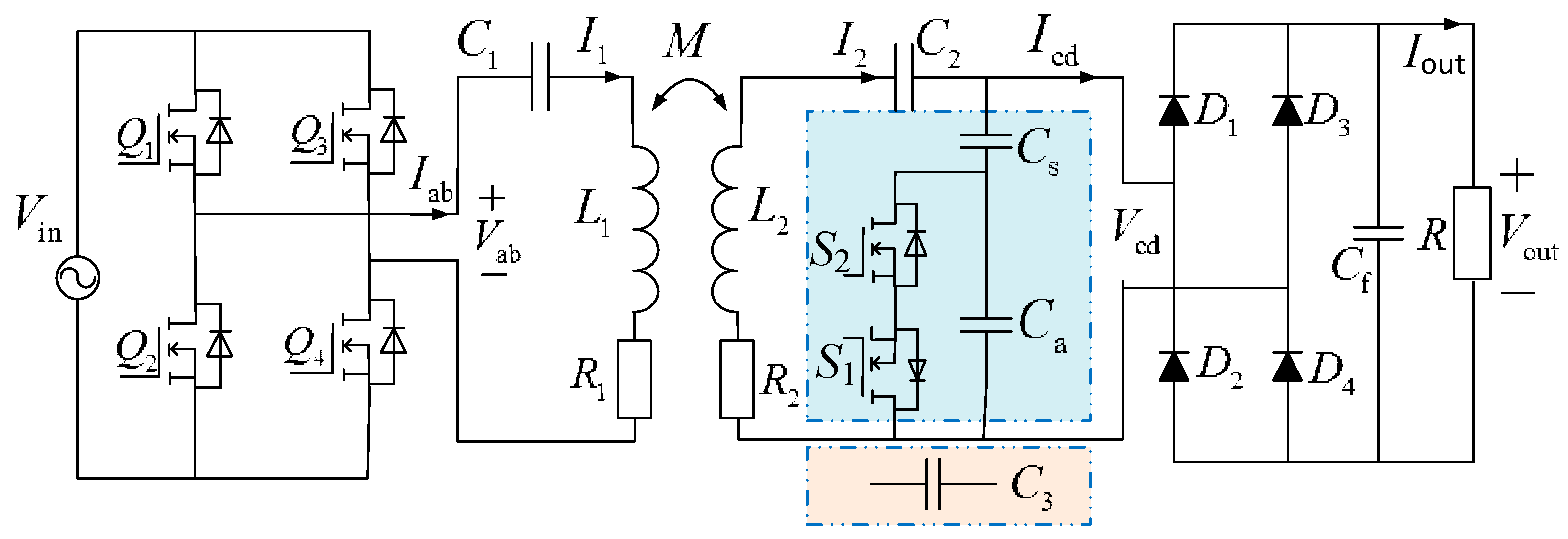
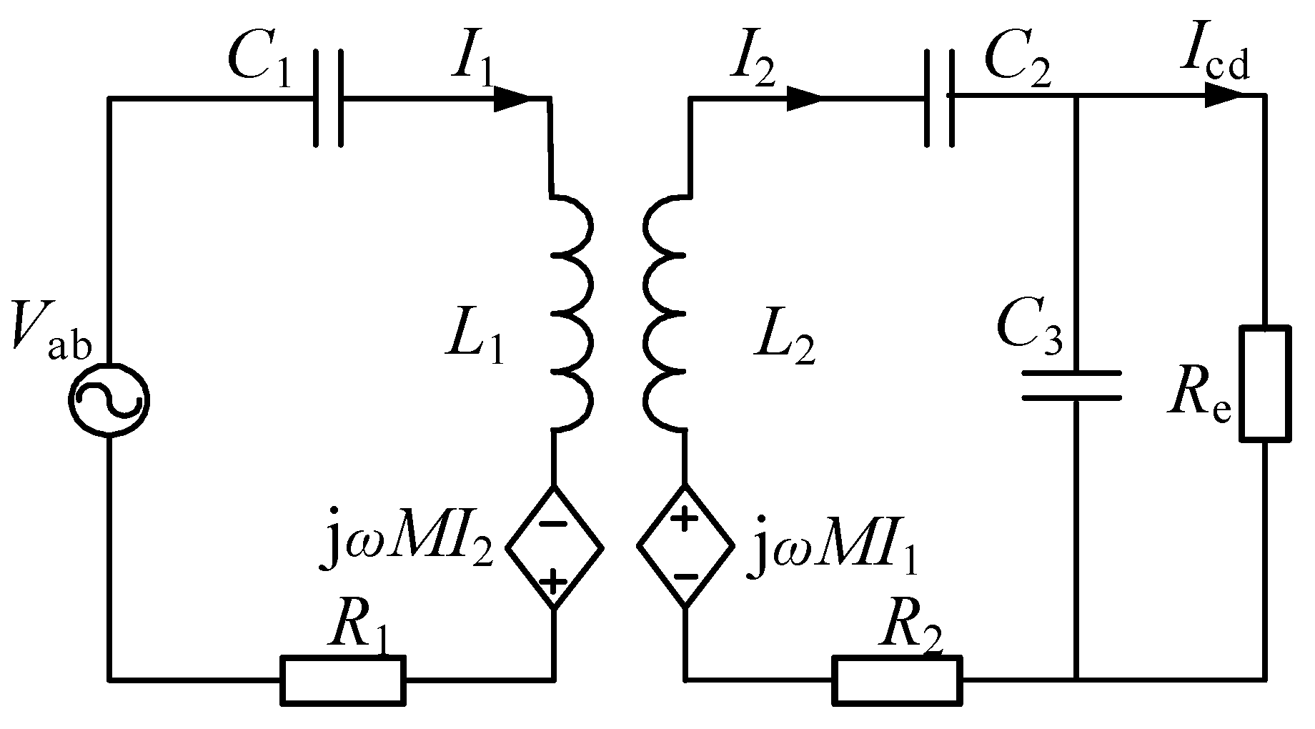
2. S-SP Compensation Topology Theoretical Analysis

2.1. S-SP’s Fully Tuned State

Figure 1 shows the S-SP compensation topology based on a switched capacitor structure. Uin is the DC power supply, which inputs a constant DC voltage to the high-frequency inverter. Q1–Q4 constitutes a full-bridge inverter, which converts the input DC voltage into high-frequency AC. D1–D4 forms the rectifier and the capacitor Cf acts as the filter capacitor, supplying a stable DC voltage to the load. L1 and L2 represent the inductance of the primary and secondary coils; C1 is the primary compensation capacitor; and C2, Ca, and Cs are the secondary compensation capacitors, which can be equivalent to C3. S1 and S2 are the reversed series MOSFETs. I1 is the input current of the primary side, I2 is the input current of the secondary side, and Icd is the output current. Figure 2 shows the equivalent S-SP compensation topology. Re is the equivalent load on the AC side, which can be expressed as Re = 8R2 [23].
Based on KVL, the equations of the system can be expressed as follows:
V ab = Z 1 I 1 j ω M I 2 0 = ( Z 2 + Z 3 ) I 2 Z 3 I cd j ω M I 1 0 = ( Z 3 + R e ) I cd Z 3 I 2
where
Z 1 = j ω L 1 + 1 j ω C 1 + R 1 Z 2 = j ω L 2 + 1 j ω C 2 + R 2 Z 3 = 1 j ω C 3
To alleviate stress on passive components, the system operates in a resonant state. The operating angular frequency can be designed as follows:
ω = 1 L 1 M C 1 = 1 L 2 M C 2 = 1 M C 3
The current I1, I2, and I0 can be obtained from (1):
I 1 = V ab R e R 2 + ω M j R 2 + ω M R e R 1 R 2 + j ω M R e R 1 R 2 + ω 2 M 2 R e + R 1 + R 2 I 2 = ω M V ab j R e + ω M R e R 1 R 2 + j ω M R e R 1 R 2 + ω 2 M 2 R e + R 1 + R 2 I cd = ω 2 M 2 V ab R e R 1 R 2 + j ω M R e R 1 R 2 + ω 2 M 2 R e + R 1 + R 2
Therefore, the output voltage gain Gv can be calculated from (3):
G v = M 2 ω 2 R e R e R 1 R 2 + j M R e R 1 R 2 ω + M 2 R e + R 1 + R 2 ω 2
and the input impedance can be calculated as
Z in = R e R 1 R 2 + j M R e R 1 R 2 ω + M 2 R e + R 1 + R 2 ω 2 R e R 2 + M ω j R 2 + M ω
When ignoring the parasitic resistance, the compensated topological input phase angle can be obtained as follows:
θ = a r c t a n I m [ Z in ] R e [ Z in ] = a r c t a n ω R C 2 + C 3 1 + C 2 L 2 ω 2 1 C 2 L 2 ω 2
From (4) and (6), the output voltage gain and input phase angle curves are shown in Figure 3.
Figure 3 illustrates that the output voltage gain Gv remains constant at the resonant angular frequency ω0 regardless of changes in the equivalent load, indicating the proposed S-SP topology can provide constant voltage output. Additionally, the input phase angle θ is consistently zero at this resonant frequency. This results in an input impedance that is purely resistive, reducing reactive power loss and ensuring maximum output power and transmission efficiency.

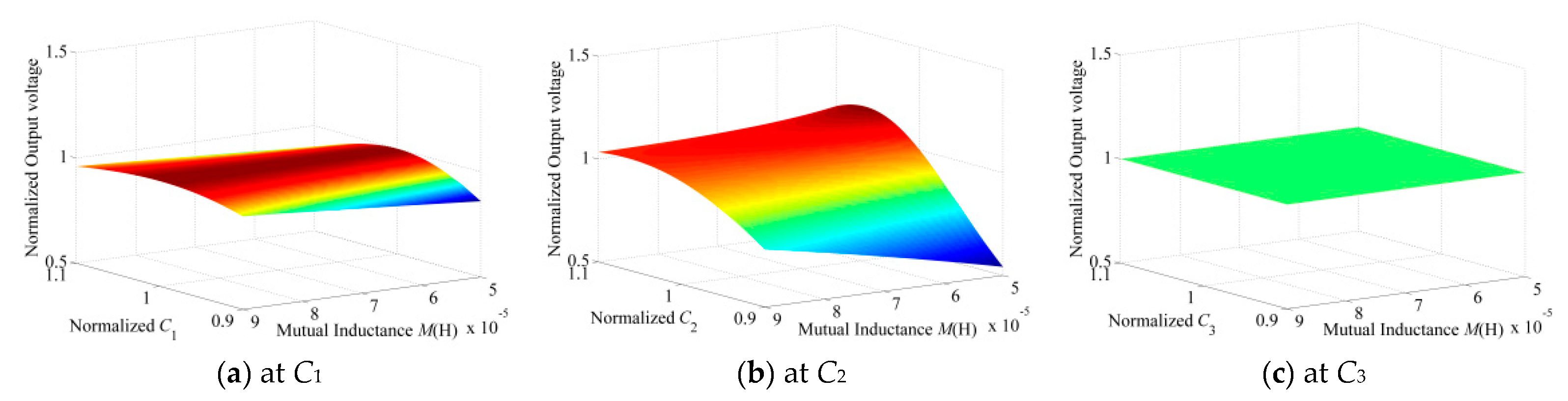
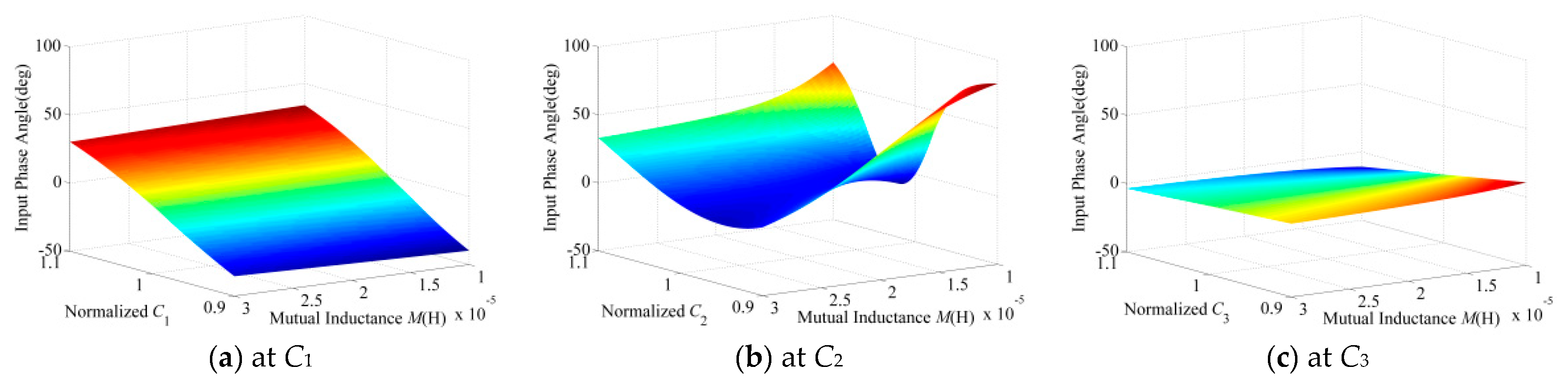
2.2. S-SP Parameter Sensitivity Analysis

In practical applications, the compensation network parameters are inevitably biased, so a sensitivity analysis is needed. The sensitivity of the energy efficiency characteristics is analyzed by using the control variable method. First, it is assumed that the primary compensating capacitor C1 displayed errors while the secondary compensating capacitors C2 and C3 remained unchanged as the reference values.
C 1 E = ( 1 α ) C 1 S C 2 E = C 2 S C 3 E = C 3 S
where C1E, C2E, and C3E are the deviation values after the error coefficient is substituted, and C1S, C2S, and C3S are the reference values when the loosely coupled transformer is not offset, that is, the error coefficient α = 0.
In the same way, a sensitivity analysis is carried out on the influence of the change in the primary and secondary compensation capacitance parameters on the output voltage characteristics and input phase angle characteristics, and the three-dimensional output voltage diagram is drawn when C1, C2, and C3 are affected by the error coefficient, respectively.
Figure 4 presents the variation curve of the normalized output voltage with respect to the compensating capacitance parameter and mutual inductance. From Figure 4a,b, compensating capacitor C1 has a gentle influence on the system output voltage, while compensating capacitor C2 has a greater influence on the system output voltage. Figure 4c indicates that compensation capacitor C3 does not affect the system’s output voltage.
Similarly, the change curve of the input impedance angle with respect to the compensation capacitance parameter and mutual inductance is depicted in Figure 5.
Figure 5a shows that the primary compensated capacitance C1 significantly impacts the system’s impedance angle. As the compensated capacitance C1 increases, the impedance angle also increases and shifts towards the inductive region of the system. From Figure 5b, it can be observed that the input phase angle decreases initially and then increases as the compensated capacitance C2 increases. Figure 5c indicates that the compensated capacitance C3 has minimal influence on the system’s input phase angle. With variations in the C3 parameter, the input phase angle curve exhibits a stable trend.
Through the above analysis, it can be concluded that the change in the secondary compensated capacitance C3 has a slight effect on the output characteristics. Therefore, the secondary compensated capacitance C3 can be replaced by the switching capacitor structure.

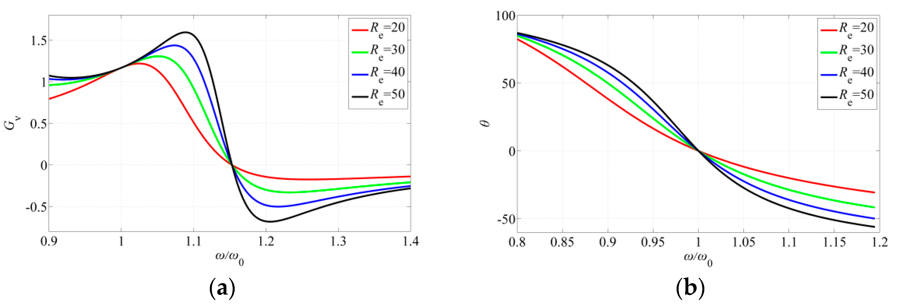
2.3. S-SP Detuned State

When the system is operating in the full resonance state, the S-SP topology can achieve a load-independent voltage output. However, when the coupling coil is offset, the leakage inductance and the excitation inductance change, resulting in the system working in a detuned state. Letting the coupling coefficient be k, the leakage relation can be expressed as L 11 = ( 1 k ) L 1 , L 12 = ( 1 k ) L 2 . Therefore, when the coil does not resonate, the resonant angular frequency can be expressed as follows:
ω 0 = 1 ( 1 k ) L 1 C 1 = 1 ( 1 k ) L 2 C 2
The coupling coil is misaligned, and the coupling coefficient changes. The primary side resonance angular frequency becomes ω1, and the secondary side resonance angular frequency becomes ω2, which can be expressed as follows:
ω 1 = 1 1 k L 1 C 1 = 1 k 1 k ω 0 ω 2 = 1 1 k L 2 C 2 = 1 k 1 k ω 0
At this time, if the frequency modulation control is used to adjust the switching frequency of the inverter to the new resonant angular frequency ω0′, the leakage inductance of the original and secondary side and its corresponding compensation capacitor will be connected in series at the same time, and the leakage inductance will be completely compensated for.
ω 0 = ω 1 = ω 2 = 1 k 1 k ω 0
As for the excitation inductance, the resonant angular frequency under the initial conditions of the system can be expressed as
ω 0 = 1 n 2 k L 1 C 3
When the coupling condition and the coupling coefficient change, the new resonant angular frequency can be expressed as
ω 0 = 1 n 2 k L 1 C 3 = k k ω 0
From (11) and (12), it is clear that ω 0 ω 0 . Clearly, the sensitivity analysis reveals that changes in the compensation capacitor C3 have the least impact on the system’s output characteristics. A variable capacitor can be employed at the secondary side to re-establish resonance when the coupling coil experiences misalignment.

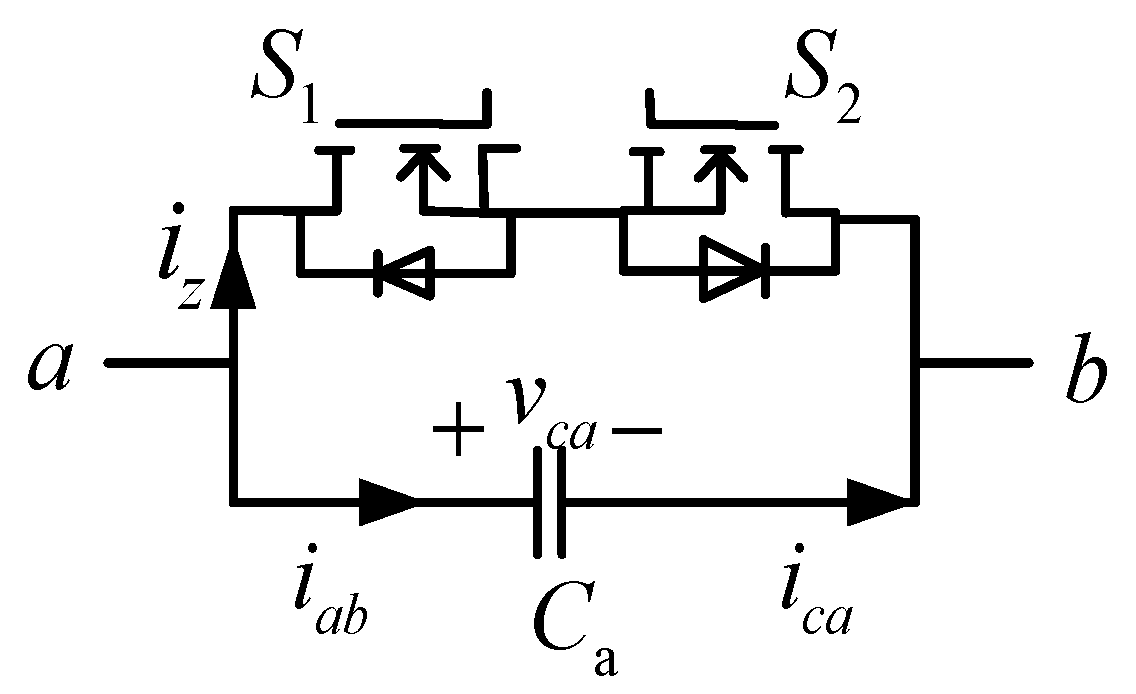
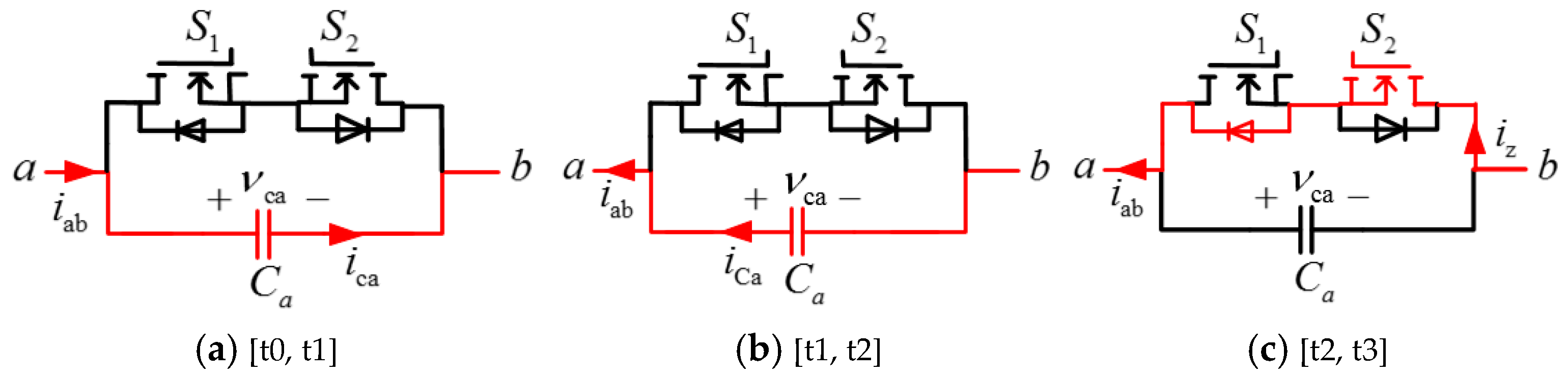
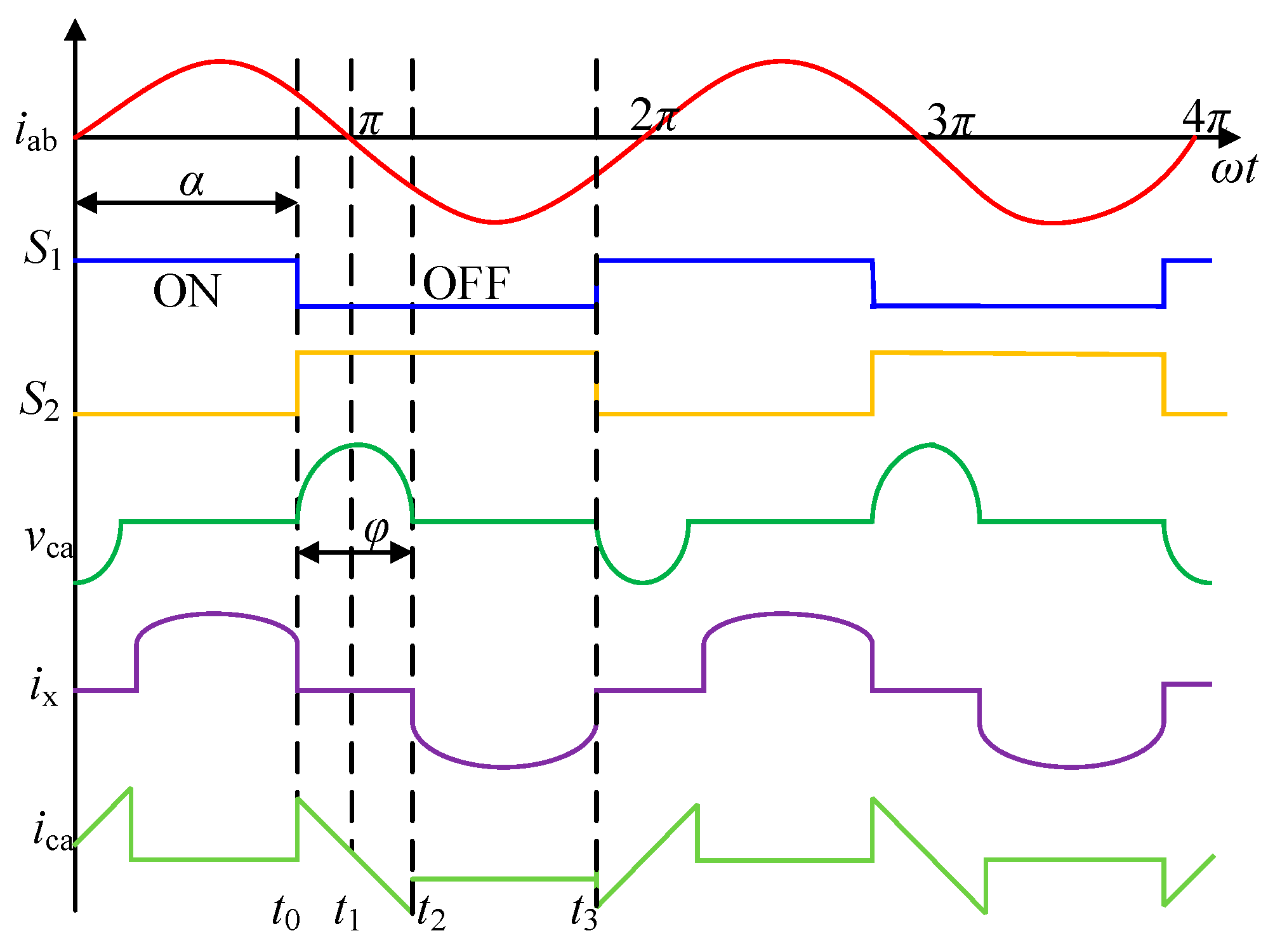
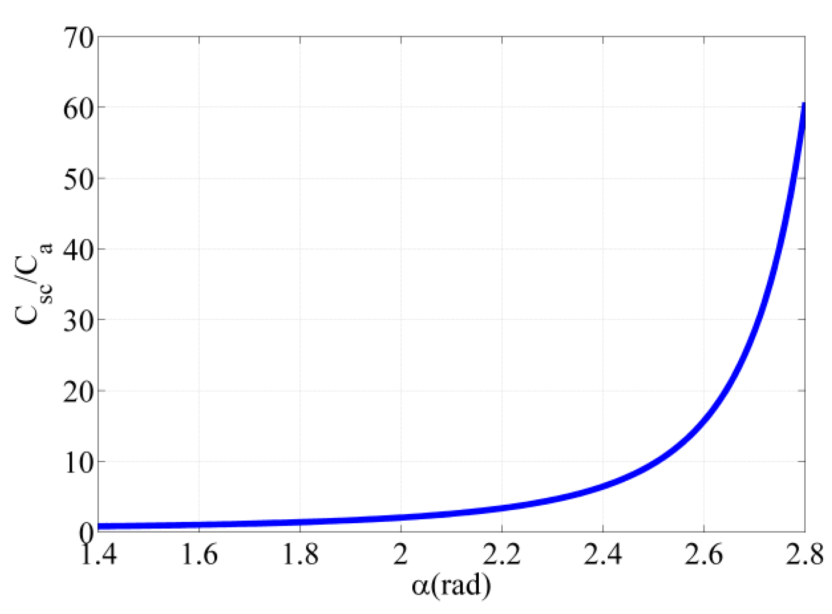
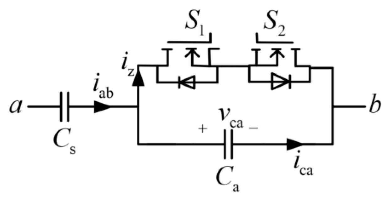
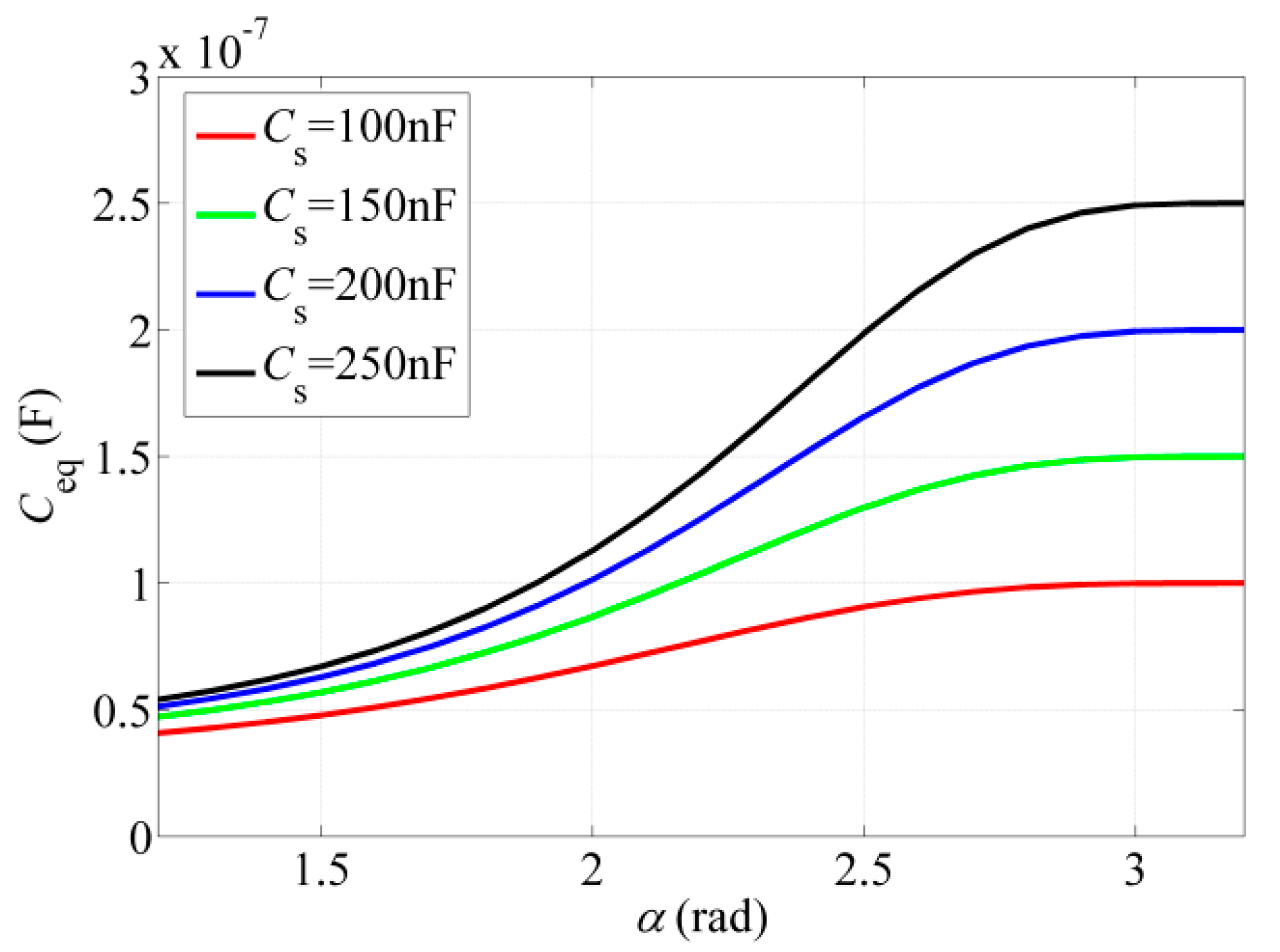
3. Principle Analysis of SCC Strategy

The topology of the switched capacitor is shown in Figure 6, consisting of a group of anti-series connected switch tubes S1 and S2 in parallel with a fixed capacitor Ca. By controlling the conduction angle α of the two switch tubes S1 and S2, the waveform of the current passing through the fixed capacitor Ca is changed, thereby controlling the equivalent capacitance value. The operating mode of the switching capacitors is shown in Figure 7 and Figure 8.
State 1 [t0, t1]: The drive signal for switch tube S1 disappears, and the current can only flow forward through the fixed capacitor Ca. During this period, iab = ica, iz = 0, and the voltage across the capacitor vca rises until the moment t1 when the current iab crosses zero, triggering the drive signal for switch tube S2.
State 2 [t1, t2]: At the moment t1 when the current iab crosses zero, the drive signal for switch tube S2 is triggered. However, due to the clamping effect of the capacitor voltage vca, switch tube S2 cannot conduct, and the current iab can only discharge in reverse through the fixed capacitor Ca. During this period, iab = ica, iz = 0, and the voltage across the capacitor vca decreases until vca = 0.
State 3 [t2, t3]: At the moment t2 when the capacitor voltage vca = 0, and the drive signal for switch tube S2 remains high, the current iab will flow through the parasitic diodes of the switch tube S2 itself and S1. During this period, iab = iz, ica = 0, vca = 0, and the voltage across the switch tube S2 is 0 when it turns on, achieving zero-voltage turn-on. Until the moment t3, when the drive signal for switch tube S2 disappears, the voltage across S2 remains 0 when it turns off, achieving zero-voltage turn-off.
The half-cycle process after the moment t3 is similar to the above process and will not be detailed. From the above analysis, it can be seen that the switching tubes S1 and S2 in the switching capacitance topology achieve soft switching, and adopting this topology will not increase the switching loss of the system.
Thus, within the interval [α, α + φ], the capacitor voltage vca is given by
ν ca = 1 C a α / ω t I ab sin ω t d t = I ab ω C a [ cos α cos ω t ]
When ωt = α + φ, we have vca = 0. Therefore, the relationship α = π − φ/2 can be obtained.
According to (13), the fundamental component vca1 of the capacitor voltage can be obtained as
ν ca 1 = 2 π α α + φ ν ca cos ( ω t ) d ω t = I ab ω [ ( π α + 1 2 sin 2 α ) 2 π C a ]
From C sc = i ab 1 / j ω v ca 1 , the relation between the equivalent capacitance of the switching capacitor Csc and the conduction angle α is
C sc = C a 2 2 α sin 2 α / π
From (15), the curve of Csc/Ca and the conduction angle α is plotted as shown in Figure 9, where the conduction angle α varies within the range [π/2, π], corresponding to the adjustable range of the equivalent capacitance value [Ca, +∞].
Figure 9 illustrates that the equivalent capacitance value Csc of the switching capacitor monotonically increases with the increase in angle α. The equivalent capacitance of the switching capacitor is achieved when α = π/2. In this case, the sinusoidal current iab will continue to flow through the capacitor Ca. Although there are driving signals in switching tubes S1 and S2, they are always in the off state under the clamping action of capacitive voltage vca. When α = π, the two switching tubes will be complementary, the sinusoidal current iab will flow through the two switching tubes, and the fixed capacitance Ca will be equivalent to a short circuit, so the equivalent capacitance of the switching capacitor Csc will be equivalent to infinity. This is very unfavorable for controlling the switching capacitance, because a small on-angle α deviation will cause a large equivalent capacitance value Csc, thus affecting the control performance. To enhance the precision of the switched capacitor control, a fixed capacitor Cs can be connected in series ahead of the switched capacitor topology. The circuit topology for this configuration is depicted in Figure 10.
After connecting the fixed capacitor Cs in series, the expression for the equivalent capacitance value is given by
C eq = C sc C s C sc + C s = π C a C s π C a + C s 2 π 2 α + sin 2 α
According to Equation (16), the equivalent capacitance Ceq curve with a different angle α is drawn in Figure 11. It is assumed that Ca = 50 nF and Cs = 100 nF, 150 nF, 200 nF, and 250 nF, respectively.
When the conducting angle α > 0.95π, the equivalent capacitance Ceq remains basically unchanged, so this section needs to be omitted, and a certain margin needs to be retained during use in reality. In this paper, the maximum equivalent capacitance value Cmax is obtained when the conduction angle α = 0.9π. Similarly, because the relation curve is too gentle when the conduction angle α < 0.5π, this section should also be omitted, and the minimum value Cmin for the equivalent capacitance can be achieved when the conduction angle α=0.55π after the margin is retained.
Therefore, by adjusting the conduction angle α, the equivalent capacitance can be changed, thereby tuning the resonance of the system. This ensures that the parallel resonance returns to its value at the new resonant frequency. A tuning control strategy based on the switched capacitor is proposed, which is illustrated in Figure 12. The process begins by setting the conduction angle α of the switched capacitor circuit, calculating the input phase angle θ, and then adjusting the conduction angle of the switched capacitor circuit according to the specified tuning strategy. (1) If θ is less than 0, indicating a capacitive state, the conduction angle α should be reduced. (2) If θ is greater than 0, indicating an inductive state, the conduction angle α should be increased. (3) When the input phase angle θ is equal to 0, the input impedance exhibits a pure resistive state. The system achieves complete resonance, and a unity power factor is achieved. In the actual tuning process, the adjustment step size Δα of the conduction angle can be set according to the practical needs. If the step size Δα is set too large, the control accuracy cannot be guaranteed. If the step size Δα is set too small, it will increase the system overhead time, and the tuning time will be too long. Therefore, the step size Δα should be set appropriately. The control strategy adjusts the conduction angle in increments according to a predetermined step size. Ultimately, it modifies the output impedance angle of the system’s transmitting end to zero, thereby restoring the system to its resonant working state.

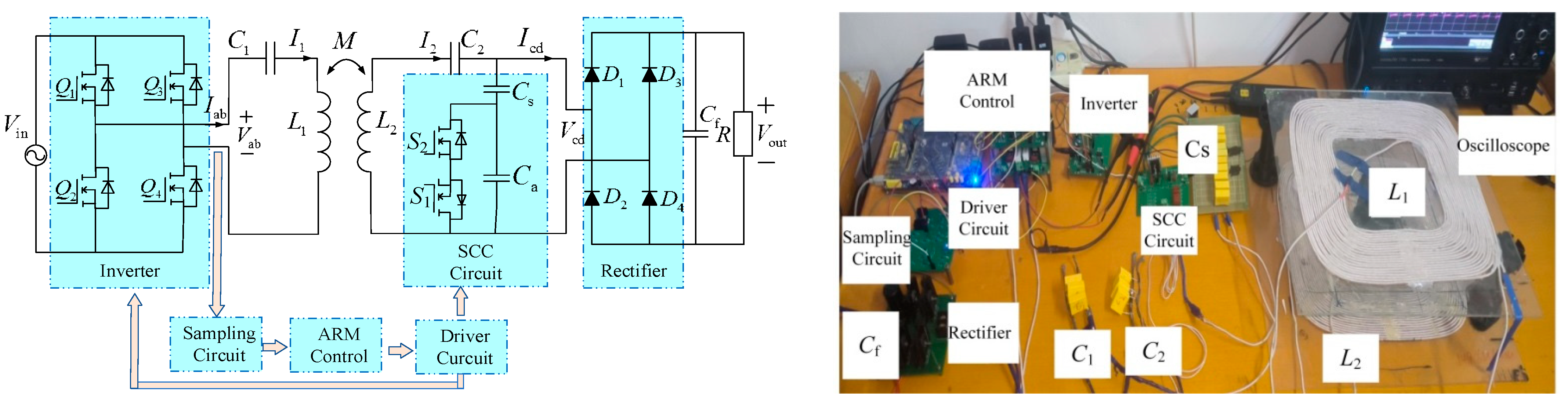
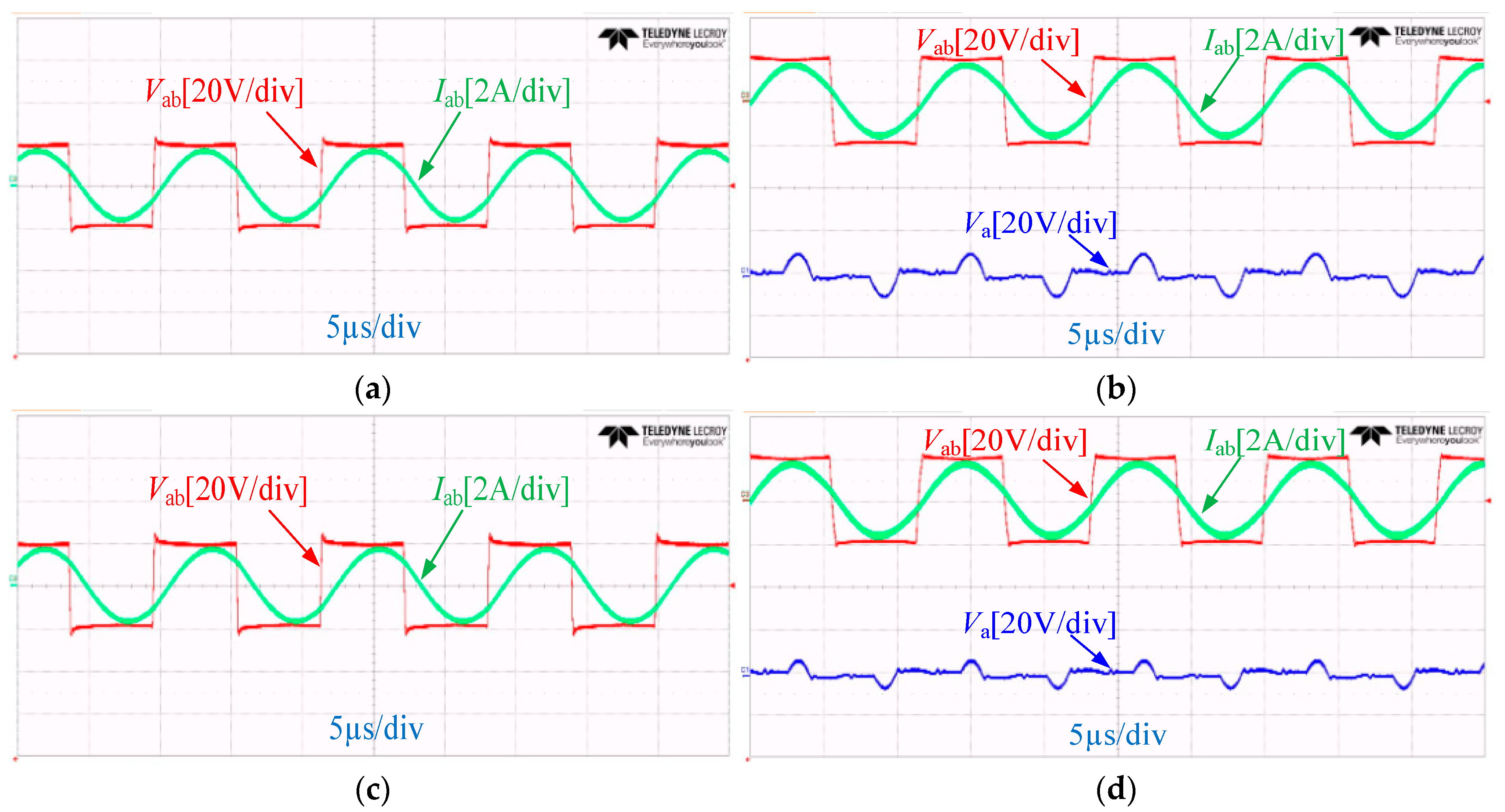
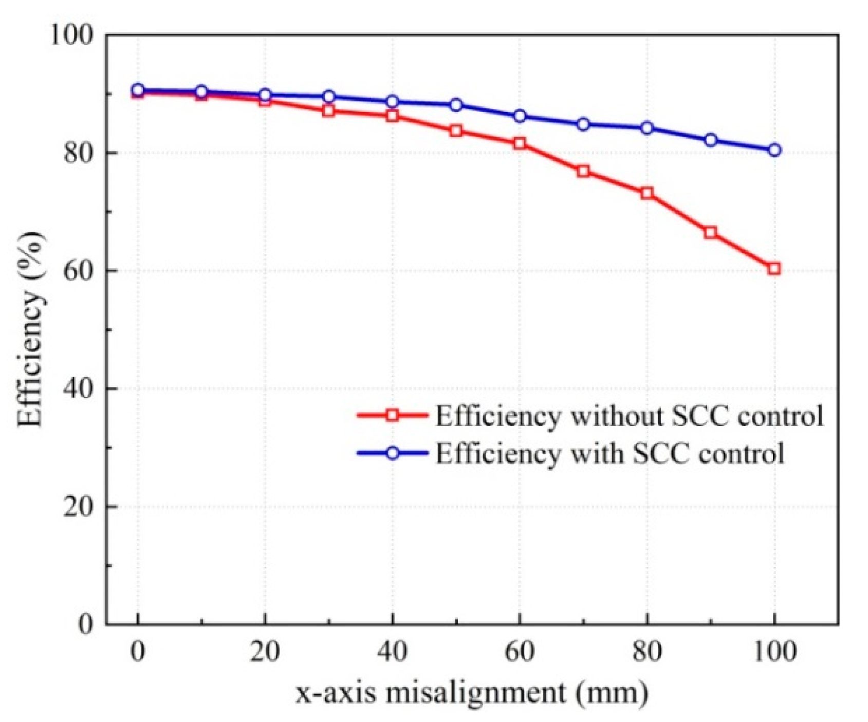
4. Experimental Verification

To validate the practicality of the proposed IPT system, a prototype experimental setup was constructed as shown in Figure 13. In the system, the PWM duty cycle of the high-frequency inverter is maintained at 50%. The initial operating frequency is set to 85 kHz. The MOSFET Q1–Q4 in the full-bridge inverter unit is IRFP460PBF, and the diodes D1–D4 in the rectifier are IDW40G120C5B. The size of the coupling pad is 300 mm × 300 mm × 100 mm. The specific parameters of the system are detailed in Table 1.
Figure 14 shows the experimental waveforms under the x-axis misalignment of the S-SP topology IPT system, where Vab, Iab, and Va represent the inverter output voltage, the inverter output current, and the switching capacitance output voltage, respectively. Figure 14a,c demonstrate that, as the offset distance increases, the phase difference between the output voltage and current of the inverter also increases. This indicates that an increase in the reactive power will lead to a decrease in the system’s output efficiency. When the S-SP topology IPT system employs SCC control, the phase difference between the output voltage and current of the inverter is nearly zero, suggesting improved efficiency.
Figure 15 shows the experimental waveforms under z-axis misalignment. As is shown, the S-SP topology IPT system with SCC control can also achieve a zero phase angle under z-axis misalignment. As the offset distance of the system’s coupling coil increases, the time at which Vca = 0 becomes longer, and the turn-on angle of the corresponding switching capacitor increases, indicating that the equivalent capacitance of the switching capacitor increases accordingly, which is consistent with the theoretical analysis.
Figure 16 shows the experimental waveforms under different loads and misalignments. It is clear from Figure 16a that the proposed S-SP topology IPT system can achieve almost constant voltage. When there is a sudden misalignment change, the dynamic adjustment time is about 0.8 s, as shown in Figure 16b. Moreover, the proposed S-SP topology IPT system with SCC control can maintain a stable output voltage, which indicates that the system has good misalignment tolerance.
The system efficiency under different x-axis misalignments is depicted in Figure 17. When the x-axis misalignment increases from 0mm to 100mm, the coupling coefficient drops from 0.224 to 0.145. It is obvious that the system efficiency without SCC control varies from 90% to 60%, while the system efficiency with SCC control varies from 90% to 80%. It is evident that the proposed S-SP topology with SCC control can improve the system efficiency under misalignment conditions.
In order to achieve misalignment tolerance without wireless communication and control schemes, parameter optimization is designed to realize a constant output power. Particle swarm optimization (PSO) is proposed to obtain a constant voltage in [25], and this comprises four components, as shown in Table 2. However, this design process is relatively complex. In order to reduce the components, a detuned SS-compensated topology is presented in [26], which only contains two components. The proposed detuned SS topology can also provide constant power at the expense of efficiency. An S-SP-compensated topology is proposed in [27] that can maintain a steady output voltage. Compared with [25] and [28], the proposed IPT system uses fewer components, which can reduce the volume and cost. In references [25,26,27], the proposed IPT system with SCC control can achieve a zero phase angle (ZPA), which can help to increase the system efficiency. Compared with the system presented in [28], the IPT system proposed here can also achieve a constant voltage with misalignment tolerance.

5. Conclusions

In this article, an S-SP-compensated inductive power transfer (IPT) system with a high misalignment tolerance based on a switch-controlled capacitor is proposed. A mathematical model for the S-SP compensation network is developed, enabling a load-independent output voltage. A sensitivity analysis of the compensation element parameters is conducted, revealing that the secondary compensated capacitor C3 has a slight effect on both the output voltage and input impedance. Additionally, an improved switching capacitor structure is introduced to dynamically compensate for changes in the S-SP IPT system. An experimental prototype was constructed to validate the theoretical analysis, confirming its correctness and feasibility. The experimental results demonstrate that the proposed method ensures the system operates in a resonant state with high efficiency, even when the coupling pad experiences up to 30% horizontal misalignment (with the coupling coefficient varying from 0.22 to 0.14). In addition, the proposed SCC structure is not limited to S-SP topologies, and can be used for other topologies such as LCC-S, S-LCC, and LCC-LCC. A 3.7 kW electric vehicle wireless charging system will be built according to SAE 2954.

Author Contributions

Conceptualization, H.W. and Z.G.; formal analysis, Y.Y.; funding acquisition, N.Z.; investigation, Z.G.; methodology, H.Z. and Z.G.; project administration, N.Z.; software, M.X. and Hao Wang; visualization, N.Z.; writing—original draft, Z.G.; writing—review and editing, Z.G. All authors have read and agreed to the published version of the manuscript.

Funding

This research was funded by Shaanxi Province Qin Chuangyuan Scientist & Engineer Project under Grant 2023KXJ-151; Xi’an Qin Chuangyuan Scientist + Engineer Project under Grant 23KGDW0015-2023; Shaanxi Innovation Ability Support Plan under Grant 2024RS-CXTD-13.

Data Availability Statement

Data are contained within the article.

Conflicts of Interest

The authors declare no conflicts of interest.

References

  1. Cui, J.; Wei, G.; Wang, Y. A Novel Impedance Compensation Method for IPT System Applying Inverse Coupled Current Doubler Rectifier. IEEE Trans. Power Electron. 2024, 71, 15235–15238. [Google Scholar] [CrossRef]
  2. Tao, C.; Liu, Z.; Li, S.; Guo, Y.; Wang, L. A High-efficiency Wireless Power Transfer System Using Quasi-Z-Source Inverter and Current-Double Synchronous Rectifier for Low-Voltage and High-Current Applications. IEEE Trans. Transp. Electrif. 2022, 8, 2758–2769. [Google Scholar] [CrossRef]
  3. Jeong, M.S.; Jang, J.H.; Lee, E.S. Optimal IPT Core Design for Wireless Electric Vehicles by Reinforcement Learning. IEEE Trans. Power Electron. 2023, 38, 13262–13272. [Google Scholar] [CrossRef]
  4. Zhang, X.; Xue, R.; Wang, F.; Xu, F.; Chen, T.; Chen, Z. Capacitor Tuning of LCC-LCC Compensated IPT System with Constant-Power Output and Large Misalignments Tolerance for Electric Vehicles. IEEE Trans. Power Electron. 2023, 38, 11928–11939. [Google Scholar] [CrossRef]
  5. Feng, H.; Dayerizadeh, A.; Lukic, S. A Coupling-Insensitive X-Type IPT System for High Position Tolerance. IEEE Trans. Ind. Electron. 2021, 68, 6917–6926. [Google Scholar] [CrossRef]
  6. Li, H.; Liu, Y.; Zhou, K.; He, Z.; Li, W.; Mai, R. Uniform Power IPT System with Three-Phase Transmitter and Bipolar Receiver for Dynamic Charging. IEEE Trans. Power Electron. 2019, 34, 2013–2017. [Google Scholar] [CrossRef]
  7. Lu, J.; Zhu, G.; Lin, D. Load-Independent Voltage and Current Transfer Characteristics of High-Order Resonant Network in IPT System. IEEE J. Emerg. Sel. Top. Power Electron. 2019, 7, 422–436. [Google Scholar] [CrossRef]
  8. Dai, X.; Li, X.; Li, Y.; Hu, A.P. Maximum Efficiency Tracking for Wireless Power Transfer Systems with Dynamic Coupling Coefficient Estimation. IEEE Trans. Power Electron. 2018, 33, 5005–5015. [Google Scholar] [CrossRef]
  9. Yang, L.; Shi, Y.; Wang, M.; Ren, L. Constant Voltage Charging and Maximum Efficiency Tracking for WPT Systems Employing Dual-Side Control Scheme. IEEE J. Emerg. Sel. Top. Power Electron. 2022, 10, 945–955. [Google Scholar] [CrossRef]
  10. Yao, Y.; Wang, Y.; Liu, X. Analysis, Design, and Optimization of LC/S Compensation Topology with Excellent Load-Independent Voltage Output for Inductive Power Transfer. IEEE Trans. Transp. Electrif. 2018, 4, 767–777. [Google Scholar] [CrossRef]
  11. Wang, C.; Covic, G.; Stielau, O. Power transfer capability and bifurcation phenomena of loosely coupled inductive power transfer systems. IEEE Trans. Ind. Electron. 2004, 51, 148–157. [Google Scholar] [CrossRef]
  12. Li, Z.; Song, K.; Jiang, J.; Zhu, C. Constant Current Charging and Maximum Efficiency Tracking Control Scheme for Supercapacitor. IEEE Trans. Power Electron. 2022, 33, 9088–9100. [Google Scholar] [CrossRef]
  13. Zhang, X.; Liu, F.; Mei, T. Multifrequency Phase-Shifted Control for Multiphase Multiload MCR WPT System to Achieve Targeted Power Distribution and High Misalignment Tolerance. IEEE Trans. Power Electron. 2021, 36, 991–1003. [Google Scholar] [CrossRef]
  14. Miller, J.; Onar, O.; Chinthavali, M. Primary-side power flow control of wireless power transfer for electric vehicle charging. IEEE J. Emerg. Sel. Top. Power Electron. 2015, 3, 147–162. [Google Scholar] [CrossRef]
  15. Zhang, Z.; Zhang, B. Angular-Misalignment Insensitive Omnidirectional Wireless Power Transfer. IEEE Trans. Ind. Electron. 2020, 67, 2755–2764. [Google Scholar] [CrossRef]
  16. Kim, S.; Covic, G.; Boys, J. Tripolar Pad for Inductive Power Transfer Systems for EV Charging. IEEE Trans. Power Electron. 2017, 32, 5045–5057. [Google Scholar] [CrossRef]
  17. Chen, Y.; Yang, B.; Zhou, X.; Li, Q.; He, Z.; Mai, R.; Lai, J.S. A Hybrid Inductive Power Transfer System with Misalignment Tolerance Using Quadruple-D Quadrature Pads. IEEE Trans. Ind. Electron. 2020, 35, 6039–6049. [Google Scholar] [CrossRef]
  18. Yao, Y.; Wang, Y.; Liu, X.; Pei, Y. A Novel Unsymmetrical Coupling Structure Based on Concentrated Magnetic Flux for High-Misalignment IPT Applications. IEEE Trans. Power Electron. 2019, 34, 3110–3123. [Google Scholar] [CrossRef]
  19. Ahmad, A.; Alam, M.S.; Mohamed, A.A.S. Design and Interoperability Analysis of Quadruple Pad Structure for Electric Vehicle Wireless Charging Application. IEEE Trans. Transp. Electrif. 2019, 5, 934–945. [Google Scholar] [CrossRef]
  20. Zhao, L.; Thrimawithana, D.; Madawala, U. Hybrid Bidirectional Wireless EV Charging System Tolerant to Pad Misalignment. IEEE Trans. Ind. Electron. 2017, 64, 7079–7086. [Google Scholar] [CrossRef]
  21. Zhao, L.; Thrimawithana, D.J.; Madawala, U.K.; Hu, A.P.; Mi, C.C. A Misalignment-Tolerant Series-Hybrid Wireless EV Charging System with Integrated Magnetics. IEEE Trans. Power Electron. 2019, 34, 1276–1285. [Google Scholar] [CrossRef]
  22. Qu, X.; Yao, Y.; Wang, D.; Wong, S.C.; Chi, K.T. A Family of Hybrid IPT Topologies with Near Load-Independent Output and High Tolerance to Pad Misalignment. IEEE Trans. Ind. Electron. 2020, 35, 6867–6877. [Google Scholar] [CrossRef]
  23. Mai, J.; Wang, Y.; Yao, Y.; Xu, D. Analysis and Design of High-Misalignment-Tolerant Compensation Topologies with Constant-Current or Constant-Voltage Output for IPT Systems. IEEE Trans. Power Electron. 2021, 36, 2685–2695. [Google Scholar] [CrossRef]
  24. Yang, B.; Li, Y.; Zhang, Z.; He, S.; Peng, Y.; Chen, Y.; He, Z.; Mai, R. A Detuned S-S Compensated IPT System with Two Discrete Frequencies for Maintaining Stable Power Transfer Versus Wide Coupling Variation. IEEE Trans. Transp. Electrif. 2023, 9, 3836–3848. [Google Scholar] [CrossRef]
  25. Yao, Y.; Wang, Y.; Liu, X.; Pei, Y.; Xu, D.; Liu, X. Particle Swarm Optimization-Based Parameter Design Method for S/CLC-Compensated IPT Systems Featuring High Tolerance to Misalignment and Load Variation. IEEE Trans. Power Electron. 2019, 34, 5268–5282. [Google Scholar] [CrossRef]
  26. Feng, H.; Cai, T.; Duan, S.; Zhang, X.; Hu, H.; Niu, J. A Dual-Side-Detuned Series–Series Compensated Resonant Converter for Wide Charging Region in a Wireless Power Transfer System. IEEE Trans. Ind. Electron. 2018, 65, 2177–2188. [Google Scholar] [CrossRef]
  27. Wang, Y.; Mai, J.; Yao, Y.; Xu, D. Analysis and Design of an IPT System Based on S/SP Compensation with Improved Output Voltage Regulation. IEEE Trans. Ind. Inform. 2020, 16, 3256–3266. [Google Scholar] [CrossRef]
  28. Zhou, L.; Mai, R.; Liu, S.; Yu, J.; Li, Y.; Fu, L. Minimizing Input Current of the Rectifier of LCC–LCC Compensated IPT Systems by Switch-Controlled Capacitor for Improving Efficiency. IEEE Trans. Ind. Appl. 2022, 58, 1010–1021. [Google Scholar] [CrossRef]
Figure 1. IPT system with S-SP compensation topology.
Electronics 14 00188 g001
Figure 2. The equivalent S-SP compensation topology.
Electronics 14 00188 g002
Figure 3. The output voltage gain and input phase angle curves of S-SP compensation topology. (a) S-SP compensation topology output voltage gain. (b) S-SP compensation topology input phase angle.
Electronics 14 00188 g003
Figure 4. The output voltage sensitivity.
Electronics 14 00188 g004
Figure 5. The input phase angle sensitivity.
Electronics 14 00188 g005
Figure 6. Switching capacitor topology.
Electronics 14 00188 g006
Figure 7. Operating mode of switching capacitors.
Electronics 14 00188 g007
Figure 8. Sequence diagram of switching capacitor operation.
Electronics 14 00188 g008
Figure 9. The equivalent capacitance value of the switching capacitor.
Electronics 14 00188 g009
Figure 10. Improved switching capacitor structure.
Electronics 14 00188 g010
Figure 11. Equivalent capacitance value Ceq curve with different angle α.
Electronics 14 00188 g011
Figure 12. Flow chart of switching capacitor control method.
Electronics 14 00188 g012
Figure 13. Experimental setup of the proposed IPT system.
Electronics 14 00188 g013
Figure 14. Experimental waveforms of the inverter and switching capacitance under x-axis misalignment. (a) Under 40 mm x-axis misalignment without SCC. (b) Under 40 mm x-axis misalignment with SCC. (c) Under 100 mm x-axis misalignment without SCC. (d) Under 100 mm x-axis misalignment with SCC.
Electronics 14 00188 g014
Figure 15. Experimental waveforms of the inverter and switching capacitance at z-axis misalignment. (a) Under 30 mm z-axis misalignment without SCC. (b) Under 30 mm z-axis misalignment with SCC. (c) Under 50 mm z-axis misalignment without SCC. (d) Under 50 mm z-axis misalignment with SCC.
Electronics 14 00188 g015
Figure 16. Experimental waveforms of the inverter and load under different loads and misalignments.
Electronics 14 00188 g016
Figure 17. System efficiency under different x-axis misalignments.
Electronics 14 00188 g017
Table 1. Parameter values of the S-SP IPT system.
ParameterValueParameterValue
Uin20/Vf85/kHz
L1149.56/μHCs250/nF
L2149.2/μHCa50/nF
Lf470/μHCf50/nF
C130/nFM34.5/uH
C230/nFR20/30/Ω
Table 2. Comparison with related works with misalignment tolerance.
Proposed in[25][26][27][28]This Work
Compensation topologyS-CLCSSS-SPLCC-LCCS-SP
Number of components42363
Coupling coefficient0.2–0.40.08–0.20.14–0.2850.128–0.1730.14–0.2
Output characteristicConstant
Voltage
Constant
Power
Constant
Voltage
Constant
Current
Constant
Voltage
Misalignment toleranceYesYesYesNoYes
Input phase angleZVSZVSZVSZPAZPA
Disclaimer/Publisher’s Note: The statements, opinions and data contained in all publications are solely those of the individual author(s) and contributor(s) and not of MDPI and/or the editor(s). MDPI and/or the editor(s) disclaim responsibility for any injury to people or property resulting from any ideas, methods, instructions or products referred to in the content.

