Article

An Energy-Efficient 12-Bit VCO-Based Incremental Zoom ADC with Fast Phase-Alignment Scheme for Multi-Channel Biomedical Applications

College of Engineering, Electrical, and Electronics Engineering, Pusan National University, Busan 46241, Republic of Korea
*
Author to whom correspondence should be addressed.
Electronics 2024, 13(9), 1754; https://doi.org/10.3390/electronics13091754
Submission received: 5 April 2024 / Revised: 27 April 2024 / Accepted: 30 April 2024 / Published: 2 May 2024

Abstract

:
This paper presents a low-power, energy-efficient, 12-bit incremental zoom analog-to-digital converter (ADC) for multi-channel bio-signal acquisitions. The ADC consists of a 7-stage ring voltage-controlled oscillator (VCO)-based incremental ΔΣ modulator (I-ΔΣM) and an 8-bit successive approximation register (SAR) ADC. The proposed VCO-based I-ΔΣM can provide fast phase-alignment of the ring-VCO to reduce the interval settling time; thereby, the I-ΔΣM can accommodate time-division-multiplexed input signals without phase leakage between consecutive measurements. The SAR ADC also adopts splitting unit capacitors that can support VCM-free tri-level switching and prevent invalid states from the phase frequency detector with minimal logic gates and switches. The proposed ADC has been fabricated in a standard 180 nm standard 1P6M CMOS process, exhibiting a 67-dB peak signal-to-noise ratio, a 74-dB dynamic range, and a Walden figure of merit of 19.12 fJ/c-s, while consuming a power of 3.51 μW with a sampling rate of 100 kS/s.

1. Introduction

Over the past few decades, there has been a growing research interest in low-power circuit designs for battery-powered sensing devices for portable, wearable, or implantable biomedical applications [1,2,3,4,5]. These devices for biomedical applications are usually used to detect and monitor neural signals such as electrocardiogram (ECG), electroencephalogram (EEG), electromyogram (EMG), local field and action potentials, and other bio-signals like body temperature and impedance, and epidermal activity (EDA). Most bio-signals are characterized by small amplitude but relatively large dynamic range [6,7]. Thus, frontend circuits are typically composed of low-noise amplifiers and filters for signal pre-conditioning, followed by analog-to-digital converters (ADCs) for digital signal processing (DSP) [8,9,10,11,12]. Of these components, the ADCs are known to be one of the most power-hungry blocks due to relatively high dynamic range (>11-bit) and wide sampling rate (>1–30 kS/s) requirements for high integrity of the signals.
Successive approximation register (SAR) ADCs have long been recognized as a strong candidate for such low-power ADC design because of their zero static power consumption [13,14]. In addition, recent research on advanced switching techniques in SAR ADCs has reinforced the high energy efficiency of the SAR ADCs [15]. However, to achieve a high resolution in SAR ADCs (>11-bit), they should be equipped with pre-amplification before bit decision, which often requires calibration and correction techniques, consequently resulting in higher power consumption overhead. Recently, hybrid ADCs, where different types of ADC are combined, have been proposed to complementarily achieve low-power and high-resolution performance. Among them, an incremental zoom ADC, which merges SAR ADC with high power efficiency and incremental delta-sigma modulator (I-ΔΣM) with high accuracy, has the advantage of high energy efficiency [16].
An I-ΔΣM typically consists of an analog filter, quantizer, and a digital-to-analog converter (DAC). The analog filter requires an operational transconductance amplifier (OTA), which is one of the most power-hungry circuit blocks for converting small residual voltages by coarse feedback to digital outputs. In recent years, the ΔΣ operation assisted by a VCO-based quantization in the time domain has been researched [17,18,19,20,21]. Since the VCO can be regarded as an integrator in the time domain, it acts as an integrator when embedded in the ΔΣ loop and viewed from a different time axis [17]. Thus, constructing a ΔΣ loop with ring-VCOs can replace the power-hungry OTAs, and the inner ADC on the time domain can be designed at the semi-digital level, favoring the advanced CMOS technologies.
However, there is a limitation when using it in I-ΔΣM for multi-channel signal acquisitions. Unlike ΔΣM dedicated to a single channel measurement where VCO-based quantizers do not explicitly reset the integrator (VCO) [22], I-ΔΣM for multichannel data acquisition needs to periodically reset the history of data for processing new samples without errors [23]. Otherwise, dynamic phase offset leaks into the consecutive conversion, resulting in performance degradation. Particularly for the incremental mode with limited oversampling ratio (OSR), i.e., for low cycles, the resolution of I-ΔΣ ADC can be further negatively affected due to such voltage-referred phase offset.
In this article, we propose a zoom ADC combining an SAR ADC and a VCO-based I-ΔΣM with a simple and fast phase-alignment scheme, so that it can be used for multi-channel bio-signal acquisitions without power and area overheads. To further reduce area and power consumptions, we adopt the VCM-free splitting unit capacitors [24] for the SAR ADC while using the merged capacitor switching (MCS) scheme [14]. The tri-level capacitive feedback scheme has also been adopted to eliminate error states caused by low voltage logics with minimal switches. For better matching between the SAR and the I-ΔΣ, we merged the capacitor digital-to-analog converter (CDAC) and shared the transconductance (Gm) stage. The fabricated ADC performs a low power of 3.6 μW at a 100 kS/s sampling rate for 12-bit resolution. This paper is organized as follows: Section 2 briefly describes the overall proposed incremental zoom ADC architecture. Section 3 represents overall circuit implementations. The measurement results are presented in Section 4. Finally, Section 5 provides the conclusions.

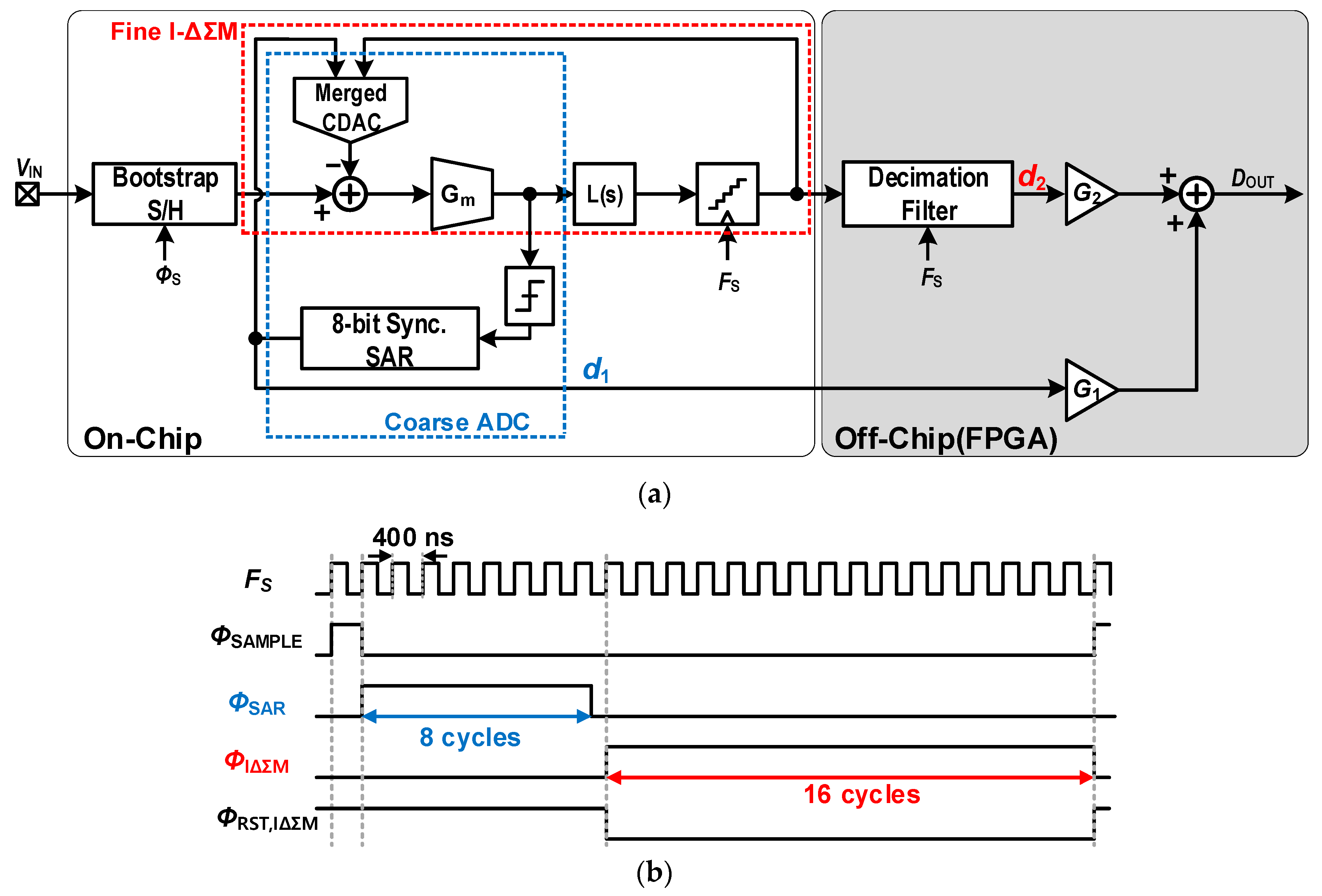
2. Zoom ADC Architecture

2.1. Coarse and Fine Operation

Figure 1a shows the overall architecture of the proposed zoom ADC, consisting of an 8-bit SAR ADC and a 1st order I-ΔΣM as coarse and fine converters, respectively. The input voltage (VIN) is sampled by the CDAC via a pair of bootstrap sample-and-hold (S/H) circuits, and the sampled input is converted to d1 by the SAR operation. The residual voltage is generated by feeding back the corresponding value of d1. The remaining small residual voltage is then processed to d2 by the I-ΔΣM and the decimation filter, and these two digital values are added through the off-chip FPGA with the respective gains of G1 and G2 to get DOUT of the ADC. The final code, DOUT, can be calculated according to (1)
D OUT = G 1 d 1 + G 2 d 2 G 1 = C SAR C SAR + C I Δ Σ + C P , G 2 = C Ι Δ Σ C SAR + C I Δ Σ + C P
where CSAR, CIΔΣ, and CP are the total capacitance assigned for the SAR, ΔΣ operations, and parasitic capacitance, respectively. Increasing the resolution of the SAR ADC increases the energy efficiency and, conversely, increases the impact of the CDAC mismatch and increases the power consumption of the comparator. Since the noise of the comparator is compensated by the fine converter in the zoom ADC architecture, it is necessary to consider the mismatch of the CDAC to improve energy efficiency. In this work, the 8-bit SAR with the MCS scheme was chosen to provide higher energy efficiency because the mismatch (<0.5%) in unit capacitance ensures linearity over 12-bit. Additionally, the 8-bit CDAC produces a low residual voltage, which mitigates the nonlinearity issues of VCO-based ADCs.
In this work, the two ADCs that are combined to form the presented ADC are designed as follows: the 8-bit synchronous SAR is designed to reduce the complexity of the reference voltage buffer and to employ the MCS technique, which is tri-level switching; the I-ΔΣM is presented with a 7-stage ring voltage-controlled-oscillator (VCO)-based loop filter and time-splitting multi-bit quantizer to maximize energy efficiency with the proposed phase-synchronization scheme. The timing diagram for the operation of the proposed ADC is shown in Figure 1b. The main clock (FS) runs at 2.5 MHz and consists of a total of 25 cycles for one sample. The input voltage of the ADC is sampled into the merged CDAC using the top-plate sampling for the first cycle, indicated as ΦSAMPLE. The 8-bit synchronous SAR starts conversion on the falling of ΦSAMPLE and outputs the corresponding digital outputs through the binary search for a total of eight cycles (ΦSAR) and feeds back the information about the value to build up a residual voltage for fine conversion. Finally, the I-ΔΣM performs a fine conversion of the residual voltage with an oversampling ratio of 16 for the rest of the cycles. The merged CDAC consists of total of 519-unit capacitors (512- and 7-unit capacitors are allocated for SAR operation and for the feedback operation of the I-ΔΣM, respectively). Since the two groups of unit capacitors have exactly the same structure and share their top plates, the gain function of G1 and G2 are greatly simplified: G1/G2 = 7/512. In addition, the unit capacitor is split into two parallel-connected half-size capacitors of 4-fF to easily perform tri-level DAC operation. This is covered in more detail in Section 3. The total capacitance of the merged CDAC is 4.152-pF, excluding the parasitic.

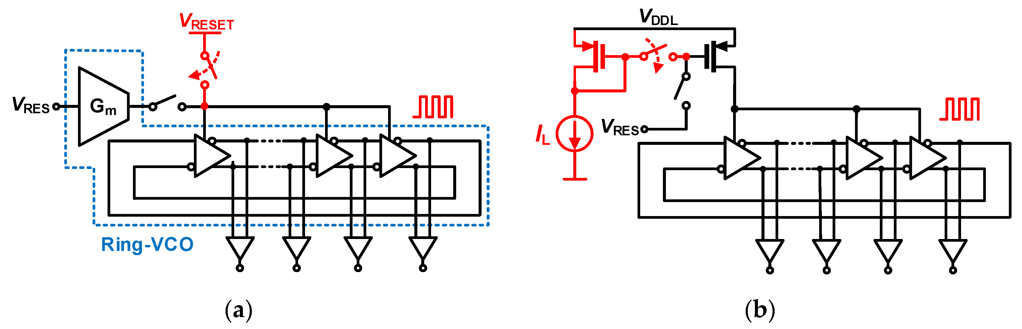
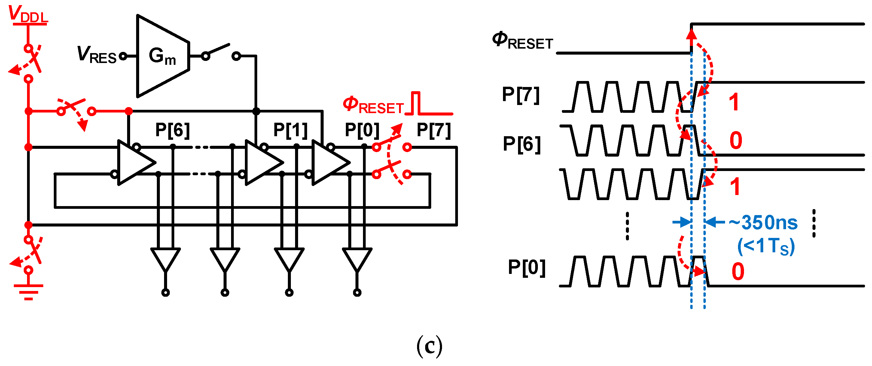
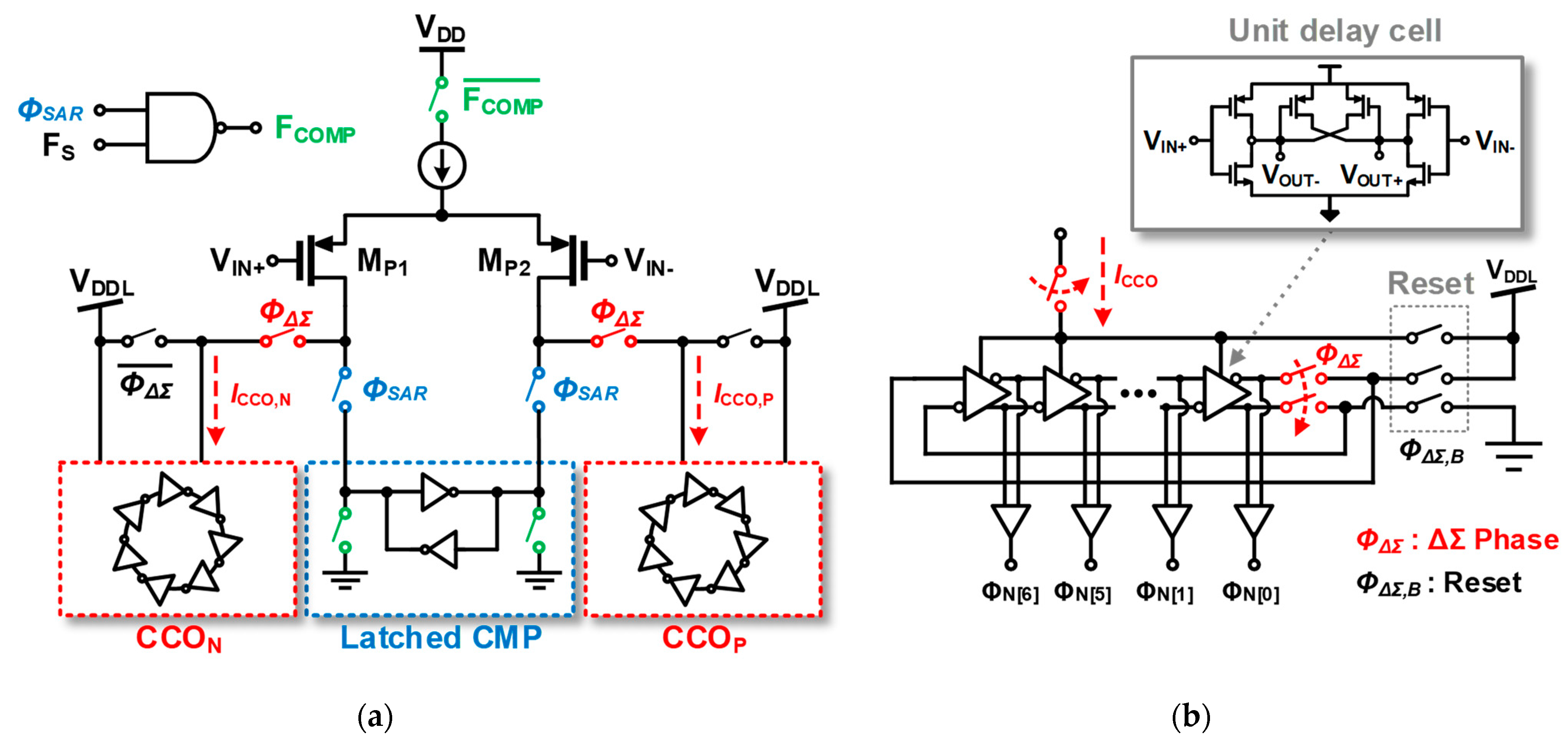
2.2. Ring-VCO-Based Time-Domain I-ΔΣM with Fast Phase-Reset

Since the VCO outputs a frequency proportional to the input voltage, it serves as a functional block of voltage to phase integrator in the phase domain. Using a ring-VCO as this VCO loop filter, the phase domain loop filter also has the characteristics of a multi-bit quantizer thanks to the ring-VCO’s multistage properties. When configured as a 7-stage ring-VCO, different 7-phases are generated by the phase difference (2π/7) from the reference phases. Furthermore, the ring-VCO modulates the mismatch of the unit capacitors in the feedback path to twice the center frequency of the VCO, since the basis of the 7-phases is changed every sampling phase by the frequency of the ring-VCO, which is known as the intrinsic clock level averaging (ICLA) [18]. Thanks to this inherent feature of the ring-VCO, no explicit dynamic element matching (DEM) or data weighted averaging (DWA) is required.
Figure 2a depicts a block diagram of an ΔΣ loop using a ring-VCO as a loop filter, a phase-frequency detector (PFD) used as a phase detector (PD), and D-flip flop (DFF) arrays as a sampler. The inherent ICLA of the ring-VCO is indicated as a dashed rectangle in Figure 2a. The ring-VCO makes the 7-phases relative to the reference phases, and the PFD arrays calculate the relative phase differences between them. The DFFs sample these phase differences. The sampled data are passed through the logic arrays to the output and feedback loop. When they are transferred to the feedback loop, they have the retiming latches to compensate for excess loop delay (ELD). The feedback path consists of the tri-level DACs with 4-bit output (not indicated in Figure 2a), all of which blocks make up the continuous time 1st-order ΔΣM. For the derivation of the mathematical descriptions of the given I-ΔΣM, each functional block can be redrawn with its own gain, as shown in Figure 2b. According to this, the loop filter of the ΔΣM can be given as:
L ( s ) = N K VCO K PFD T S 1 s
where KVCO, KPFD, N, and TS are the gains of the VCO and PFD, the number of consisting stages of the VCO, and sampling time, respectively. In our design, the KVCO, N, and FS (1/TS) are set as 163 MHz/V (KVCO = KCCO·Gm, where KCCO = 10.78 THz/A and Gm = 14 µS), 7, and 2.5 MHz, respectively. The KPFD is set as 1/2π since we have selected the PFDs as a quantizer. The loop gain is composed of the result of L(s) and the feedback factor, β = 1/512. The noise transfer function (NTF(z)) of the given 1st-order ΔΣM can be derived as:
N T F ( z ) = 1 z 1 1 ( 1 N K VCO β T S ) z 1
The out-of-band-gain (OBG) according to these values is designed to be a value of 1.5 to satisfy the stabilities due to the PVT variation of the VCO and the additional delay of the retiming latches.
To make the VCO-based ΔΣM work in the incremental mode, it is necessary to periodically reset the memory blocks, such as the VCO and PFDs, since the I-ΔΣM strictly requires no memory from its former inputs. Conventionally, there are two ways to reset the loop filter of VCOs: (1) break the loop and enforce a common mode (CM) voltage of the Gm cell (VRESET) [19], (2) apply a weak bias to the VCO (IL) [20], as shown in Figure 3a,b, respectively. In [19], when breaking the loop and enforcing the CM voltage (VRESET) of the Gm cell, an unintended offset may occur due to the difference between the enforcing voltage and the output CM voltage of the Gm cell by the PVT variation. It is also necessary to generate the CM voltage. The phase reset by applying a weak bias current to the VCO [20] consumes static current because it operates as a free-running VCO. This method can cause unintended phase noise at the beginning of the conversion since the initial phase is randomized. Thus, we enforce “1” and “0” logic states into the input of the differential ring-VCO in the reset phase, employing the low-side digital supply voltage (VDDL) instead of the additional reference voltage as shown in Figure 3c, making P [7:0] always be [10101010] within the round-trip time of the ring-VCO. This phase-alignment happens sufficiently fast, and at the same time the VCO does not consume any static power during the reset period of the fine converter. This is particularly useful for such a two-step incremental ADC as the coarse conversion usually occupies long duty. Figure 3c also depicts the conceptual transient waveforms. The fast phase-alignment has been done within only ~350 ns in post-simulation, which is less than 1TS. Since the alignment speed is proportional to the propagation delay of the 7-stage unit delay cell in VDDL, alignment is achieved at a faster rate by applying higher voltage than the swing of the CCO. One minor concern is the initialization time of the Gm cell when the VCO has to be out of the reset state. According to the SPECTRE simulation, the Gm recovers within ~150 ns, causing no performance degradation.

2.3. Noise Analysis

Since the inherent noise of the ADCs is the quantization noise, this has to be set sufficiently low when compared to other noise sources from sampling and active circuits. Accurately summing the coarse and fine outputs gives the quantization noise (υn,q) of the fine ADC as the value of the overall ADC. Due to the two-step architecture, υn,q is dependent on the LSB of the fine converter. The oversampling ratio of the I-ΔΣM is 16, so the value of the LSB is ~1/(519 ×∙16). Consequently, υn,q in this design has been set as 34.76 μVrms by allocating 8-bit for coarse and 4-bit (effectively, 6-bit) for fine conversions. This value is reasonable when aiming for 12-bit resolution, considering the full swing of the signals of 2 VP-P. Then, the sampling noise initially generated for the coarse conversion must also be considered. With a unit capacitance of 8-fF, a total of 519 capacitors in the CDAC sum up ~4.2-pF with parasitic capacitance, resulting in ~44.41 μVRMS of the sampling noise. Next, the noise from the active circuit in the incremental mode should be considered. In this case, the major noise source is the VCO that consists of the transconductance (Gm) cell and the current-controlled-oscillator (CCO). The thermal noise of the VCO is given as:
v n , t h e r m a l = ( 8 k T γ G m + i n , C C O 2 G m 2 ) f S 2 O S R Φ Δ Σ Φ T O T A L
where k, T, γ, ΦΔΣ, and ΦTOTAL are Boltzmann constant, absolute temperature, thermal noise coefficient of FET, ΔΣ, and entire conversion time, respectively. The current noise spectral density of the input-referred-noise of the 7-stage CCO according to SPECTRE simulation is 342 fA/√Hz [25] and Gm with the bias current of 1 μA is 14 μS. This results in the voltage noise spectrum density of 48.65 nV/√Hz by the 7-stage VCO. Since the sampling frequency is 2.5 MHz and fine mode operates 16 cycles out of a total of 25 cycles, the active cut-off frequency of thermal noises in incremental operation is assumed to be 80-kHz processed by decimation filters. This yields thermal noise value of 15.40 μVrms with ΦTOTAL = 25 and ΦΔΣ = 16 according to (4). In addition, the low frequency noise (1/f) generated by the active device has a cut-off frequency of ~900 Hz through SPECTRE noise simulation. The integrated noise value of 1/f noise from 1 Hz to 50 kHz is ~4 μVrms. The overall noise induced by the active circuit is 15.91 μVrms.
The digital output of the presented ADC is the sum of the SAR and I-ΔΣM outputs. A gain mismatch between these two digital outputs can cause spectral leakages [26,27]. To mitigate this issue, the design incorporates a DAC configured with identical unit capacitors, while employing a shared Gm for integration. Furthermore, the input range of the fine ADC has been set 3.5 times the LSB of the coarse quantizer for redundancy. In addition, to simplify the processing of the two values, the CDACs of coarse-fine are constructed via a ratio in a unit capacitance design, as described in Section 2.1. The incremental ADC is configured in continuous-time, which introduces STF leakage by gain mismatch due to the initial settling time and the finite OSR. The first sample by initial settling time has an error value. This error is mitigated by the OSR, which is calculated as a ~2.3% gain error in G2 for the specified gain by the ratio of CDAC in (1). The gain mismatch results in a ~0.1 dB SNDR degradation when targeting 12-bit resolution, so it is not the issue.

3. Circuit Implementations

The proposed ADC comprises circuit blocks including a bootstrapped S/H circuit, an 8-bit synchronous SAR ADC, and an I-ΔΣM consisting of loop filter with Gm-CCO (VCO), phase quantizer with PFD, and DFF. The SAR ADC and I-ΔΣM are organized in a two-step ADC with each sharing input Gm and CDAC. The CDAC consists of 512C of SAR for feedback to configure 8-bit conversion and 8-bit resolution coarse residual voltage and 7C of 7-stage ring-VCO for tri-level switching. The unit capacitance of SAR CDAC has 2C consisting of two unit capacitors (C) and is configured as an 8-bit CDAC to provide an 8-bit top-plate residual voltage. Each unit capacitor (C) is split into two 4-fF finger-type custom MOM capacitors [28], each with a digital code for tri-level switching. The MOM capacitor is configured using a metal 5 layer to minimize the parasitic capacitance and maximize the effective coupling capacitance between the top plate and bottom plate in the 1P6M 180 nm process, and the MOM capacitance was verified by CALIBRE parasitic extraction. The overall parasitic capacitance and effective coupling capacitance of the top plate are 0.291-pF and 4.15-pF, respectively. A simplified schematic block diagram is shown in Figure 4. In the sample-phase, the input is sampled to the CDAC. After that, a comparator consisting of Gm and the current latch synchronously converts the top-plate voltage of the CDAC to the digital bit, depending on the clock, to operate the SAR ADC. Once the SAR has processed 8-bit conversion, the Gm stage disconnects from the latch and connects to the 7-stage ring-CCO to form the closed loop filter. The I-ΔΣM, in incremental mode with the loop filter composed of Gm-CCO, performs fine conversion on the residual voltage after SAR conversion. The phase outputs of each 7-stage ring-CCO are converted to 14-bit thermometer codes for up/down through the PFD arrays for phase quantizer. Each code is then sampled by the DFF arrays and passed through the encoder arrays for tri-level switching and propagation delay error suppression. The processed digital codes are fed back through the retiming latch equal to the delay of z−1/8 to effectively handle excess loop delay.
The circuits that process the phase outputs of the ring-CCO behave like digital circuits. In a digital circuit, power consumption is proportional to the square of the supply voltage, and the operating speed decreases rapidly below a threshold voltage. While energy efficiency can be increased by reducing the supply voltage, the operation can be limited by the reduced operating speed. For high energy efficiency, the low supply voltage of VDDL is used for processing the phase outputs for feedback latch, and the additional supply voltage of VDD is used for the dynamic range of the proposed incremental zoom ADC. The entire system consists of the dual supply of VDD, 1 V and VDDL, 0.55 V. The frequency of main clock source (FS) is 2.5 MHz. For one analog input, eight cycles are allocated for the SAR conversion, one cycle for top-plate sampling, and 16 cycles for delta-sigma operation, for a total of 25 cycles. The presented ADC has a sampling rate of 100-kS/s and a bandwidth of 50-kHz.

3.1. Voltage-Controlled Oscillator

The VCO is implemented by a Gm-stage-driven current-controlled oscillator (CCO). The schematic of the VCO is shown in Figure 5a. During the ΦSAR, the VCO is configured into a latched comparator consisting of Gm and the current latch, disabling the CCOs. After that, it is reconfigured into a VCO and used as the loop filter of I-ΔΣM in the ΦΔΣ. The schematics of its internal dual ring CCO are shown in Figure 5b. Instead of using the current reusing topology for the Gm stage that provides higher gm/Id efficiency and accompanies the compensation circuit for low-supply usages, a single PMOS input has been used to reduce circuit design complexity. The CCO blocks consist of 7-stage unit delay cells and several switches for the fast phase-alignment. The unit cell has been implemented as pseudo-differential with PMOS cross-coupled pair for lower phase noise and higher gain of current to frequency (KCCO) with unit delay cell [19]. The output swing of each node is 0.45 V, which is sufficient for the VDDL of 0.55 V. Instead of a level shifter for driving the PFD arrays, a differential buffer is used to output the digital signal for each phase. As mentioned in the previous section, with just four switches on the dual ring-CCOs, the fast phase-alignment of the VCO-based I-ΔΣM is effectively completed.

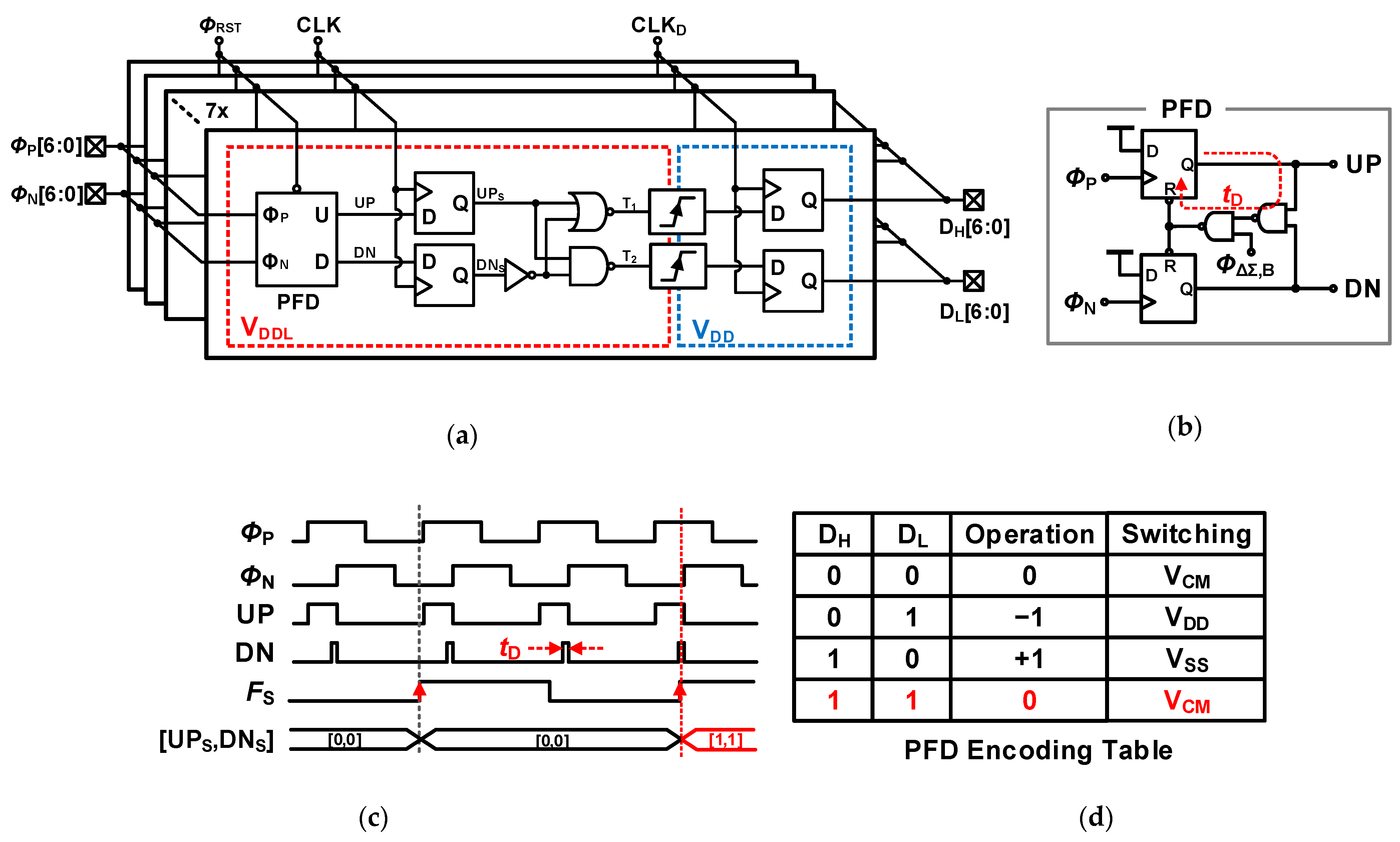
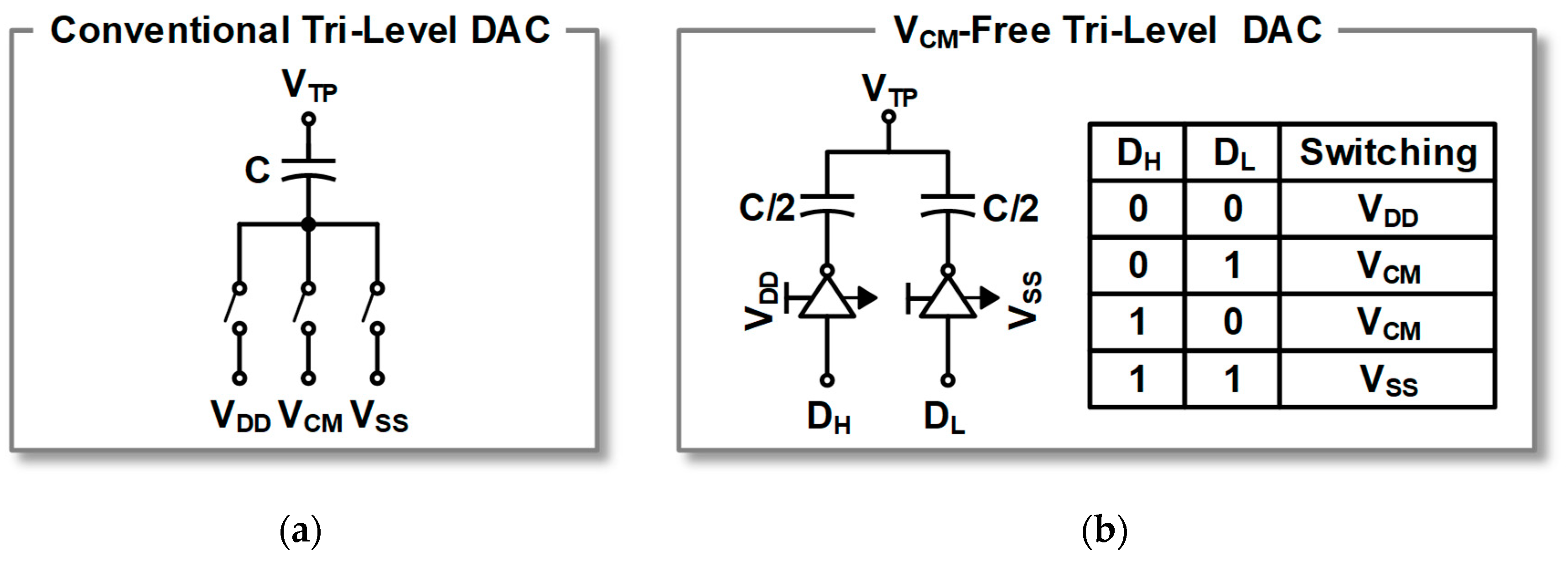
3.2. Phase Frequency Dectector-Based Phase Quantizer and VCM-Free Tri-Level Unit Capacitor

For the initial developments of the quantizer for the VCO-based ADCs, the XOR gates and the phase extended quantizer (PEQ) have been widely adopted [29]. However, their limited resolvable phase range and implementation complexity called for the phase-frequency detector (PFD)-based phase quantizer. The PFD-based quantizer can ensure full range (−2π to 2π) detection of the VCO phase information. In addition to that, a double PFD (DPFD) quantizer was recently introduced which is able to cover 2× wider range of phase (−4π to 4π) by detecting both of rising and falling edges, providing the same amount of less quantization noise [30]. However, the duty ratio of the DPFD may cause a non-linearity effect in the quantizer of the Δ-Σ loop, which causes additional noise since it heavily counts on the exact timings of the rising and falling edges of D-flip flops (D-FFs), stumbling its wide usage for the applications where the aggressive voltage scaling for the digital circuits is highly required. For the proposed ADC, the PFD has been adopted because near-threshold supply of 0.55 V in the given 180 nm process was used to aggressively squeeze the power consumption.
The digital circuit facilitates the feedforward and feedback paths of the proposed Δ-Σ. As shown in Figure 6a, this block consists of PFD arrays for phase quantization, D-FF arrays for sampling of phase information, and logics for tri-level switching in the forward path, level shifters to drive feedback path, and retiming. The schematic of the PFD is also shown in Figure 6b. Since the PFD has memory, it stores the previous value. For this reason, ΦΔΣ-B is added to reset the PFD. In the proposed design, a low power supply of 0.55 V(VDDL) for the phase quantization and a higher supply of 1.0 V (VDD) for retiming of the acquired phase information are used to minimize the dynamic power consumption. As a result, the propagation delay (tD) of the DN signal can generate an error state of [1, 1] when synchronized with the sampling clock (FS) as shown in Figure 6c. Rather than ignoring such intermittently generated errors and leaving an open state, the [1, 1] state has been assigned to activate the common mode voltage (VCM) by using a tri-level DAC in this work.
The tri-level DAC can double the resolution, however it requires an additional feedback path driven by the well-defined common mode voltage (VCM) of the other two feedback references, such as VDD and ground (VSS), as shown in Figure 7a. In this implementation, the VCM-free tri-level unit DAC, where the two same parallel connected capacitors are driven by DH and DL, can generate the well-defined VCM without any explicit reference generation circuit (Figure 7b), in other words, without any static power and area consumptions. The error of the VCM can only be caused by the mismatch of the two capacitors of 8-fF (<0.5%) [31]. In [32], a pair of JK flip flop has been added to attenuate the capacitor mismatch in the unit capacitor DAC, but the SNDR degradation has been found to be very minute according to our extensive simulations.

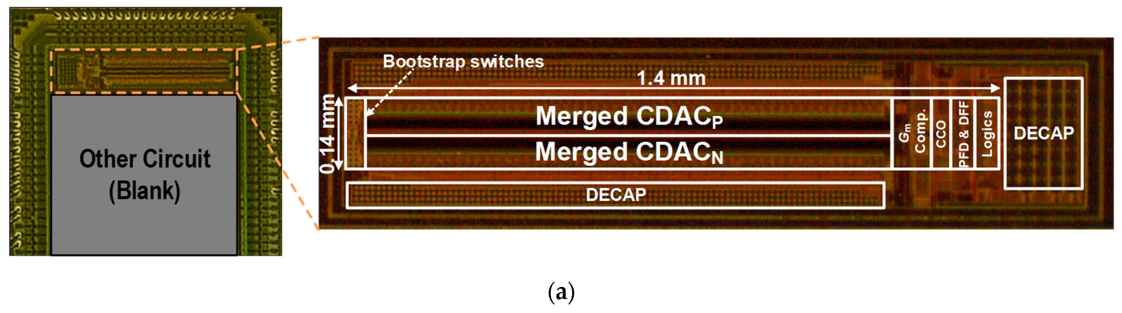
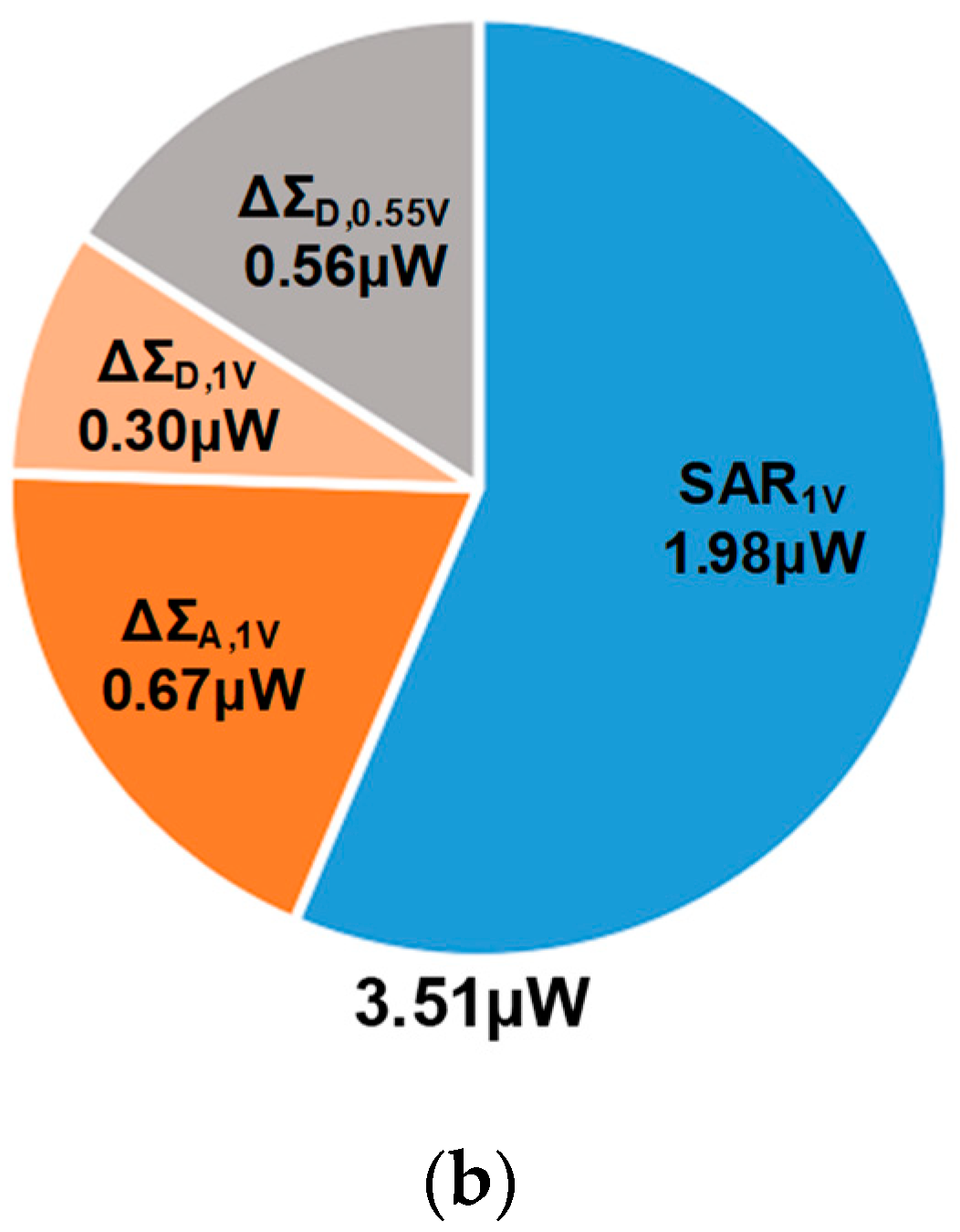
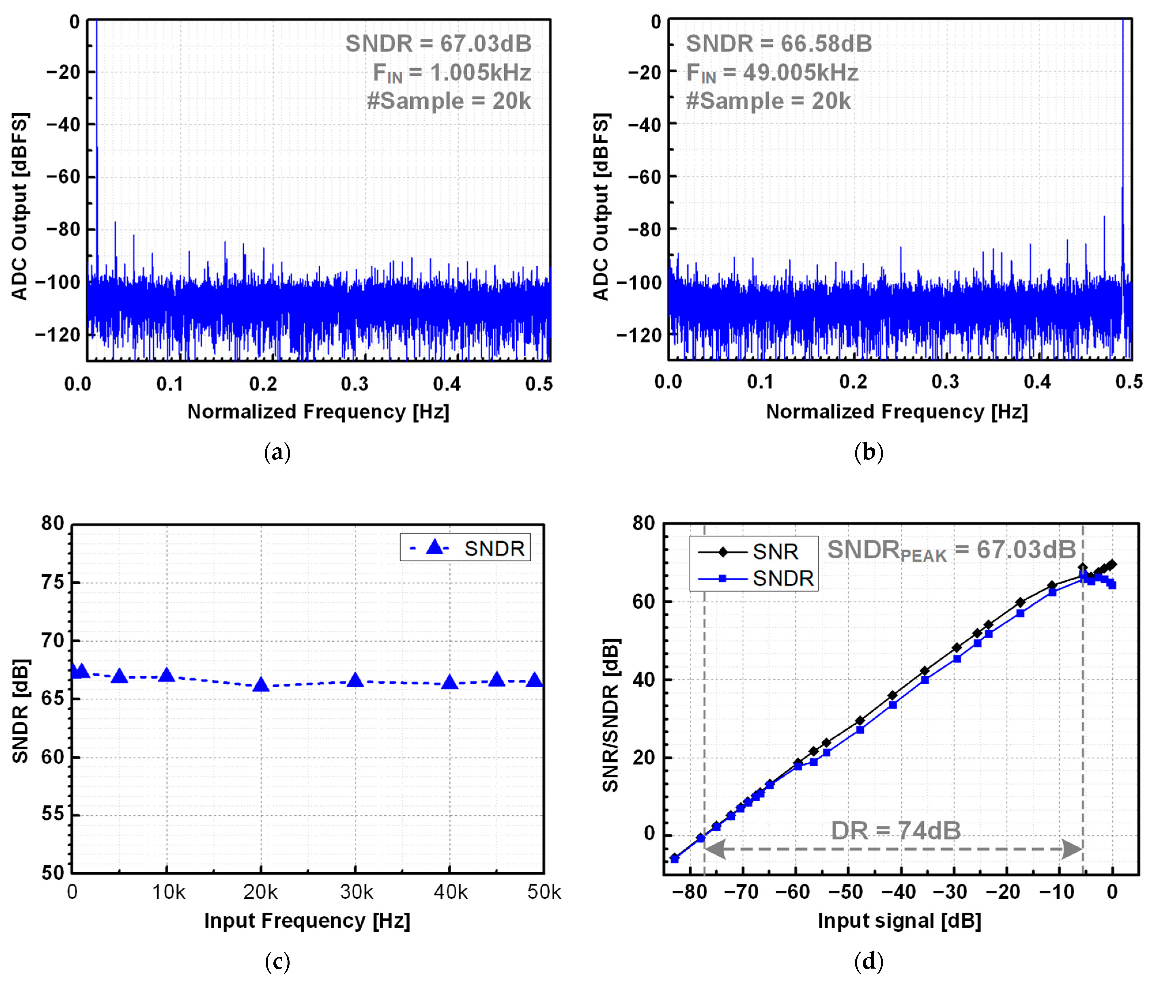
4. Measurement Results

The prototype zoom ADC has been fabricated using the standard 180 nm 1P6M CMOS process. The die microphotograph of the fabricated ADC is depicted in Figure 8a. It occupies 0.196 mm2 of active area. The area of the active circuit without the merged CDAC is relatively small due to the simplicity of implementation. The digital bit outputs are processed by the off-chip FPGA that combines the output of the SAR ADC and the output of the I-ΔΣ modulator as explained in Figure 1.
The measurement setup is depicted in Figure 9. The measurement equipment is a function generator (DS360, SRS) to apply the differential input signals, a power supply (2231A, KEITHLEY), a source meter (2450, KEITHLEY) to estimate power consumption by measuring current, and LabVIEW DAQ (NI) to process the data from the FPGA on a PC. The power supply powers the LDO board and the FPGA board, as shown in Figure 9(right). The LDO board provides 1 V (VDD), 0.55 V (VDDL), and 1.8 V for transmitting the ADC digital output to the FPGA and driving electrostatic discharge (ESD) protection diode, respectively. The power measurement is measured by disconnecting VDDL and measuring the average current with the source meter to estimate the power consumed by VDDL, as shown in Figure 9(left). The same method is used for the power dissipated by VDD.
The presented ADC uses the main frequency of 2.5 MHz and has the highest sampling rate of 100 kS/s with a total of 25 phases. The analog supply is 1.0 V (VDD), while the digital supply for operation with logic of the I-ΔΣ is 0.55 V (VDDL) to enhance the power-efficiency. No other external supply voltage has been used except these two. The overall power consumption was measured as 3.51 μW. The detailed power consumption breakdown is shown in Figure 8b. The SAR ADC consumes 1.98 μW of power, while the I-ΔΣ consumes 0.56 μW from VDDL, the level shifter, retiming latch, and switching power from VDD consume 0.30 μW, and the Gm operation consumes 0.67 μW of power from VDD. These values were estimated by measuring the power consumed by each supply and dividing by the portion of power it accounts for in the post-simulation result.
The digital outputs of the presented ADC for analog inputs were passed through the FPGA to LabVIEW and stored in the PC, and the dynamic performance of the ADC was processed using MATLAB. The FFT plots for two extreme input frequencies of 1.005 kHz and 49.005 kHz are shown in Figure 10a,b. For this measurement, 20,000 samples have been collected with a 1.0 Vp-p input sinusoidal amplitude. The SNDRs for the two cases were calculated as 67.03-dB and 66.58-dB, respectively. Based on those, the maximum effective number of bits (ENOB = (SNDR−1.76)/6.02) has been calculated as 10.84. In addition to those, other input frequencies from 100 Hz to 49 kHz with 1.0 Vp-p inputs were also measured and are summarized in Figure 10c. All SNDR are distributed over 66.5-dB. It indicates that the performance of the ADC is nearly independent of the input frequency. Since the fine ADC converts the residual voltage of the coarse ADC as a DC voltage when operating it, if it can be sampled appropriately, the SNDR of the output doesn’t dependent on the variation of the input frequency. The SNDR measurement with respect to the input voltage amplitude has also been performed as shown in Figure 10d. A dynamic range of 74-dB and 67-dB in terms of SNR and SNDR, respectively, has been obtained at −6-dB input (1.0 Vp-p). A bit early saturation of the SNDR may come from the non-linear body effect of the implemented bootstrapped S/H.
Table 1 summarizes the performance of the fabricated ADC and compares it with other state-of-the-art ADCs. The presented ADC used in this work is a two-step ADC with the I-ΔΣ based on multi-bit quantizer with VCO and SAR ADC. Compared to other ADCs with similar ENOB and SNDR, this ADC has the best figure of merit (FoM). Also, this digital-friendly ADC can exhibit higher performance through enhanced process in addition to improvements in the modified sampling switch.

5. Conclusions

In this work, we present an energy-efficient 12-bit, 100 kS/s zoom ADC consisting of the coarse SAR and the fine VCO-based incremental ΔΣM for battery-operated multichannel biomedical devices. To accommodate multichannel biomedical signals without channel-to-channel phase leakage, the fast phase-alignment scheme in the VCO is proposed and designed with the zoom ADC. In addition, the VCM-free unit DAC is adopted for high energy efficiency and simple implementation. The proposed ADC has been fabricated in the standard 180 nm CMOS process, exhibiting 67-dB peak SNDR, 19.12 fJ/c-s of Walden, and 168.5-dB of Schrier FoM, respectively. Those performance metrics are the best FoM when compared with other state-of-the-art two-step ADCs.

Author Contributions

Conceptualization, J.K. and S.-Y.P.; methodology, J.K.; software, J.K. and S.-Y.P.; validation, J.K. and S.-Y.P.; formal analysis, J.K.; investigation, J.K.; resources, S.-Y.P.; data curation, J.K.; writing—original draft preparation, J.K.; writing—review and editing, S.-Y.P.; visualization, J.K.; supervision, S.-Y.P.; project administration, S.-Y.P.; funding acquisition, S.-Y.P. All authors have read and agreed to the published version of the manuscript.

Funding

This work was supported by National Research Foundation of Korea (NRF) grant funded by the Korea government (MSIT) (2020R1A2C2101875). This research was also supported by BK21PLUS, Creative Human Resource Education and Research Programs for ICT Convergence in the 4th Industrial Revolution.

Data Availability Statement

Data are contained within this article. The raw data supporting the conclusions of this article will be made available by the author on reasonable request.

Acknowledgments

The EDA Tools was supported by IC Design Education Center (IDEC).

Conflicts of Interest

The authors declare no conflicts of interest.

References

  1. Won, S.M.; Cai, L.; Gutruf, P.; Rogers, J.A. Wireless and battery-free technologies for neuroengineering. Nat. Biomed. Eng. 2021, 7, 405–423. [Google Scholar] [CrossRef] [PubMed]
  2. Yakovlev, A.; Kim, S.; Poon, A. Implantable biomedical devices: Wireless powering and communication. IEEE Commun. Mag. 2012, 50, 152–159. [Google Scholar] [CrossRef]
  3. Mendrela, A.E.; Park, S.-Y.; Voroslakos, M.; Flynn, M.P.; Yoon, E. A Battery-Powered Opto-Electrophysiology Neural Interface with Artifact-Preventing Optical Pulse Shaping. In Proceedings of the 2018 IEEE Symposium on VLSI Circuits, Honolulu, HI, USA, 18–22 June 2018; pp. 125–126. [Google Scholar]
  4. Wang, H.; Wang, X.; Barfidokht, A.; Park, J.; Wang, J.; Mercier, P.P. A Battery-Powered Wireless Ion Sensing System Consuming 5.5 nW of Average Power. IEEE J. Solid-State Circuits 2018, 53, 2043–2053. [Google Scholar] [CrossRef]
  5. Azin, M.; Guggenmos, D.J.; Barbay, S.; Nudo, R.J.; Mohseni, P. A Battery-Powered Activity-Dependent Intracortical Microstimulation IC for Brain-Machine-Brain Interface. IEEE J. Solid-State Circuits 2011, 46, 731–745. [Google Scholar] [CrossRef]
  6. Seymour, J.P.; Wu, F.; Wise, K.D.; Yoon, E. State-of-the-art MEMS and microsystem tools for brain research. Microsyst. Nanoeng. 2017, 3, 16066. [Google Scholar] [CrossRef] [PubMed]
  7. Jochum, T.; Denison, T.; Wolf, P. Integrated Circuit Amplifiers for Multi-Electrode Intracortical Recording. J. Neural Eng. 2009, 6, 012001. [Google Scholar] [CrossRef]
  8. Oh, S.; Song, H.; Slager, N.; Ruiz, J.R.L.; Park, S.-Y.; Yoon, E. Power-Efficient LFP-Adaptive Dynamic Zoom-and-Track Incremental ΔΣ Front-End for Dual-Band Subcortical Recordings. IEEE Trans. Biomed. Circuits Syst. 2023, 17, 741–753. [Google Scholar] [CrossRef]
  9. Oh, S.; Kim, K.; Roberto, J.; Ruiz, L.; Slager, N.; Ko, E. A compact, ultrahigh-density headstage with high-fidelity hybrid integration for large-scale deep-brain opto-electrophysiology. bioRxiv 2023. [Google Scholar] [CrossRef]
  10. Park, S.-Y.; Cho, J.; Lee, K.; Yoon, E. Dynamic Power Reduction in Scalable Neural Recording Interface Using Spatiotemporal Correlation and Temporal Sparsity of Neural Signals. IEEE J. Solid-State Circuits 2018, 53, 1102–1114. [Google Scholar] [CrossRef]
  11. Park, S.-Y.; Cho, J.; Na, K.; Yoon, E. Modular 128-Channel Δ − ΔΣ Analog Front-End Architecture Using Spectrum Equalization Scheme for 1024-Channel 3-D Neural Recording Microsystems. IEEE J. Solid-State Circuits 2017, 53, 501–514. [Google Scholar] [CrossRef]
  12. Huang, X.; Londoño-Ramírez, H.; Ballini, M.; Van Hoof, C.; Genoe, J.; Haesler, S.; Gielen, G.; Van Helleputte, N.; Lopez, C.M. A 256-Channel Actively-Multiplexed μECoG Implant with Column-Parallel Incremental ΔΣ ADCs Employing Bulk-DACs in 22-nm FDSOI Technology. In Proceedings of the 2022 IEEE International Solid-State Circuits Conference (ISSCC), San Francisco, CA, USA, 20–26 February 2023; pp. 22–24. [Google Scholar] [CrossRef]
  13. Sadollahi, M.; Hamashita, K.; Sobue, K.; Temes, G.C. An 11-Bit 250-nW 10-kS/s SAR ADC With Doubled Input Range for Biomedical Applications. IEEE Trans. Circuits Syst. I Regul. Pap. 2017, 65, 61–73. [Google Scholar]
  14. Hariprasath, V.; Guerber, J.; Lee, S.-H.; Moon, U.-K. Merged capacitor switching based SAR ADC with highest switching energy-efficiency. Electron. Lett. 2010, 46, 620–621. [Google Scholar] [CrossRef]
  15. Hsieh, S.-E.; Hsieh, C.-C. A 0.44-fJ/Conversion-Step 11-Bit 600-kS/s SAR ADC With Semi-Resting DAC. IEEE J. Solid-State Circuits 2018, 53, 2595–2603. [Google Scholar] [CrossRef]
  16. Chae, Y.; Souri, K.; Makinwa, K.A.A. A 6.3 µW 20 bit Incremental Zoom-ADC with 6 ppm INL and 1 µV Offset. IEEE J. Solid-State Circuits 2013, 48, 3019–3027. [Google Scholar] [CrossRef]
  17. Straayer, M.Z.; Perrott, M.H.; Concepts, A.B. A 12-Bit, 10-MHz Bandwidth, Continuous-Time Sigma-Delta ADC with a 5-Bit, 950-MS/s VCO-Based Quantizer. IEEE J. Solid-State Circuits 2009, 43, 805–814. [Google Scholar] [CrossRef]
  18. Lee, K.; Yoon, Y.; Sun, N. A Scaling-Friendly Low-Power Small-Area ΔΣ ADC With VCO-Based Integrator and Intrinsic Mismatch Shaping Capability. IEEE J. Emerg. Sel. Top. Circuits Syst. 2015, 5, 561–573. [Google Scholar] [CrossRef]
  19. Tang, X.; Li, S.; Yang, X.; Shen, L.; Zhao, W.; Williams, R.P.; Liu, J.; Tan, Z.; Hall, N.A.; Pan, D.Z.; et al. An Energy-Efficient Time-Domain Incremental Capacitance-to-Digital Converter. IEEE J. Solid-State Circuits 2020, 55, 3064–3075. [Google Scholar] [CrossRef]
  20. Sanyal, A.; Sun, N. An Energy-Efficient Hybrid SAR-VCO ΔΣ Capacitance-to-Digital Converter in 40-nm CMOS. IEEE J. Solid-State Circuits 2017, 52, 1966–1976. [Google Scholar] [CrossRef]
  21. Liu, H.; Guo, T.; Yan, P.; Qi, L.; Chen, M.; Wang, G.; Liu, Y. A Hybrid 1st/2nd-order VCO-based CTDSM with Rail-to-Rail Artifact Tolerance for Bidirectional Neural Interface. IEEE Trans. Circuits Syst. II Express Briefs 2022, 69, 2682–2686. [Google Scholar] [CrossRef]
  22. Hsieh, S.-E.; Hsieh, C.-C. A 0.4-V 13-bit 270-kS/s SAR-ISDM ADC With Opamp-Less Time-Domain Integrator. IEEE J. Solid-State Circuits 2019, 54, 1648–1656. [Google Scholar] [CrossRef]
  23. Markus, J.; Silva, J.; Temes, G. Theory and Applications of Incremental ΔΣ Converters. IEEE Trans. Circuits Syst. I Regul. Pap. 2004, 51, 678–690. [Google Scholar] [CrossRef]
  24. Hsieh, C.; Liu, S. A 0.3V 10bit 7.3fJ/conversion-step SAR ADC in 0.18 μm CMOS. In Proceedings of the 2014 IEEE Asian Solid-State Circuits Conference (A-SSCC), KaoHsiung, Taiwan, 10–12 November 2014; pp. 31–34. [Google Scholar] [CrossRef]
  25. Ham, D.; Hajimiri, A. Virtual damping and einstein relation in oscillators. IEEE J. Solid-State Circuits 2003, 38, 407–418. [Google Scholar] [CrossRef]
  26. Eland, E.; Karmakar, S.; Gonen, B.; van Veldhoven, R.; Makinwa, K.A.A. A 440-μW, 109.8-dB DR, 106.5-dB SNDR Discrete-Time Zoom ADC With a 20-kHz BW. IEEE J. Solid-State Circuits 2021, 56, 1207–1215. [Google Scholar] [CrossRef]
  27. Karmakar, S.; Gonen, B.; Sebastiano, F.; van Veldhoven, R.; Makinwa, K.A.A. A 280 µW Dynamic Zoom ADC With 120 dB DR and 118 dB SNDR in 1 kHz BW. IEEE J. Solid-State Circuits 2018, 53, 3497–3507. [Google Scholar] [CrossRef]
  28. Harpe, P.J.A.; Zhou, C.; Bi, Y.; van der Meijs, N.P.; Wang, X.; Philips, K.; Dolmans, G.; de Groot, H. A 26 μW 8 bit 10 MS/s Asynchronous SAR ADC for Low Energy Radios. IEEE J. Solid-State Circuits 2011, 46, 1585–1595. [Google Scholar] [CrossRef]
  29. Li, S.; Mukherjee, A.; Sun, N. A 174.3-dB FoM VCO-Based CT ΔΣ Modulator with a Fully-Digital Phase Extended Quantizer and Tri-Level Resistor DAC in 130-nm CMOS. IEEE J. Solid-State Circuits 2017, 52, 1940–1952. [Google Scholar] [CrossRef]
  30. Zhong, Y.; Tang, X.; Liu, J.; Zhao, W.; Li, S.; Sun, N. An 81.5dB-DR 1.25MHz-BW VCO-Based CT ΔΣ ADC with Double-PFD Quantizer. In Proceedings of the 2021 IEEE Custom Integrated Circuits Conference (CICC), Austin, TX, USA, 25–30 April 2021; pp. 5–6. [Google Scholar] [CrossRef]
  31. Omran, H.; Alahmadi, H.; Salama, K.N. Matching Properties of Femtofarad MOM Capacitors. IEEE Trans. Circuits Syst. I Regul. Pap. 2016, 63, 763–772. [Google Scholar] [CrossRef]
  32. Zhao, W.; Li, S.; Xu, B.; Yang, X.; Tang, X.; Shen, L.; Lu, N.; Pan, D.Z.; Sun, N. A 0.025-mm2 0.8V 78.5dB VCO-Based Sensor Readout Circuit in a Hybrid PLL-ΔΣ M Structure. IEEE J. Solid-State Circuits 2019, 55, 666–679. [Google Scholar] [CrossRef]
  33. Hu, J.; Li, D.; Liu, M.; Zhu, Z. A 10-kS/s 625-Hz-Bandwidth 65-dB SNDR Second-Order Noise-Shaping SAR ADC for Biomedical Sensor Applications. IEEE Sens. J. 2019, 20, 13881–13891. [Google Scholar] [CrossRef]
  34. Moon, C.W.; Yoon, K.S.; Lee, J. A 12~14-Bit SAR-SS Hybrid ADC with SS Bit Shifting Resolution Reconfigurable Method for Bio-Signal Processing. Electronics 2023, 12, 4916. [Google Scholar] [CrossRef]
  35. Zhang, Q.; Ning, N.; Zhang, Z.; Li, J.; Wu, K.; Yu, Q. A 12-Bit Two-Step Single-Slope ADC With a Constant Input-Common-Mode Level Resistor Ramp Generator. IEEE Trans. Very Large Scale Integr. Syst. 2022, 30, 644–655. [Google Scholar] [CrossRef]
  36. Hu, Y.; Huang, Q.; Tang, B.; Chen, C.; Hu, L.; Yu, E.; Li, B.; Wu, Z. A Low-Power SAR ADC with Capacitor-Splitting Energy-Efficient Switching Scheme for Wearable Biosensor Applications. Micromachines 2023, 14, 2244. [Google Scholar] [CrossRef] [PubMed]
Figure 1. (a) Overall architecture of the proposed incremental zoom ADC, (b) timing diagram of the proposed ADC.
Electronics 13 01754 g001
Figure 2. (a) Block diagram of 1st-order VCO-based ΔΣM, (b) mathematical description of (a) for coefficient extractions.
Electronics 13 01754 g002aElectronics 13 01754 g002b
Figure 3. Conventional ring-VCO reset mechanisms (a) [19], (b) [20] and, (c) proposed phase-alignment of ring-VCO (left) and conceptual operation (right).
Electronics 13 01754 g003aElectronics 13 01754 g003b
Figure 4. Top-level schematic block diagram of the proposed incremental zoom ADC.
Electronics 13 01754 g004
Figure 5. (a) Schematics of the current comparator (blue dashed) and the VCO consisting of Gm stage and CCOs (red dashed), and (b) 7-stage dual ring-CCO with unit delay cell (gray).
Electronics 13 01754 g005
Figure 6. (a) Overall logic implementations, (b) operation behavior of PFD, (c) positive input phase waveforms, (d) logic mapping.
Electronics 13 01754 g006
Figure 7. Conventional tri-level switching DAC (a), and VCM-free, tri-level switching DAC used in this work (b).
Electronics 13 01754 g007
Figure 8. (a) A die photograph of the presented incremental zoom ADC, (b) power breakdown.
Electronics 13 01754 g008aElectronics 13 01754 g008b
Figure 9. Measurement setup (left) and photograph of measurement setup (right).
Electronics 13 01754 g009
Figure 10. Measured ADC output spectrum at (a) 1.005 kHz, (b) 49.005 kHz, (c) input frequency to SNDR plot with 1VP-P sine wave input, (d) signal to SNR/SNDR plot.
Electronics 13 01754 g010
Table 1. ADC performance summary and comparison with state-of-the-art works.
[21][33][34][35][36]This Work
Process (nm)4018028130180180
ArchitectureSAR + VCONS-SARSAR-SSTS SSSARSAR + I-ΔΣM
Supply (V)1.8113.3/1.211.0(A)/0.55(D)
Power (μW)41000.0934624.453.51
SNDR (dB)75.76566.8 *60.7861.7767
BW (kHz)35000.625205010050
ENOB (bits)12.2810.510.819.89.9710.84
FoMW 1 (fJ/conv.)382505369622.219.12
FoMS 2 (dB)165 *163 *164 *150 *165 *168.5
* Calculated. 1 Walden Figure-of-Merits (FoMW) = Power/(FS  × 2ENOB). 2 Schreier FoMS = SNDR + 10log (BW/Power).
Disclaimer/Publisher’s Note: The statements, opinions and data contained in all publications are solely those of the individual author(s) and contributor(s) and not of MDPI and/or the editor(s). MDPI and/or the editor(s) disclaim responsibility for any injury to people or property resulting from any ideas, methods, instructions or products referred to in the content.

