
An Energy Consumption Model for SRAM-Based In-Memory-Computing Architectures


Abstract
1. Introduction
- (1)
- A fully analytical model is proposed to estimate the power and switching activity factor of IMC-based architectures. Using our model, designers can pre-estimate overall power consumption in seconds with an accuracy close to NeuroSim.
- (2)
- The switching activity factors for MNIST-like datasets as well as the CIFAR-10 dataset are computed. Designers can use these activity factors to improve their power estimations.
- (3)
- An optimization for lowering the switching activity while maintaining high resolution is proposed. It is shown that this optimization can be completed in orders of magnitude shorter time compared to other simulation methods.
2. Related Works
2.1. Software Simulation for Estimation of IMC Performance
2.2. Emulation in FPGA for Estimation of IMC
2.3. Analytical Model for Estimation of IMC
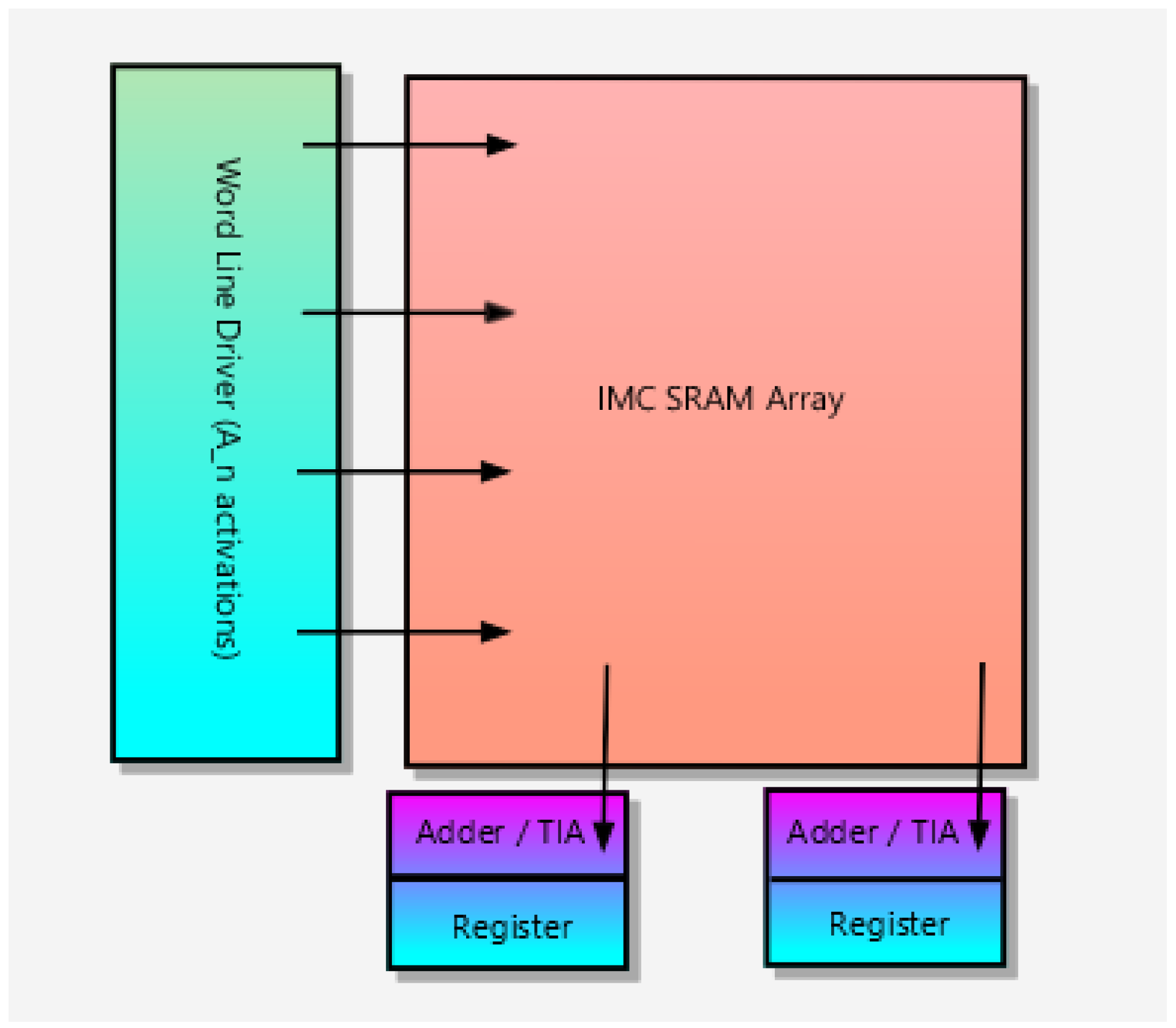
3. Background
3.1. Binary Multiplication Phase
3.2. Accumulation Phase
4. Mathematical Model
4.1. Switching Activity Factor
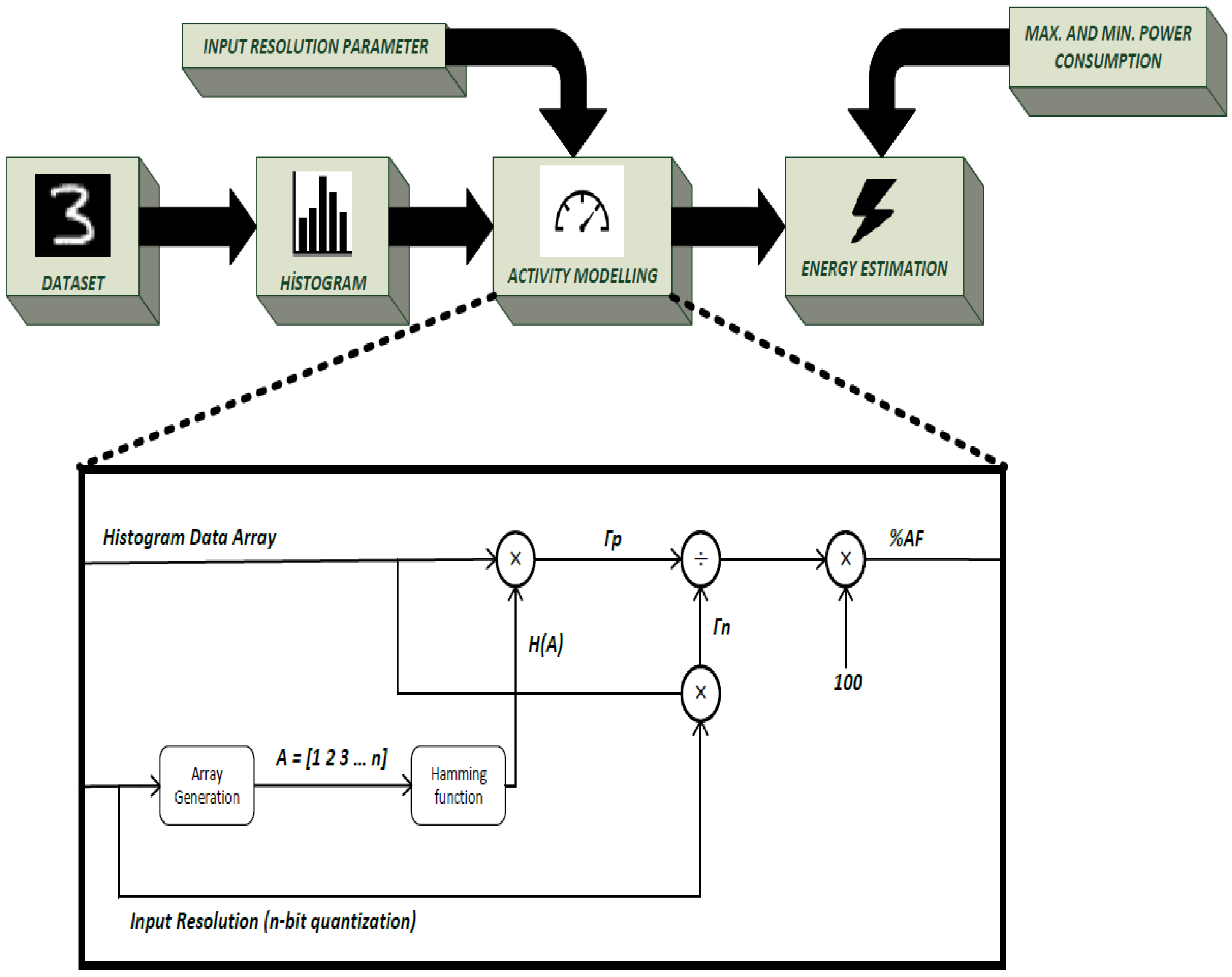
4.2. Quantization and Histogram of Activation Data
4.3. Energy Modeling
4.4. Framework of Our Energy Estimation Model
5. Results
5.1. Comparison of Proposed Analytical Model against NeuroSim
5.2. Switching Activity Factor List
5.3. Example of Fast Optimization Using the Analytical Model: Reducing Activity by Optimizing Input Quantization
6. Conclusions and Future Works
- Introducing a very quick power estimation tool that can be very helpful during architectural explorations;
- Tabulating switching activity factors for some appropriate datasets, such as MNIST-like datasets as well as the CIFAR-10 dataset;
- Providing an example use of our algorithm. Here, we proposed an optimization for lowering the switching activity while maintaining high resolution. We showed that this optimization can achieve energy reductions up to 53% while completing in orders of magnitude shorter simulation times compared to other simulation methods.
Author Contributions
Funding
Data Availability Statement
Conflicts of Interest
References
- Park, J.S.; Na, H.J. Front-End of Vehicle-Embedded Speech Recognition for Voice-Driven Multi-UAVs Control. Appl. Sci. 2020, 10, 6876. [Google Scholar] [CrossRef]
- Yin, S.; Ouyang, P.; Zheng, S.; Song, D.; Li, X.; Liu, L.; Wei, S. A 141 UW, 2.46 PJ/Neuron Binarized Convolutional Neural Network Based Self-Learning Speech Recognition Processor in 28NM CMOS. In Proceedings of the 2018 IEEE Symposium on VLSI Circuits, Honolulu, HI, USA, 18–22 June 2018; pp. 139–140. [Google Scholar] [CrossRef]
- Shan, W.; Yang, M.; Wang, T.; Lu, Y.; Cai, H.; Zhu, L.; Xu, J.; Wu, C.; Shi, L.; Yang, J. A 510-nW Wake-Up Keyword-Spotting Chip Using Serial-FFT-Based MFCC and Binarized Depthwise Separable CNN in 28-nm CMOS. IEEE J. Solid-State Circuits 2021, 56, 151–164. [Google Scholar] [CrossRef]
- Shah, M.; Wang, J.; Blaauw, D.; Sylvester, D.; Kim, H.S.; Chakrabarti, C. A fixed-point neural network for keyword detection on resource constrained hardware. In Proceedings of the 2015 IEEE Workshop on Signal Processing Systems (SiPS), Hangzhou, China, 14–16 October 2015; pp. 1–6. [Google Scholar] [CrossRef]
- Valavi, H.; Ramadge, P.J.; Nestler, E.; Verma, N. A 64-Tile 2.4-Mb In-Memory-Computing CNN Accelerator Employing Charge-Domain Compute. IEEE J. Solid-State Circuits 2019, 54, 1789–1799. [Google Scholar] [CrossRef]
- Zhang, H.; Shu, Y.; Jiang, W.; Yin, Z.; Zhao, W.; Ha, Y. A 55nm, 0.4V 5526-TOPS/W Compute-in-Memory Binarized CNN Accelerator for AIoT Applications. IEEE Trans. Circuits Syst. II Express Briefs 2021, 68, 1695–1699. [Google Scholar] [CrossRef]
- Sharma, V.; Kim, J.E.; Jo, Y.J.; Chen, Y.; Kim, T.T.H. AND8T SRAM Macro with Improved Linearity for Multi-Bit In-Memory Computing. In Proceedings of the 2021 IEEE International Symposium on Circuits and Systems (ISCAS), Daegu, Republic of Korea, 22–28 May 2021; pp. 1–5. [Google Scholar] [CrossRef]
- Lee, E.; Han, T.; Seo, D.; Shin, G.; Kim, J.; Kim, S.; Jeong, S.; Rhe, J.; Park, J.; Ko, J.H.; et al. A Charge-Domain Scalable-Weight In-Memory Computing Macro With Dual-SRAM Architecture for Precision-Scalable DNN Accelerators. IEEE Trans. Circuits Syst. I Regul. Pap. 2021, 68, 3305–3316. [Google Scholar] [CrossRef]
- Yamaguchi, M.; Iwamoto, G.; Nishimura, Y.; Tamukoh, H.; Morie, T. An Energy-Efficient Time-Domain Analog CMOS BinaryConnect Neural Network Processor Based on a Pulse-Width Modulation Approach. IEEE Access 2021, 9, 2644–2654. [Google Scholar] [CrossRef]
- Lee, K.; Cheon, S.; Jo, J.; Choi, W.; Park, J. A Charge-Sharing based 8T SRAM In-Memory Computing for Edge DNN Acceleration. In Proceedings of the 2021 58th ACM/IEEE Design Automation Conference (DAC), San Francisco, CA, USA, 5–9 December 2021; pp. 739–744. [Google Scholar] [CrossRef]
- Khaddam-Aljameh, R.; Francese, P.A.; Benini, L.; Eleftheriou, E. An SRAM-Based Multibit In-Memory Matrix-Vector Multiplier With a Precision That Scales Linearly in Area, Time, and Power. IEEE Trans. Very Large Scale Integr. Systems 2021, 29, 372–385. [Google Scholar] [CrossRef]
- Wang, J.; Wang, X.; Eckert, C.; Subramaniyan, A.; Das, R.; Blaauw, D.; Sylvester, D. A 28-nm Compute SRAM With Bit-Serial Logic/Arithmetic Operations for Programmable In-Memory Vector Computing. IEEE J. Solid-State Circuits 2020, 55, 76–86. [Google Scholar] [CrossRef]
- Jiang, H.; Huang, S.; Peng, X.; Su, J.W.; Chou, Y.C.; Huang, W.H.; Liu, T.W.; Liu, R.; Chang, M.F.; Yu, S. A Two-way SRAM Array based Accelerator for Deep Neural Network On-chip Training. In Proceedings of the 2020 57th ACM/IEEE Design Automation Conference (DAC), San Francisco, CA, USA, 20–24 July 2020; pp. 1–6. [Google Scholar] [CrossRef]
- Peng, X.; Huang, S.; Jiang, H.; Lu, A.; Yu, S. DNN+NeuroSim V2.0: An End-to-End Benchmarking Framework for Compute-in-Memory Accelerators for On-chip Training. arXiv 2020, arXiv:2003.06471. [Google Scholar]
- Peng, X.; Huang, S.; Luo, Y.; Sun, X.; Yu, S. DNN+NeuroSim: An End-to-End Benchmarking Framework for Compute-in-Memory Accelerators with Versatile Device Technologies. In Proceedings of the 2019 IEEE International Electron Devices Meeting (IEDM), San Francisco, CA, USA, 7–11 December 2019; pp. 32.5.1–32.5.4. [Google Scholar] [CrossRef]
- Yu, S.; Sun, X.; Peng, X.; Huang, S. Compute-in-Memory with Emerging Nonvolatile-Memories: Challenges and Prospects. In Proceedings of the 2020 IEEE Custom Integrated Circuits Conference (CICC), Boston, MA, USA, 22–25 March 2020; pp. 1–4. [Google Scholar] [CrossRef]
- Wang, Y.; Zou, Z.; Zheng, L. Design Framework for SRAM-Based Computing-In-Memory Edge CNN Accelerators. In Proceedings of the 2021 IEEE International Symposium on Circuits and Systems (ISCAS), Daegu, Republic of Korea, 22–28 May 2021; pp. 1–5. [Google Scholar] [CrossRef]
- Chen, Z.; Yu, Z.; Jin, Q.; He, Y.; Wang, J.; Lin, S.; Li, D.; Wang, Y.; Yang, K. CAP-RAM: A Charge-Domain In-Memory Computing 6T-SRAM for Accurate and Precision-Programmable CNN Inference. IEEE J. Solid-State Circuits 2021, 56, 1924–1935. [Google Scholar] [CrossRef]
- Knag, P.C.; Chen, G.K.; Sumbul, H.E.; Kumar, R.; Anders, M.A.; Kaul, H.; Hsu, S.K.; Agarwal, A.; Kar, M.; Kim, S.; et al. A 617 TOPS/W All Digital Binary Neural Network Accelerator in 10nm FinFET CMOS. IEEE Symp. VLSI Circuits 2020, 56, 1082–1092. [Google Scholar] [CrossRef]
- Kang, M.; Gonugondla, S.K.; Shanbhag, N.R. Deep In-Memory Architectures in SRAM: An Analog Approach to Approximate Computing. Proc. IEEE 2020, 108, 2251–2275. [Google Scholar] [CrossRef]
- Latotzke, C.; Gemmeke, T. Efficiency Versus Accuracy: A Review of Design Techniques for DNN Hardware Accelerators. IEEE Access 2021, 9, 9785–9799. [Google Scholar] [CrossRef]
- Sanni, K.A.; Andreou, A.G. A Historical Perspective on Hardware AI Inference, Charge-Based Computational Circuits and an 8 bit Charge-Based Multiply-Add Core in 16 nm FinFET CMOS. IEEE J. Emerg. Sel. Top. Circuits Syst. 2019, 9, 532–543. [Google Scholar] [CrossRef]
- Yu, C.; Yoo, T.; Kim, H.; Kim, T.T.H.; Chuan, K.C.T.; Kim, B. A Logic-Compatible eDRAM Compute-In-Memory With Embedded ADCs for Processing Neural Networks. IEEE Trans. Circuits Syst. I Regul. Pap. 2021, 68, 667–679. [Google Scholar] [CrossRef]
- Dastgeer, G.; Afzal, A.M.; Aziz, J.; Hussain, S.; Jaffery, S.H.A.; Kim, D.k.; Imran, M.; Assiri, M.A. Flexible Memory Device Composed of Metal-Oxide and Two-Dimensional Material (SnO2/WTe2) Exhibiting Stable Resistive Switching. Materials 2021, 14, 7535. [Google Scholar] [CrossRef] [PubMed]
- Dastgeer, G.; Nisar, S.; Rasheed, A.; Akbar, K.; Chavan, V.D.; kee Kim, D.; Wabaidur, S.M.; Zulfiqar, M.W.; Eom, J. Atomically engineered, high-speed non-volatile flash memory device exhibiting multibit data storage operations. Nano Energy 2024, 119, 109106. [Google Scholar] [CrossRef]
- Krishnan, G.; Mandai, S.; Chakrabarti, C.; Seo, J.; Ogras, U.; Cao, Y. Interconnect-Centric Benchmarking of In-Memory Acceleration for DNNS. In Proceedings of the China Semiconductor Technology International Conference (CSTIC), Shanghai, China, 14–15 March 2021. [Google Scholar] [CrossRef]
- Chen, P.Y.; Peng, X.; Yu, S. NeuroSim: A Circuit-Level Macro Model for Benchmarking Neuro-Inspired Architectures in Online Learning. IEEE Trans. Comput. Aided Des. Integr. Circuits Syst. 2018, 37, 3067–3080. [Google Scholar] [CrossRef]
- Gao, D.; Reis, D.; Hu, X.S.; Zhuo, C. Eva-CiM: A System-Level Performance and Energy Evaluation Framework for Computing-in-Memory Architectures. IEEE Trans. Comput. Aided Des. Integr. Circuits Syst. 2020, 39, 5011–5024. [Google Scholar] [CrossRef]
- Saikia, J.; Yin, S.; Cherupally, S.K.; Zhang, B.; Meng, J.; Seok, M.; Seo, J.S. Modeling and Optimization of SRAM-based In-Memory Computing Hardware Design. In Proceedings of the 2021 Design, Automation & Test in Europe Conference & Exhibition (DATE), Grenoble, France, 1–5 February 2021; pp. 942–947. [Google Scholar] [CrossRef]
- Dervay, A.; Zhao, W. CIMulator: A Computing in Memory Emulator Framework. IEEE Trans. Circuits Syst. II Express Briefs 2022, 69, 4183–4187. [Google Scholar] [CrossRef]
- Palit, I.; Lou, Q.; Perricone, R.; Niemier, M.; Hu, X.S. A Uniform Modeling Methodology for Benchmarking DNN Accelerators. In Proceedings of the 2019 IEEE/ACM International Conference on Computer-Aided Design (ICCAD), Westminster, CO, USA, 4–7 November 2019; pp. 1–7. [Google Scholar] [CrossRef]
- Chang, S.H.; Liu, C.N.J.; Küster, A. Behavioral Level Simulation Framework to Support Error-Aware CNN Training with In-Memory Computing. In Proceedings of the 2022 18th International Conference on Synthesis, Modeling, Analysis and Simulation Methods and Applications to Circuit Design (SMACD), Villasimius, Italy, 12–15 June 2022; pp. 1–4. [Google Scholar] [CrossRef]
- Zheng, N.; Mazumder, P. Learning in Energy-Efficient Neuromorphic Computing: Algorithm and Architecture Co-Design; Wiley-IEEE Press: Hoboken, NJ, USA, 2020. [Google Scholar]


| Dataset/Quantization-bits | 6-bit | 5-bit | 4-bit | 3-bit | 2-bit |
|---|---|---|---|---|---|
| MNIST | 24.31% | 23.9% | 24.78% | 24.35% | 24.35% |
| Fashion-MNIST | 25.81% | 25.61% | 26.48% | 26.14% | 28.81% |
| Sign-MNIST | 54.08% | 53.97% | 55.79% | 55.73% | 61.3% |
| Handwritten-MNIST | 15.57% | 15.61% | 15.64% | 15.73% | 15.09% |
| MNIST-w/AWGN | 45.89% | 44.62% | 43.77% | 40.56% | 37.98% |
| CIFAR-10 | 50.10% | 49.18% | 49.71% | 48.13% | 30.35% |
| Dataset/Quantization-bits | 6-bit | 5-bit | 4-bit | 3-bit | 2-bit |
|---|---|---|---|---|---|
| MNIST | |||||
| Fashion-MNIST | |||||
| Sign-MNIST | |||||
| Handwritten-MNIST | |||||
| MNIST-w/AWGN | |||||
| CIFAR-10 |
| Dataset/Quantization-bits | 6-bit | 5-bit | 4-bit | 3-bit | 2-bit |
|---|---|---|---|---|---|
| MNIST | −41.3% | −38.08% | −35.27% | −52.9% | −45.02% |
| Fashion-MNIST | 0% | −6.3% | −10.2% | 0% | −38.5% |
| Sign-MNIST | 0% | 0% | 0% | 0% | 0% |
| Handwritten-MNIST | −27.60% | −36.50% | −32.47% | −24.3% | −40.8% |
| MNIST-w/AWGN | 0% | 0% | 0% | 0% | 0% |
| CIFAR-10 | 0% | 0% | 0% | 0% | −38.6% |
Disclaimer/Publisher’s Note: The statements, opinions and data contained in all publications are solely those of the individual author(s) and contributor(s) and not of MDPI and/or the editor(s). MDPI and/or the editor(s) disclaim responsibility for any injury to people or property resulting from any ideas, methods, instructions or products referred to in the content. |
© 2024 by the authors. Licensee MDPI, Basel, Switzerland. This article is an open access article distributed under the terms and conditions of the Creative Commons Attribution (CC BY) license (https://creativecommons.org/licenses/by/4.0/).
Share and Cite
Akgül, B.; Karalar, T.C. An Energy Consumption Model for SRAM-Based In-Memory-Computing Architectures. Electronics 2024, 13, 1121. https://doi.org/10.3390/electronics13061121
Akgül B, Karalar TC. An Energy Consumption Model for SRAM-Based In-Memory-Computing Architectures. Electronics. 2024; 13(6):1121. https://doi.org/10.3390/electronics13061121
Chicago/Turabian StyleAkgül, Berke, and Tufan Coşkun Karalar. 2024. "An Energy Consumption Model for SRAM-Based In-Memory-Computing Architectures" Electronics 13, no. 6: 1121. https://doi.org/10.3390/electronics13061121
APA StyleAkgül, B., & Karalar, T. C. (2024). An Energy Consumption Model for SRAM-Based In-Memory-Computing Architectures. Electronics, 13(6), 1121. https://doi.org/10.3390/electronics13061121