1. Introduction
The global semiconductor market, such as IoT and mobile devices, is experiencing tremendous growth in sensors and measuring devices. Every system requires some analogue and mixed-signal blocks to interface the digital and real world [
1]. For example, a touch sensor electronics system requires a transducer to convert the finger touch pressure into capacitance. An analogue-to-digital converter (ADC) converts capacitance modulation into digital bits [
1,
2]. A digital signal processor processes the digital signal (filtering and error correction) and stores it in memory (DRAM/ROM). A digital analogue converter (DAC) can retrieve these stored signals from the real world. Also, audio/video systems require ADC to convert audio signals into digital, and they will playback the voice whenever the user needs a high-quality, low-speed DAC. Sensors often require high dynamic ranges and slow ADCs, whose performance is highly dependent on the quality of the comparator voltage [
1,
2,
3]. Often, comparators have unacceptable offset and noise, so they need to be trimmed or calibrated efficiently to meet the requirement of signal–noise ratio [
3]. In 1 V supply CMOS technology, to design a 10-bit ADC (irrespective of the type of architecture), the least significant bit (LSB) of 1 mV (1/210) should be implemented [
1,
2]. The errors created in the entire ADC have to be less than half of LSB, so all the errors related to the noise, mismatch and temperature drift should be less than 0.5 mV. Generally, BGR error contribution is budgeted to 0.25 mV. This will demand high-quality BGR, whose output will be less than 20–25 ppm/°C ppm. Also, the noise of the bandgap reference must be very low, and the frequency band is limited to the sampling rate of the ADC (ranging from 10 Ms/s to 24 Gs/s) [
1,
2]. Low dropout regulators (LDO) are required to power all the highly sensitive analogue circuits; they need a high-quality, low-noise reference voltage, which the BGR will supply. Usually, the BGR current will be routed to the input of the LDO, where it will be converted into the voltage using a potential divider followed by a low-cutoff-frequency RC filter to improve the thermal-noise performance. Such high-quality reference voltages are generated by the bandgap reference circuit (BGR) [
1]. Brokaw [
4] first proposed the VBGR principle in BJT technology. It is essentially a scaled sum of a proportional to absolute temperature (PTAT) voltage and a complementary to absolute temperature (CTAT) voltage. The BJT’s base-emitter voltage (V
BE) has a negative temperature gradient of 2 mV/°C, which can be used as the CTAT voltage. Though VBE has nonlinear curvature in its equation, it is commonly approximated with a linear term for the first-order temperature sensitivity [
5,
6]. The actual slope is a strong function of diode doping and what kind of current has been used to bias the device [
4]. The VBE difference between two BJTs with different current densities has a positive slope and can be used as a PTAT. For a current density ratio of eight, the PTAT voltage slope is around 100 uV/°C. One should equalise the PTAT and CTAT temperature sensitivities for low-temperature sensitivity [
1]. Hence, the PTAT voltage must be amplified by 20 and added to the CTAT voltage. Brokaw’s design [
4] uses BJT technology and creates the voltage at the collector of the BJT; unfortunately, this proposal is very sensitive to the BJT’s base current despite the BJT’s large current gain. Later, a CMOS technology-based BGR was created using vertical parasitic PNP devices (poor current gain). The BJT-based VBGR works well but requires a power supply above 1.8 V, and its output voltage should not operate below 1.23 V [
1].
In 1975, the semiconductor-integrated chip revolution started, and Intel accelerated chip development in terms of the product’s features and the number of transistors [
4]. Robert More noticed that the number of transistors in a chip is almost doubled in either a 12-month or 18-month time frame. This observation has been termed “Moore’s Law”, which has dictated semiconductor manufacturing technology. Every fab, for example, Intel or Taiwan Semiconductor Manufacturing Corporation (TSMC), used the rule to improve technology. Since the target is to increase the transistor number by 2-fold in the same area, each transistor area must decrease by 0.5-fold [
7]. Generally, each transistor is similar to a square shape (almost every transistor, but there are few exceptions). Hence, transistor width and length should go decrease by approximately 0.707-fold.
Decreasing the length of the transistor is referred to as scaling [
4]. With scaling, several challenges appeared, and device engineers solved those problems by changing the transistor doping and different materials for constructing the transistor (device engineering). After 45 nm technology CMOS, the technology name no longer defined the transistor dimension. Instead, it was the smallest pitch of the dynamic random-access memory (DRAM) fabricated in the technology or the minimum spacing between the side-by-side of the lowest possible metal layer (typically M
1). Also, with the scaling of the transistor size, the metal thickness has decreased to cope with the transistor scaling pace [
4]. Unfortunately, passive devices like resistors, capacitors (metal oxide metal type), and inductors cannot be scaled, as they are a physical property of the material. That is why there has been a trend to construct the analogue circuit with a minimum number of passive components and sometimes emulate the passive properties with transistor biasing [
7]. For example, a resistor can be replaced with an NMOS transistor, biased in the triode region, with very little draining to the source voltage. An inductor can be synthesised using a transistor with some resistance in series with the gate, such that its impedance will increase with its frequency [
7].
In today’s industry, downscaling the dimensions of CMOS transistors has accelerated, aiming to improve the microprocessor’s digital processing capacity [
4]. This is achieved by decreasing the capacitance and improving the operating frequency of transistors. There has been constant voltage and electric field scaling, with most manufacturing organisations preferring a constant electric field to maintain chip reliability [
4]. Unfortunately, to keep the electric field inside the device, there needs to be a decrease in the power supply voltage, which is continuously reduced to keep the electric field between the drain and the source of the transistor constant. Also, scaling leads to a substantial increase in the leakage of the off-state transistor because gate oxide becomes thinner and is susceptible to tunnel phenomena [
4]. So, device engineers increased the transistor’s threshold voltage (V
TH) to counteract this leakage issue. A lower supply voltage and higher Vth can lead to many challenges in analogue design. The common-mode voltage requirement of the opamp or any analogue circuit will be very high due to the high Vth and the low supply. Hence, it is not easy to reach a decent amount of gain [
7]. Also, due to the decrease in the device size, the mismatch among the devices is a severe threat to the analogue design regarding the accuracy of the current mirror gain and offset of the differential pairs. Dynamic offset cancellation techniques like chopping or dynamic element matching (DEM) will often be exploited to improve the offset of the circuits [
7]. Chopping is swapping the bias currents of the differential pair from one side to another over time so that the offset of devices will be converted as high-frequency systematic noise, which the notch filter can filter. However, chopping introduces several non-ideal characteristics, such as the input current of the opamp and high-frequency noise in the output of the circuit. Therefore, there is a great deal of interest in finding ways to lower the BGR output voltage without using dynamic circuit techniques [
8]. The proposed current-mode bandgap reference (CBGR) by P. Brokaw [
4] has the advantage of operating at zero TC current by summing the CTAT and PTAT currents, providing an output voltage of less than 1 V and requiring less supplied voltage [
9,
10]. Unfortunately, CBGR has drawbacks, such as occupying a large silicon area and having an offset gain. H. Banba et al. [
7] proposed modification of the current-mode BGR to eliminate the undesirable operating point by creating a resistor mismatch. However, it will produce a larger TC because of the current deviation in both BJTs of the BGR. The mixed-mode BGR circuit proposed by Yu and L. Siek [
11] to improve TC requires a slightly higher supply voltage and exhibits a poor TC. Also, a few applications, such as VCO and amplifiers, require a PTAT current to eliminate the temperature degradation of the circuit parameters. There have been several improvements made by providing additional PTAT current. All the presented literature lacks separate PTAT current sources while providing the sub-1 V output. A. J. Annema et al. [
12] proposed a mixed-mode BGR, which mixes the PTAT current and CTAT voltage. Yat-Hei Lam et al. [
13] and A. J. Annema [
12] proposed work that has some modifications of the existing ones, either by adding current summation or implementing curvature compensation [
14,
15]. In Yat-Hei Lam et al.’s [
13] proposed research, the PTAT current and CTAT voltage were added using a resistor and BJT. Still, they did not improve TC much, especially since the systematic offset of BGR was not addressed. A. J. Annema et al. [
12] proposed a bandgap with a resistive divider at the input of the opamp so that the opamp experiences a very low common mode at a high temperature to improve performance [
16]. Unfortunately, this technique increases the mismatch due to additional potential division. In addition, the input offset of the opamp will be amplified by the attenuation of the divider.
The research presented in this paper proposes a novel BGR with a very small silicon area compared to the prior design and a high-gain self-biased opamp to address the systematic offset-induced TC.
The paper is divided into six sections.
Section 2 (following the introduction in
Section 1) describes the working principle CBGR and a graphical explanation of the existing multiple-operating-point problem.
Section 3 compares the proposed BGR circuit and previous conventional circuits and their derivatives.
Section 4 describes the BGR design.
Section 5 summarises the post-layout simulation results compared with the existing state-of-the-art simulation. Finally,
Section 6 includes the conclusions drawn from the research presented here.
2. Conventional Current-Mode BGR
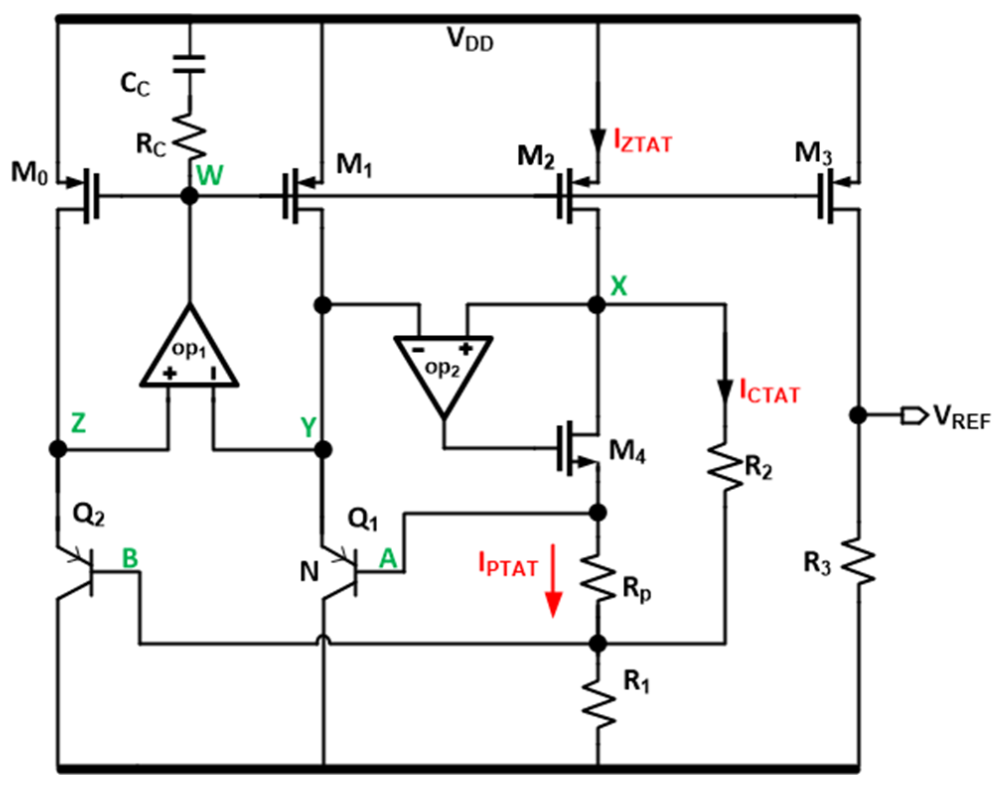
Figure 1 shows a conventional current-mode BGR. Q1, Q2, and
R1 form the BGR core cell, and the area of Q2 is
n times that of Q1 [
17]. The operational amplifier (op1) modulates the current through the BJT so that the potentials at nodes X and Y are equal, and the current density difference in Q1 and Q2 causes the voltage across
R1 to have PTAT behaviour. The current through
R1,
R2 can be expressed as
The output current through M2 is the sum of I
R1 and I
R2. The CTAT current has a TC of −2 mV/°C and a PTAT of 25 µV (for
n = 24). Therefore, we need to amplify the PTAT currents so that TC is zero after summing. The output voltage can be expressed as shown in (3) [
17].
By adjusting the ratio of
R2 and
R1 to minimise TC and adjusting
RL to generate the desired output voltage. This CBGR is simple and provides an output voltage of less than 1 V, but it has some problems. The
R2 required for zero TC is very large. For example, to bias the BG core to 3 µA, the values of
R1 and
R2 should be 17 kΩ and 198 kΩ, respectively. Such a large value of
R2 occupies a lot of active space, and there are also two instances of
R2, and, hence, this is an area-in-efficient [
4,
17]. Conventionally, the VBGR has two operating points, a desired and an undesired operating point (zero current). Therefore, a start-up circuit prevents the circuit from getting stuck at zero current. In contrast, CBGR has multiple operating points. This is because when the bandgap core carries little current, Q
1 Q
2 will not turn on, and most of the current will flow through
R2 (
Figure 1). Therefore, op
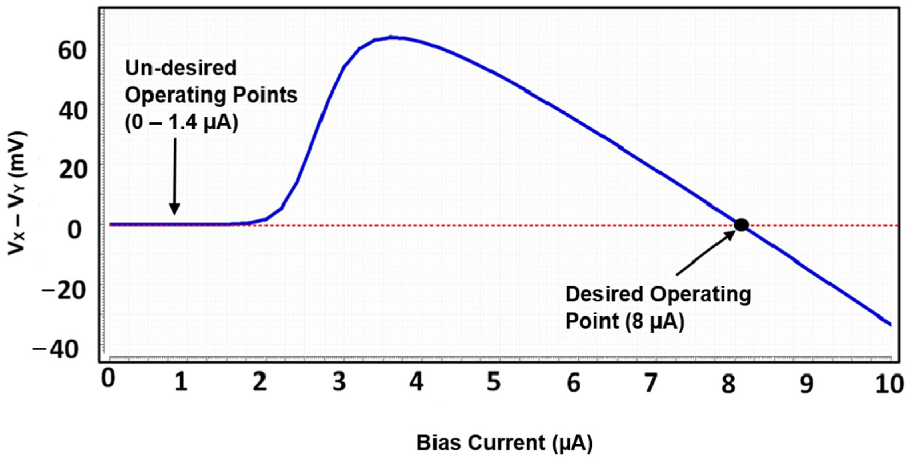
1 opamp will sense zero differential voltage until the current is large enough to turn on the BJT. To quantify the operating point, replace M
0 and M
1 with ideal current sources, you must sweep their values from 0 to 10 µA, and plot the differential input voltage of the opamp as in
Figure 2. At a maximum bias current of 1.4 µA, the opamp input terminals will see the same voltage (meaning the BJT is not turned on), indicating that the BGR can operate at any current within 1.4 µA (some undesirable points). When the current exceeds 1.4 µA, the Q1–2 device turns on, and the voltages of nodes X, Y are different for the same current. As soon as the current approaches 8 µA, the opamp op
1 input becomes 0 V again, so this is also the operating point (preferred). To avoid these problems, a starter circuit is necessary, and designing the starter circuit is difficult due to the above-mentioned points. It uses a POR circuit to avoid the failure of this circuit [
18]. A small asymmetry in the opamp is used, as shown in Equation (3) (intentionally adding a mismatch to
R2) [
11]. This circuit does not have access to the PTAT current like the VBGR circuit, so if PTAT is required, it must be generated by additional circuitry at the cost of more current and mismatch, as given in Equation (4). This architecture also amplifies that there is opamp offset with a large gain compared to the traditional BGR due to the resistor loaded on the input terminal of the opamp. Therefore, a larger gain will amplify any residual input-related offset and affect the output TC. Equations (4) and (5) show the output voltage due to only the opamp offset in VBGR and current-mode BGR, respectively [
17].
According to the authors, the bandgap core is of a low current and symmetrical, which causes the circuit to stall at some operating point. Therefore, removing
R2 makes the circuit asymmetrical at all currents and reduces the loading of
R2 on the opamp input. Therefore, removing
R2 minimises the number of operating points. The main purpose of
R2 is to eliminate multi-operating points and ensure only two operating points [
17].
3. Proposed Technique
Figure 3 shows the proposed architecture circuit, which consists of two sections. One is a BGR core that generates a PTAT stream consisting of Q
1, Q
2, OP1, M
0, M
1,
Rp, and the other is a stream adder consisting of OP
2, M
4, and
R2. Note that the start circuit is not shown here for simplicity. Compared to the conventional VBGR, this proposal uses the base connection to generate the PTAT current, thus achieving a kind of curvature compensation [
11]. Since the voltage across R
P is V
BE2–V
BE1, it has a PTAT characteristic. The operational amplifier (OP
2) sets the gate voltage of M4 such that V
X = V
Y. Therefore, the voltage across
R2 will be VBE2, and the current through
R2 will have the properties of CTAT. M
2 carries a sum of PTAT and CTAT currents that allows the TC to be set to zero by adjusting the ratio of
R2 and
Rp. The output voltage is given using Equation (6).
where Vos is the OP
1 offset.
Resistor
R1 is not required in this circuit, but its voltage has a non-linear temperature dependence due to the base current, which improves TC. However,
R1 increases the minimum power supply required by the circuit, so VR1 < 30 mV for this current research. Even at very low bias currents, the opamp input nodes experience different impedances, so there is no unwanted operating point other than zero current. This is a major advantage of the proposed BGR compared to CBGR. The new proposed circuit has a smaller silicon area than the CBGR (up to 29% savings in silicon area), as only one CTAT register is used. Since
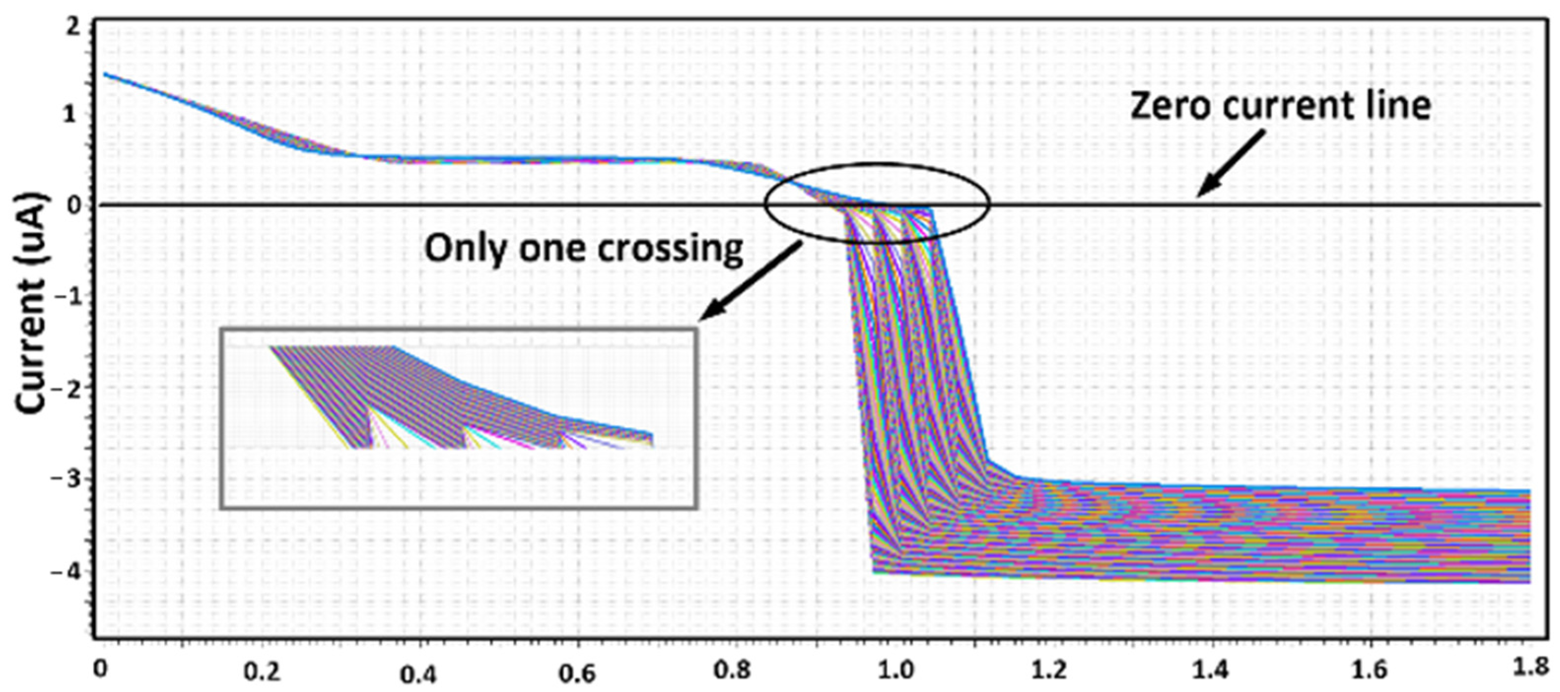
R2 does not load the OP1 input, the opamp offset voltage is amplified by the gain, given in Equation (4), which is less than the current-mode BGR. A voltage source was connected to the opamp output (node w), shifted its value from 0 to Vdd, and plotted the current through the voltage source to show the number of operating points. The number of current zero crossing points indicates the number of operating points.
Figure 4 shows the current through the voltage source added in the testbench. Since there is only one crossing point in 200 Monte Carlo simulations, this new proposal circuit successfully eliminates all unnecessary operating points (because of the start-up circuit; thus, there is no zero current point).
4. Self-Bias Opamp and Design Techniques
The systematic offset of OP1 plays a significant role in BGR performance with respect to temperature [
19,
20]. Equation (6) shows that VOS is amplified using a ratio of
due to the closed-loop nature of the BGR, and this amplification factor is so large that it might impact the TC of the output voltage. Unfortunately, the opamp offset temperature sensitivity is unknown; otherwise, it could be corrected similarly to the output voltage. If the opamp tail current was biased with the constant current, then the opamp output common-mode voltage will have a different nature than the bandgap PMOS current sources. One way to reduce/solve this problem is to bias the opamp with the BGR core current [
21,
22]. This gives the current mirror gain because the opamp output matches the desired output voltage (vdd-vsg, p). The ratio will be close to one.
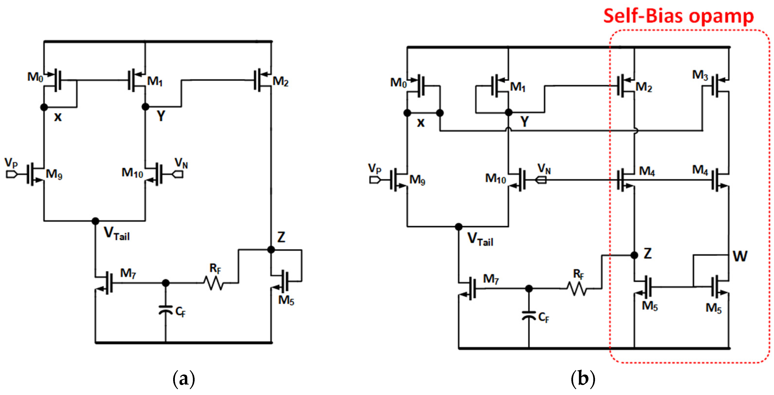
Figure 5a shows the conventional self-bias scheme, which works as follows. M
0, M
1, M
7, M
9, M
10 form the current source load opamp. The node Y voltage has been sensed with M
2 and M
5 and drives the opamp tail current source gate with a low pass filter. The low pass filter is an essential part of the self-bias as it will slow down the self-bias loop such that for the main BGR loop, the opamp current is a static parameter. The loop gain of the self-bias depends on the ratio of
gm2 and
m5. The main purpose of the self-bias loop is to make the x,y node potential as close as possible. Unfortunately, due to the limited gain in the self-bias loop, they will be better than the fixed bias opamp, but still, there is room for improvement.
Figure 5b depicts the proposed opamp bias structure, where the gain from node x,y to node z has been increased significantly. An opamp has been deployed from nodes x,y to node z to considerably enhance loop gain, reducing the steady state error between the node x,y potentials. The loop gain can be expressed as follows (7). The loop gain has dominated the pole associated with the low pass RC filter, which keeps the other opamp poles far away, such that the phase margin is close to 90° (this phase margin differs from the main loop). Compared to
Figure 5a, this circuit loop gain is almost 30 dB higher (higher than
).
The often VDS mismatch of the self-bias will have minor errors in the final settling. Hence, the M4 device has been introduced to match the bias network VDS to the main opamp.
5. Simulation Results
The proposed BGR was implemented in TSMC 28 nm low-power (LP) CMOS technology, which has 10 metals and one poly layer. A low-power process means there is very little leakage current in the off state of the transistor; hence, the threshold voltage of the transistor would be a little higher [
23]. This process contains core and IO transistors to support low- and high-voltage supply. Post-layout simulations based on a resistor coupling capacitor-extracted netlist were performed across NMOS and PMOS typical, NMOS and PMOS fast, NMOS and PMOS slow, fast NMOS and slow PMOS, and slow NMOS and fast PMOS corners. Also, the simulations assumed the PAD capacitance and parasitic interface while connected to the PCB. BGR draws 31.23 µA from the 1.05 V supply.
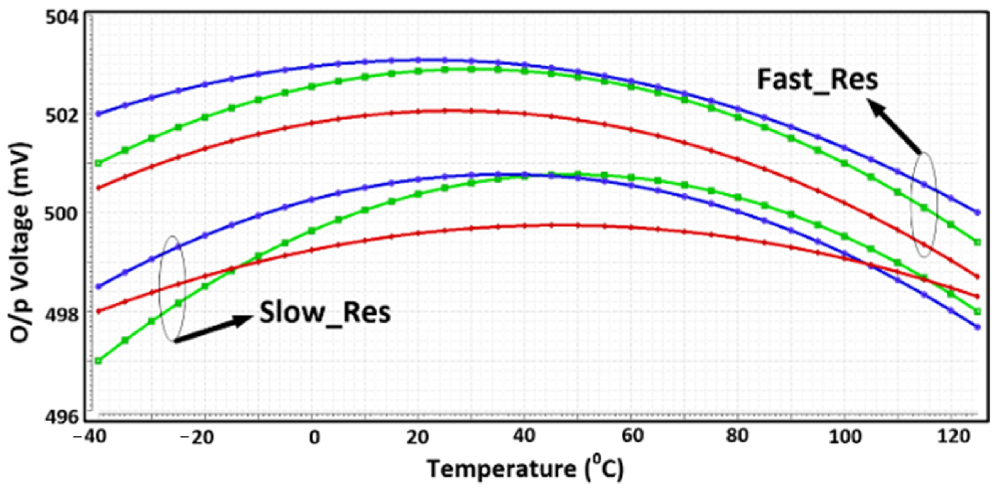
Figure 6 shows the output voltage versus temperature for process corners (TT, FF, SS) and resistance corners (high and low). The output voltage varies from 496.8 to 503 mV over the industrial temperature range (−40 °C to 125 °C) with a TC of 10.5 ppm/0 °C at the FF corner. An interesting observation is that the output voltage is more sensitive to the resistance corner than the MOS corner at a given temperature because the bias current in the BGR core is proportional to RP, which will be changed [
23]. Therefore, two sets of output plots in
Figure 6 correspond to the resistance corners.
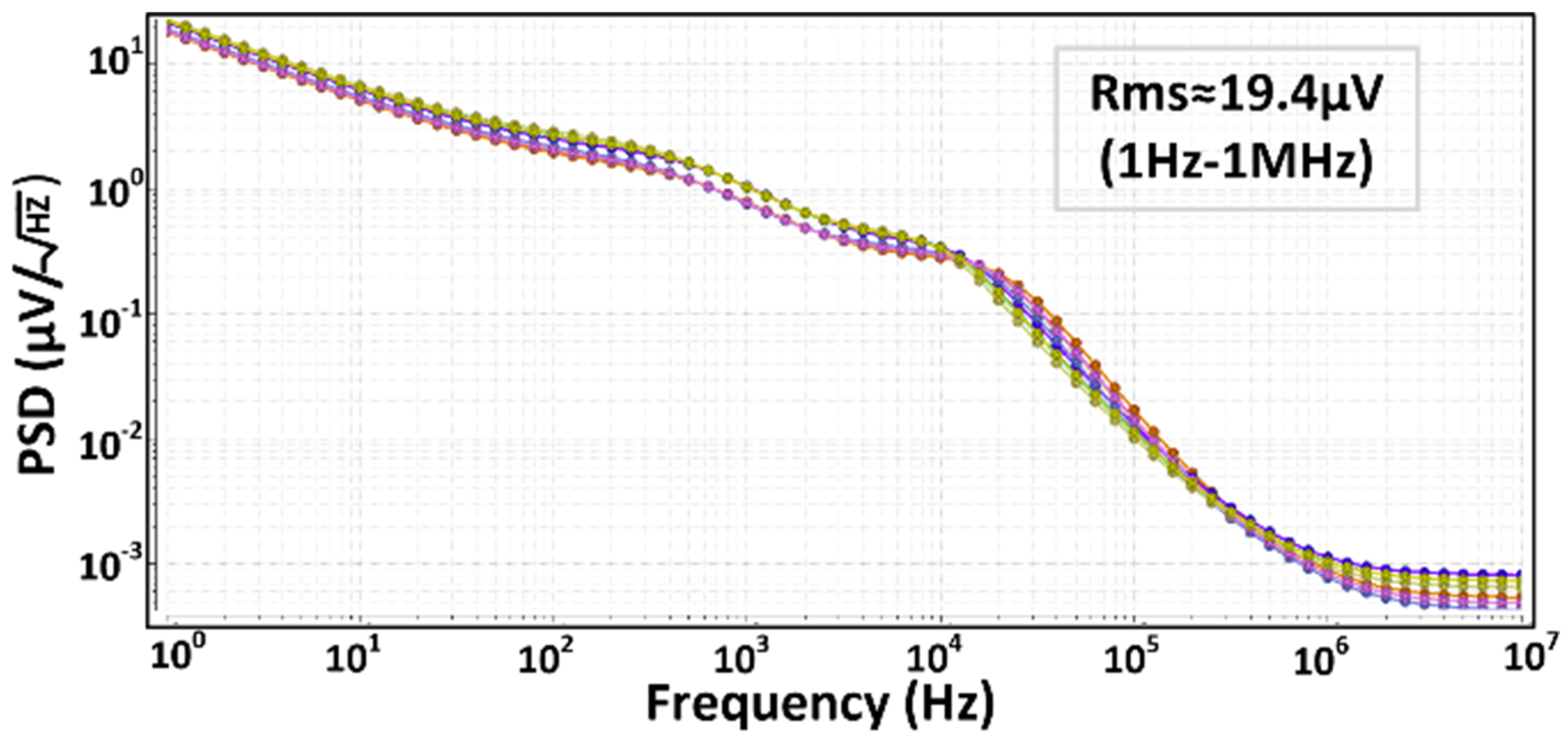
Figure 7 shows the output’s simulated noise power spectral density and the integrated RMS noise of ~19.4 μV. Most of the noise is contributed by OP1, Rp, and M0. More importantly, the noise in OP1 is multiplied with R1/Rp. This was reduced by choosing a higher n so that there is less of the multiplication factor, but the trade-off with a very high n increases the risk of the reverse saturation current.
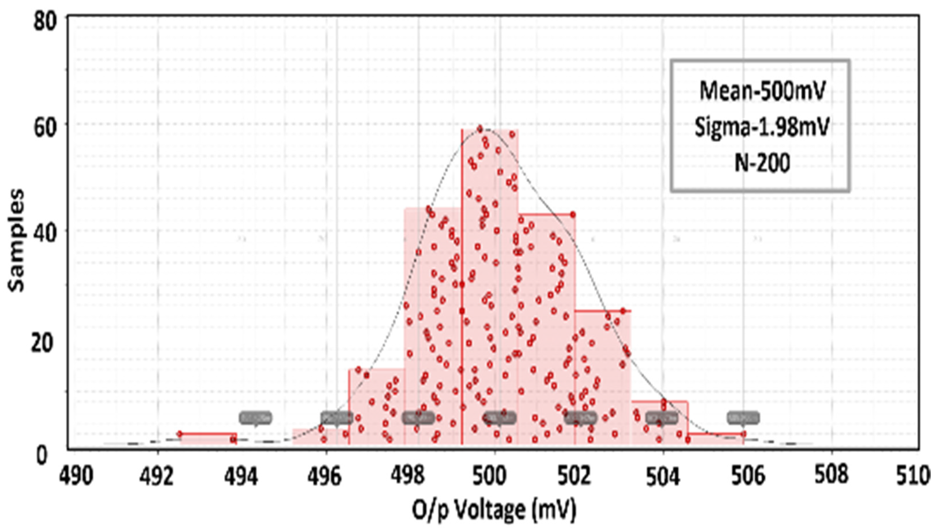
Figure 8 shows a simulated histogram of the output voltages corresponding to 6-Sigma 200 Monte Carlo simulations [
24], indicating a standard deviation of 1.98 mV and an accuracy of 1.21%. Note each point in the histogram is a single Monte Carlo simulation.
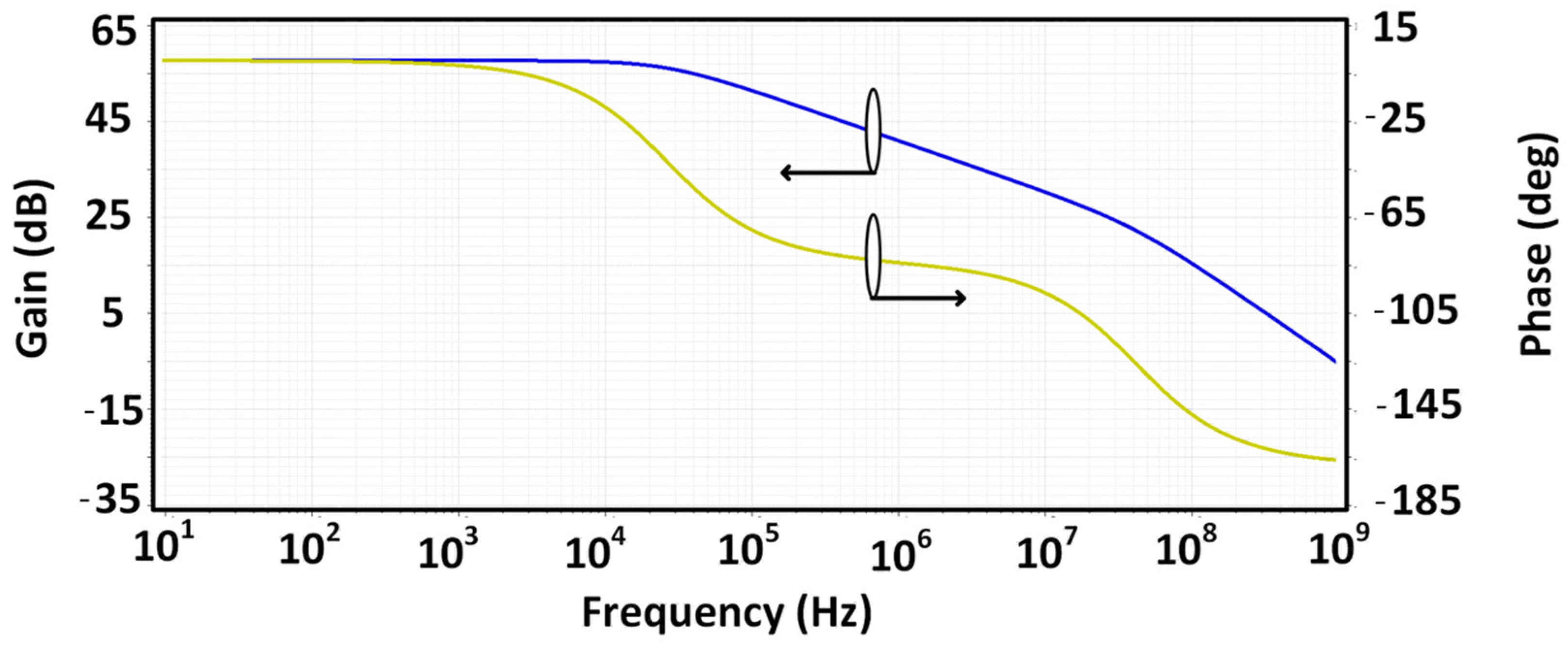
Figure 9 shows the simulated gain and phase of the proposed self-bias opamp [
25].
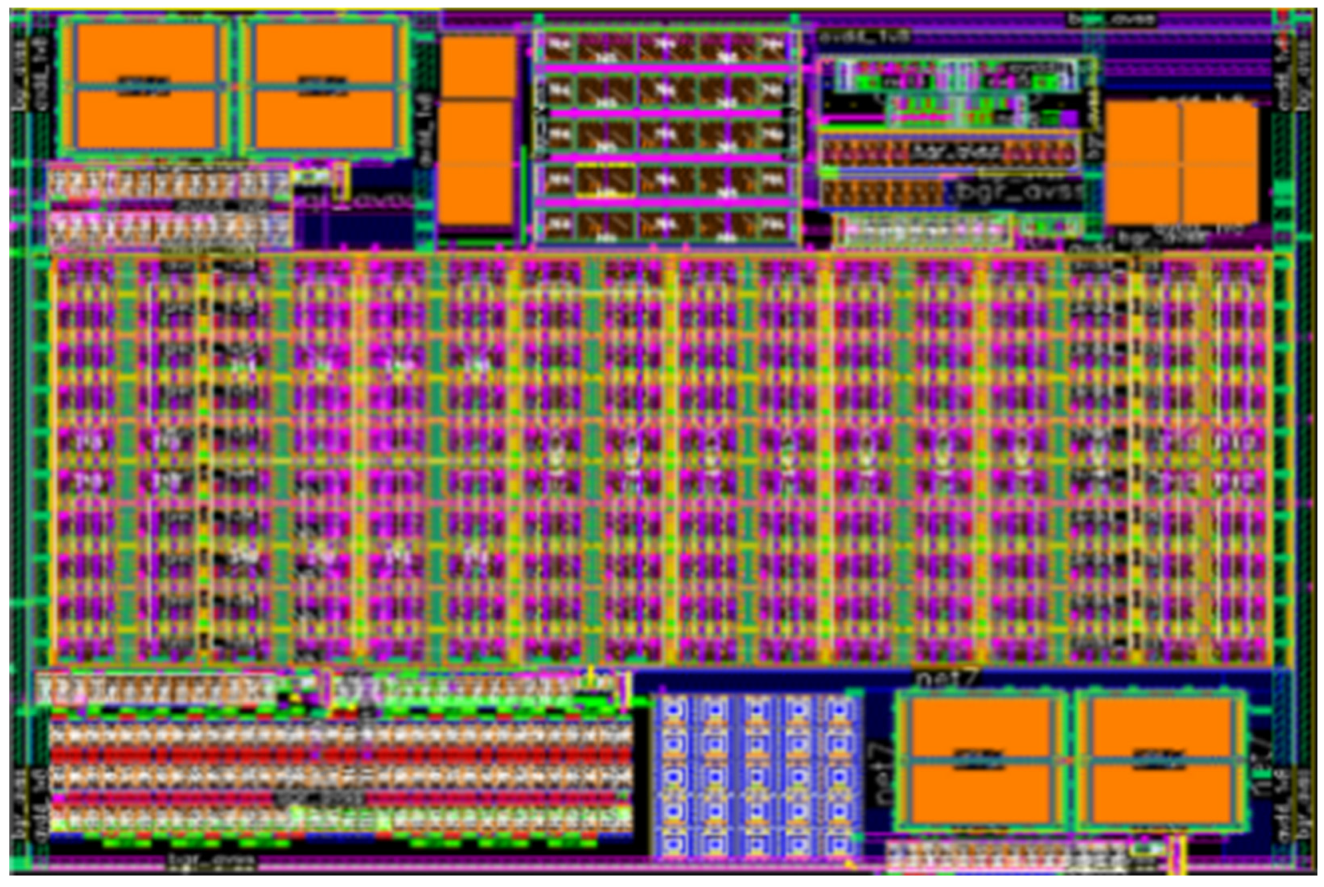
Figure 10 shows the layout of the proposed circuit. It has a surface area of 81 × 42 µm
2, including decoupling capacitors and dummy devices, most of which are dominated by the current source OPAMP (OP1) and PMOS [
26,
27,
28]. The proposed design has a lower temperature coefficient compared to the designs by Yu and L. Siek [
7], A. J. Annema [
12], and Yu and J. Lee [
29], as shown in
Table 1.
A. J. Annema [
12] reached a lower supply voltage (0.15 V less) and power consumption (38.4% less) compared to the proposed work. However, this came at a much higher temperature coefficient (95.2 times more) and generated 3.04 times more noise. The design by Yu and L. Siek [
7] generated less noise compared to the proposed design but came at the cost of a higher supply voltage (0.75 V), higher temperature coefficient (2.5 ppm/°C), and consumed 3.01 times more power.
Lastly, the design by J. Lee [
29,
30] underperformed compared to the proposed design in terms of the supply voltage (0.375 V more needed), temperature coefficient (3.9 times more), and power (1.7 times more), as shown in
Table 1. This layout was designed for the sake of extracted simulations, not for manufacturing. Hence, we did not include pads/bumps or package-related parasitic elements [
31,
32,
33,
34].


