
Input Voltage-Level Driven Split-Input Inverter Level Shifter for Nanoscale Applications
 , , and
Abstract
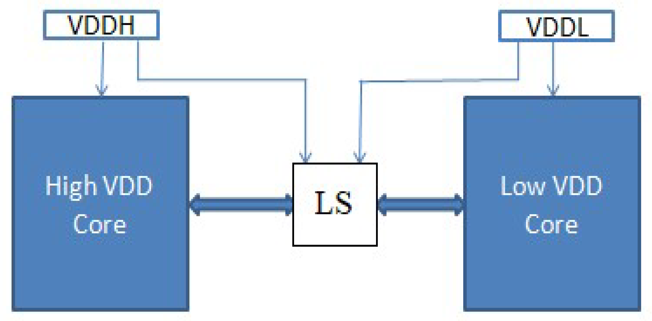
1. Introduction
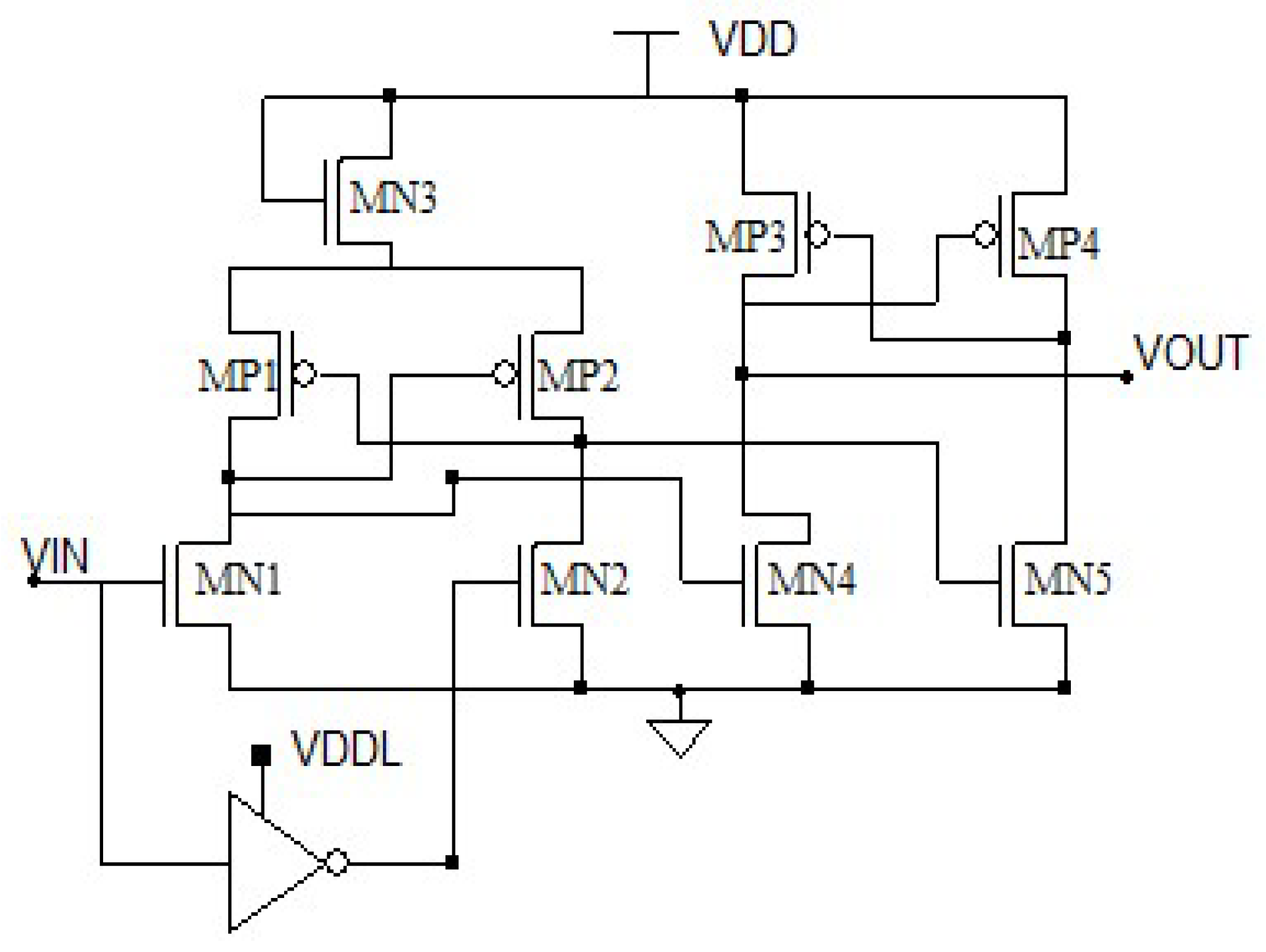
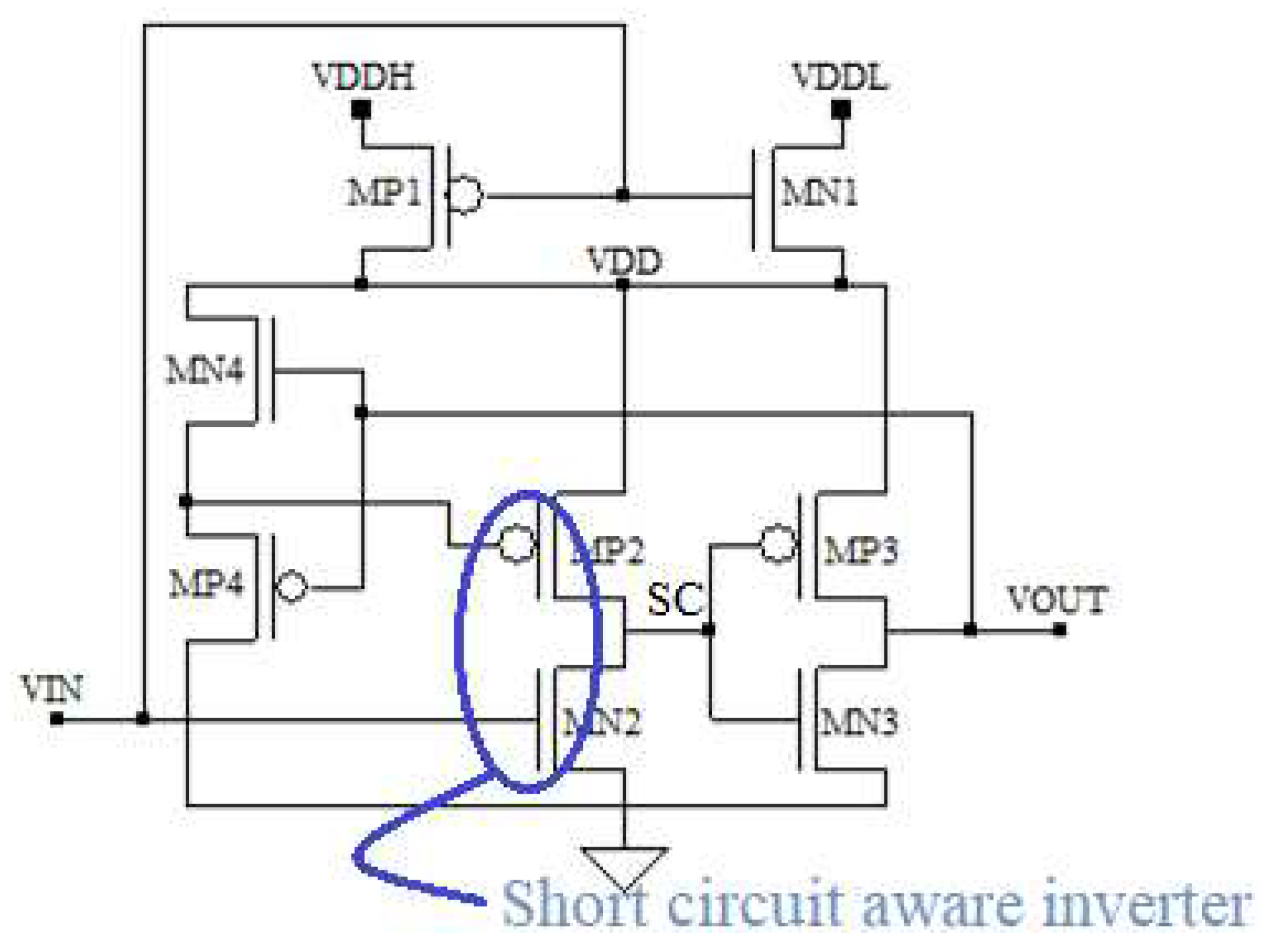
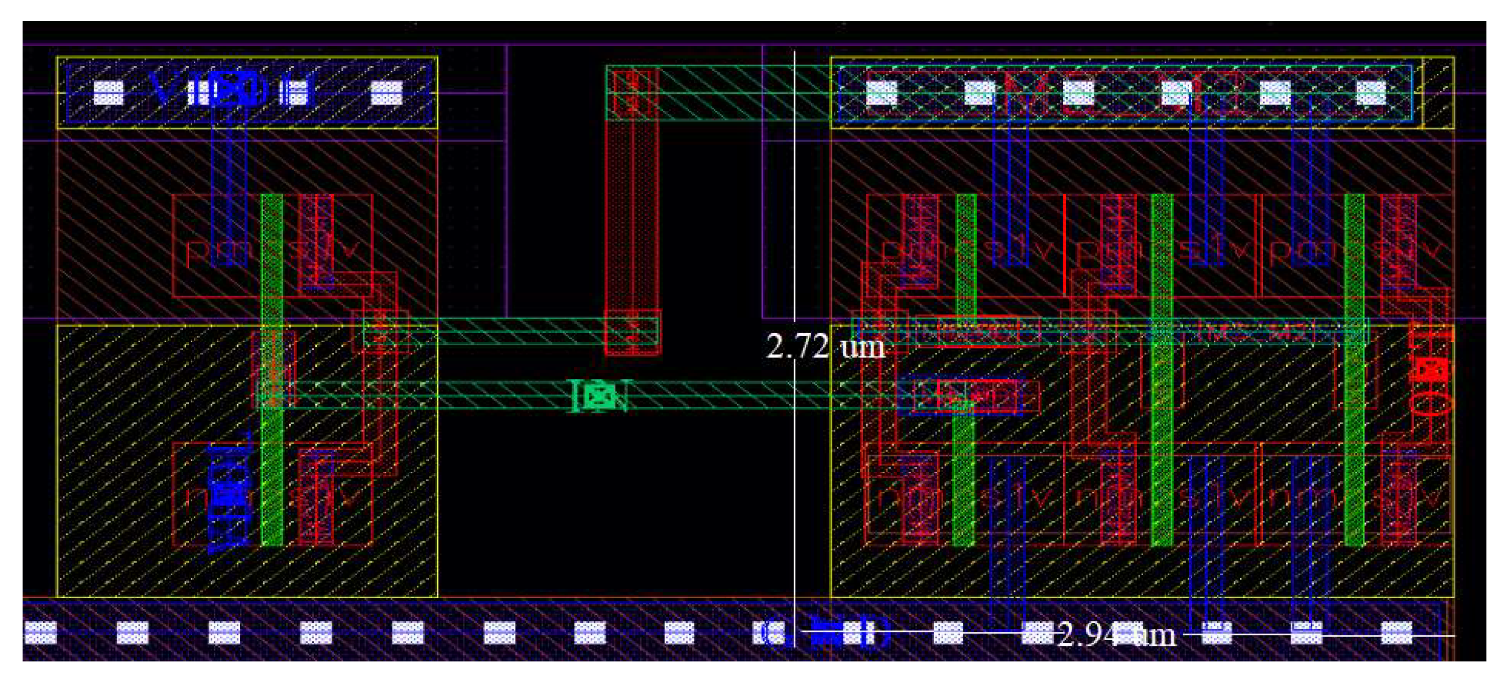
2. Proposed Input Voltage-Level Driven Split-Input Inverter Level Shifter
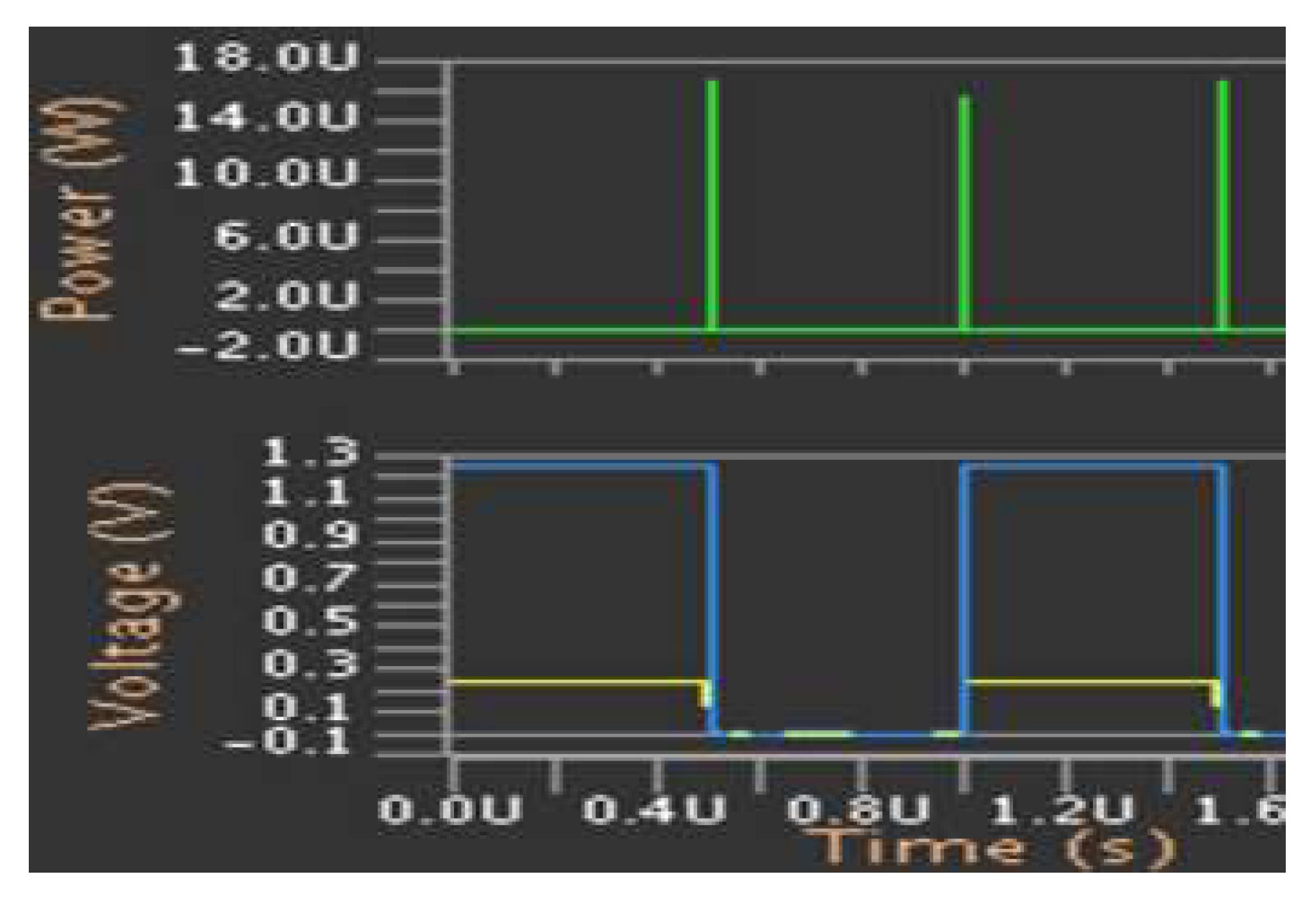
3. Measurement and Results
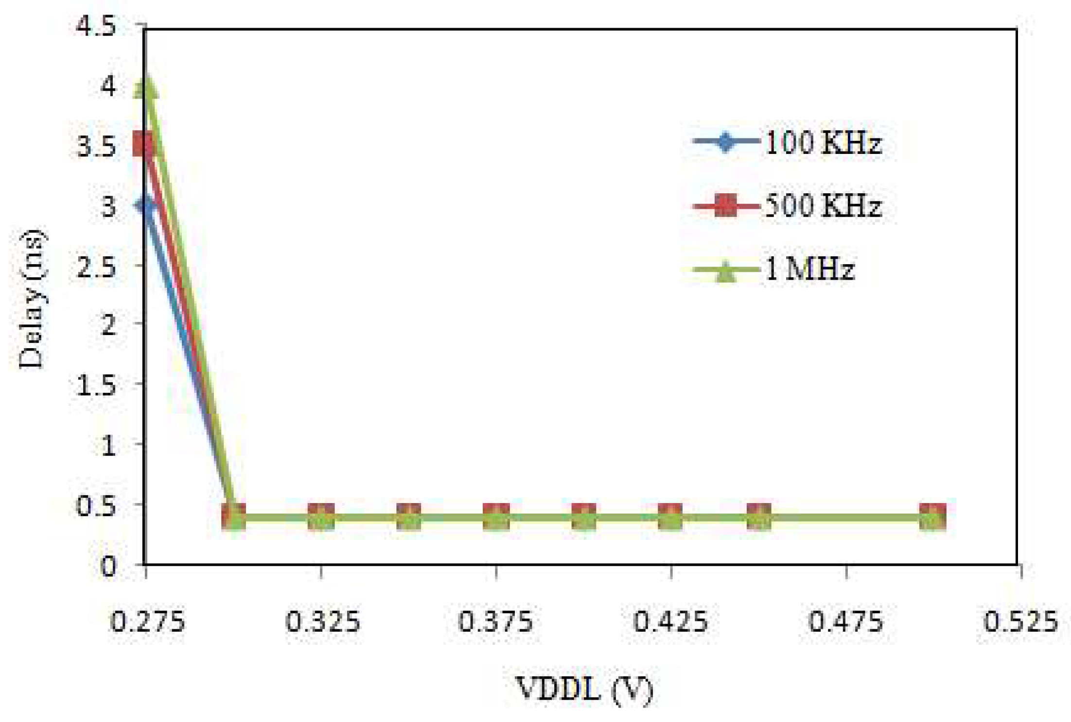
3.1. Power and Delay as Functions of VDDL
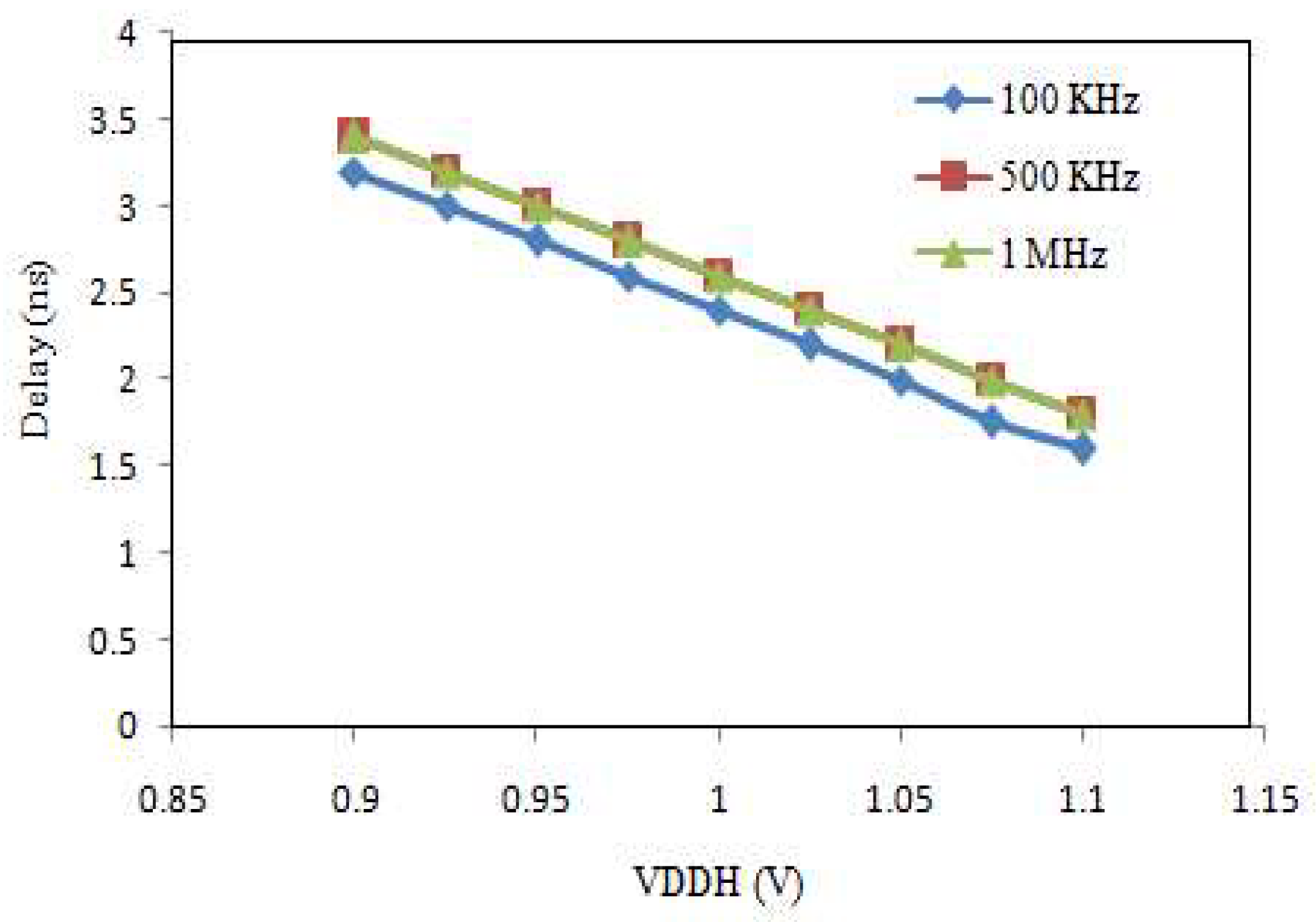
3.2. Power and Delay as Functions of VDDH
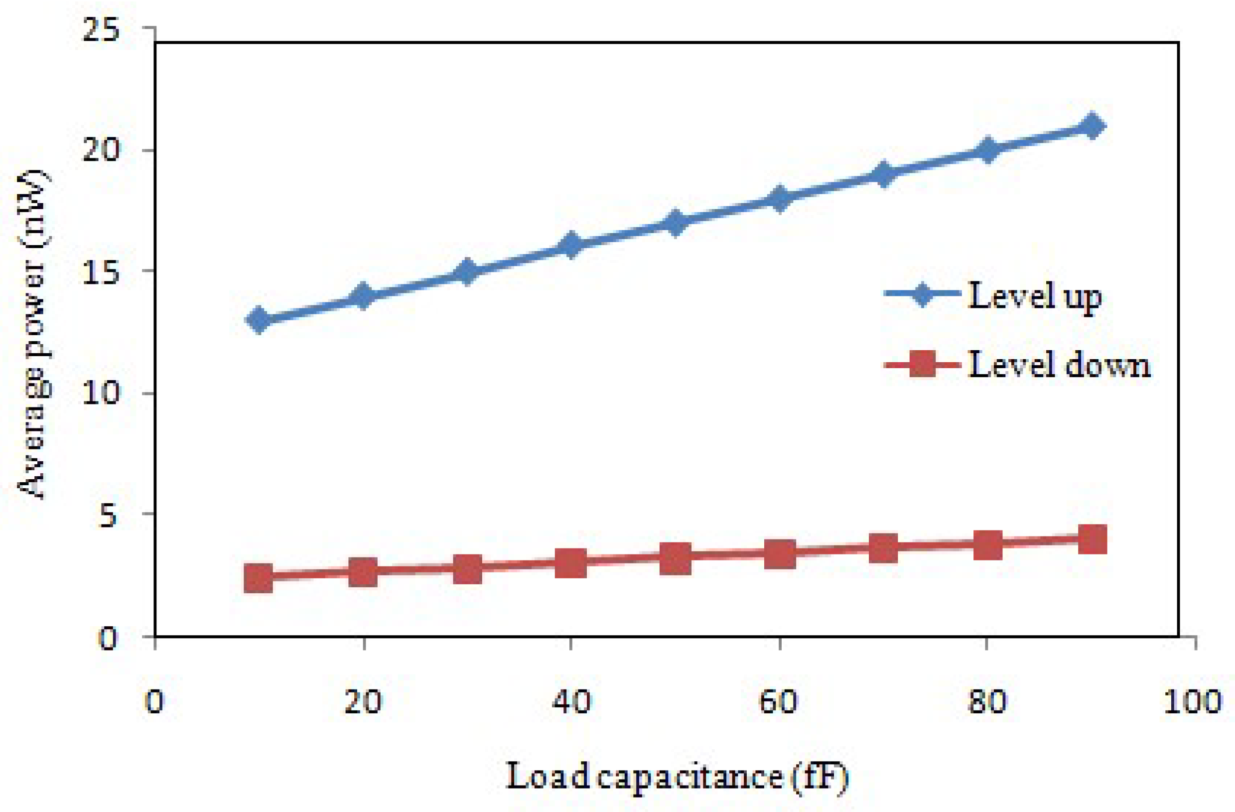
3.3. Impact of Load on SILS Performance
3.4. Comparison Results and Discussion
4. Conclusions
Author Contributions
Funding
Data Availability Statement
Conflicts of Interest
References
- Saleh, R. System-on-chip: Reuse and integration. Proc. IEEE 2006, 94, 1050–1069. [Google Scholar] [CrossRef]
- Lanuzza, M.; Perri, S. Fast and wide range voltage conversion in multisupply voltage designs. IEEE Trans. Very Large Scale Integr. Syst. 2015, 23, 388–391. [Google Scholar] [CrossRef]
- Zhao, W.; Alvarez, A.B.; Ha, Y. A 65-nm 25.1-ns 30.7-fJ robust subthreshold level shifter with wide conversion range. IEEE Trans. Circuits Syst. II Express Briefs 2015, 62, 671–675. [Google Scholar] [CrossRef]
- Lanuzza, M.; Crupi, F.; Rao, S.; De Rose, R.; Strangio, S.; Iannaccone, G. An ultralow-voltage energy-efficient level shifter. IEEE Trans. Circuits Syst. II Express Briefs 2017, 64, 61–65. [Google Scholar] [CrossRef]
- Mocan, B.; Osan, C.; Fulea, M.; Chis, I.A.; Timoftei, S.; Sarb, A. An Integrated Model for Solving Cell Formation Problem and Robot Scheduling using Timed Petri Nets. In Proceedings of the 2016 International Conference on Production Research—Africa, Europe and the Middle East and 4th International Conference on Quality and Innovation in Engineering and Management, Cluj-Napoca, Romania, 25–30 July 2016; pp. 91–96. [Google Scholar]
- Fassio, L.; Settino, F.; Lin, L.; De Rose, R.; Lanuzza, M.; Crupi, F.; Alioto, M. A robust, high-speed and energy-efficient ultralow voltage level shifter. IEEE Trans. Circuits Syst. II Express Briefs 2021, 68, 1393–1397. [Google Scholar] [CrossRef]
- Låte, E.; Ytterdal, T.; Aunet, S. An energy efficient level shifter capable of logic conversion from sub-15 mV to 1.2 V. IEEE Trans. Circuits Syst. II Express Briefs 2020, 67, 2687–2691. [Google Scholar] [CrossRef]
- Cao, L.; Bale, S.J.; Trefzer, M.A. Multi-objective digital design optimization via improved drive granularity standard cells. IEEE Trans. Circuits Syst. I Regul. Pap. 2021, 68, 4660–4671. [Google Scholar] [CrossRef]
- Rajendran, S.; Chakrapani, A. A 16 ns, 28 fJ wide-range subthreshold level converter using low-voltage current mirror. Circuits Syst. Signal Process. 2020, 40, 1479–1495. [Google Scholar] [CrossRef]
- Matsuzuka, R.; Hirose, T.; Shizuku, Y.; Shinonaga, K.; Kuroki, N.; Numa, M. An 80-mV-to-1.8-V conversion-range low-energy level shifter for extremely low-voltage VLSIs. IEEE Trans. Circuits Syst. I Regul. Pap. 2017, 64, 2026–2035. [Google Scholar] [CrossRef]
- Zhou, J.; Wang, C.; Liu, X.; Zhang, X.; Je, M. An ultra-low voltage level shifter using revised wilson current mirror for fast and energy-efficient wide-range voltage conversion from sub-threshold to I/O voltage. IEEE Trans. Circuits Syst. I Regul. Pap. 2015, 62, 697–706. [Google Scholar] [CrossRef]
- Kabirpour, S.; Jalali, M. A power-delay and area efficient voltage level shifter based on a reflected-output Wilson current mirror level shifter. IEEE Trans. Circuits Syst. II Express Briefs 2020, 67, 250–254. [Google Scholar] [CrossRef]
- Basha, M.M.; Gundala, S.; Khan, S.I. Design of energy and EDP efficient 1-bit full subtractor based divider circuits for computing systems. Int. J. Syst. Syst. Eng. 2021, 11, 257–267. [Google Scholar] [CrossRef]
- Ma, C.; Ji, Y.; Qiao, C.; Zhou, T.; Qi, L.; Li, Y. An energy-efficient level shifter using time borrowing technique for ultra wide voltage conversion from sub-200 mV to 3.0 V. In Proceedings of the 2021 IEEE International Symposium on Circuits and Systems (ISCAS), Daegu, Republic of Korea, 22–28 May 2021; pp. 1–5. [Google Scholar]
- Neeraj, K.; Mahaboob Basha, M.; Gundala, S. Design of low power SRAM-based ubiquitous sensor for wireless body area networks. Int. J. Pervasive Comput. Commun. 2021, 17, 611–621. [Google Scholar] [CrossRef]
- Yuan, B.; Xiao, L.Q.; Wang, B.Y.; Ying, J. High-speed dynamic level shifter for high-side bootstrapped gate driver in high-voltage buck regulators. IEEE Trans. Circuits Syst. II Express Briefs 2021, 68, 3083–3087. [Google Scholar] [CrossRef]
- Sarmiento, M.; Nguyen, K.D.; Duran, C.; Hoang, T.T.; Serrano, R.; Hoang, V.P.; Tran, X.T.; Ishibashi, K.; Pham, C.K. A sub-µW reversed-body-bias 8-bit processor on 65-nm silicon-on-thin-box (SOTB) for IoT applications. IEEE Trans. Circuits Syst. II Express Briefs 2021, 68, 3182–3186. [Google Scholar]
- Gundala, S.; Basha, M.M.; Vijayakumar, S. Level-Up/Level-Down Voltage Level Shifter for Nano-Scale Applications. J. Eng. Sci. Technol. 2022, 17, 745–759. [Google Scholar]
- Sudhakar, M.V.; Stan, O.P. Implementation of High-Speed Compact Level-Up Shifter for Nano-Scale Applications. Electronics 2023, 12, 5015. [Google Scholar] [CrossRef]
- Lütkemeier, S.; Rückert, U. A subthreshold to above-threshold level shifter comprising a Wilson current mirror. IEEE Trans. Circuits Syst. II Express Briefs 2010, 57, 721–724. [Google Scholar] [CrossRef]
- Le, V.L.; Kim, T.T.-H. An area and energy efficient ultra-low voltage level shifter with pass transistor and reduced-swing output buffer in 65-nm CMOS. IEEE Trans. Circuits Syst. II Express Briefs 2018, 65, 607–611. [Google Scholar] [CrossRef]
- Jeong, H.; Kim, T.H.; Park, C.N.; Kim, H.; Song, T.; Jung, S.O. A wide-range static current-free current mirror-based LS with logic error detection for near-threshold operation. IEEE J. Solid-State Circuits 2021, 56, 554–565. [Google Scholar] [CrossRef]
- Truesdell, D.S.; Calhoun, B.H. A single-supply 6-transistor voltage level converter design reaching 8.18-fJ/transition at 0.3–1.2-V range or 44-fW leakage at 0.8–2.5-V range. IEEE Solid-State Circuits Lett. 2007, 3, 502–505. [Google Scholar] [CrossRef]


| Ref./ Proposed | Technology (nm) | Type of Technique | VDDL (V) | VDDH (V) | Power (nW) | Delay (ns) | PDP (fJ) |
|---|---|---|---|---|---|---|---|
| [3] | 65 | CC | 0.3 | 1.2 | 30.7 | 25 | 0.768 |
| [4] | 55 | CC | 0.3 | 1.2 | 23 | 53 | 1.219 |
| [20] | 65 | CM | 0.3 | 1.2 | 552 | 17.5 | 9.660 |
| [11] | 55 | CM | 0.3 | 1.2 | 27 | 82 | 2.214 |
| [21] | 65 | CM | 0.3 | 1.2 | 124 | 7.5 | 0.930 |
| [22] | 55 | CM | 0.45 | 1.2 | 180 | 57 | 10.26 |
| [23] | 65 | DLS | 0.3 | 1.2 | 12 | 186 | 2.230 |
| SILS (Up/Down) | 65 | Inverter | 0.2 | 1.2 | 16 | 0.4 | 0.006 |
| 03 | 1.75 | 0.005 |
Disclaimer/Publisher’s Note: The statements, opinions and data contained in all publications are solely those of the individual author(s) and contributor(s) and not of MDPI and/or the editor(s). MDPI and/or the editor(s) disclaim responsibility for any injury to people or property resulting from any ideas, methods, instructions or products referred to in the content. |
© 2024 by the authors. Licensee MDPI, Basel, Switzerland. This article is an open access article distributed under the terms and conditions of the Creative Commons Attribution (CC BY) license (https://creativecommons.org/licenses/by/4.0/).
Share and Cite
Gundala, S.; Basha, M.M.; Madhurima, V.; Stan, O.P. Input Voltage-Level Driven Split-Input Inverter Level Shifter for Nanoscale Applications. Electronics 2024, 13, 1115. https://doi.org/10.3390/electronics13061115
Gundala S, Basha MM, Madhurima V, Stan OP. Input Voltage-Level Driven Split-Input Inverter Level Shifter for Nanoscale Applications. Electronics. 2024; 13(6):1115. https://doi.org/10.3390/electronics13061115
Chicago/Turabian StyleGundala, Srinivasulu, Mohammed Mahaboob Basha, Virupakshi Madhurima, and Ovidiu Petru Stan. 2024. "Input Voltage-Level Driven Split-Input Inverter Level Shifter for Nanoscale Applications" Electronics 13, no. 6: 1115. https://doi.org/10.3390/electronics13061115
APA StyleGundala, S., Basha, M. M., Madhurima, V., & Stan, O. P. (2024). Input Voltage-Level Driven Split-Input Inverter Level Shifter for Nanoscale Applications. Electronics, 13(6), 1115. https://doi.org/10.3390/electronics13061115