Communication

A 0.5 V Nanowatt Biquadratic Low-Pass Filter with Tunable Quality Factor for Electronic Cochlea Applications

Faculty of Electronics Telecommunications and Informatics, Gdańsk University of Technology, 80-233 Gdańsk, Poland
*
Author to whom correspondence should be addressed.
Electronics 2024, 13(2), 399; https://doi.org/10.3390/electronics13020399
Submission received: 21 December 2023 / Revised: 15 January 2024 / Accepted: 16 January 2024 / Published: 18 January 2024
(This article belongs to the Special Issue Design of Low-Voltage and Low-Power Integrated Circuits)

Abstract

:
A novel implementation of an analogue low-power, second-order, low-pass filter with tunable quality factor (Q) is presented and discussed. The filter feature is a relatively simple, buffer-based, circuit network consisting of eleven transistors operating in a subthreshold region. Q tuning is accomplished by injecting direct current into a network node, which changes the output resistance of the transistors and, as a result, modifies the filter network’s loss, and thus its Q. Q tuning is independent of a filter cut-off frequency (ω0). The filter, with a nominal ω0 of 1 kHz, was fabricated using a 0.18 µm CMOS technology, and features a Q range of 2–11, power consumption of up to 52 nW, and a 59 dB dynamic range when using a 0.5 V supply. The ω0 can be tuned from 0.5 to 2.5 kHz using a traditional method by changing the transistor transconductances, but this process partially affects the quality factor.

1. Introduction

One important functional block that is a part of hearing aids [1,2,3,4,5,6] as well as devices for human voice recognition [7], are tunable filters [8,9,10,11] that emulate characteristics of a human cochlea. Such filters allow pre-processing of acoustic signals based on extracting components of the amplitude spectrum of the received sounds and enabling adaptive adjustment of the sensitivity of the signal path in individual frequency bands. Such properties of the filters enable high dynamics and the intelligibility of received sounds, especially human speech, in the presence of noise and external interference, which has a significant impact on the comfort of using a hearing aid and the correctness of human speech recognition. Nowadays, hearing aids are more often manufactured in the form of implants that are placed in the middle ear of hearing-impaired people. In such a case, the problem of reducing power consumption and the voltage supplying the implant becomes particularly important, as the implant itself contains a small store of electrical energy, and its long-term operation relies on the cyclic recharging of energy [6].
Analogue filter implementations (e.g., as in [12,13,14,15,16,17,18]) show that analogue filters are more advantageous than fully digital ones from a power reduction perspective. On the other hand, examples of analogue filters realized so far show that it is still difficult to achieve sufficient performance, especially regarding low power consumption, to allow cochlear implant operation without energy charging for many hours. As a result, new, more efficient filter implementations with more favourable parameters are still being researched. Experience from previous implementations of filters in CMOS technology has demonstrated that satisfactory results can be achieved using banks of parallel- [12,13,14] or cascade- [15,16,17,18] connected second-order low-pass filters with electronically tunable quality factor (Q).
Cochlear filter banks typically cover the entire acoustic bandwidth, 20 Hz to 20 kHz, which can be limited to the range of 250 Hz–8 kHz when implementing only the speech recognition function [19]. Coverage of the required bandwidth is achieved using the appropriate number of filters in a bank, with octave-distributed cut-off frequencies (ω0). As the volume of the received sound changes, adaptive adjustment of the acoustic sensitivity is realized by means of changes in the quality factor (Q) of individual filters, which is consistent with the physiology of human hearing [20].
The second-order filter presented in this paper was designed for use in cochlear filter banks. Thus, special attention was paid to voltage and power supply reduction and implementation of effective electronic tuning of the quality factor. MOS transistors operating in the subthreshold region with nano ampere bias currents were used to achieve a significant reduction in power consumption. The following sections of this paper describe the filter circuit, the theoretical analysis of the parameters, and measurement results obtained using a prototype filter fabricated using an X-FAB 180-nm CMOS process.

2. Materials and Methods

2.1. Principle of Operation
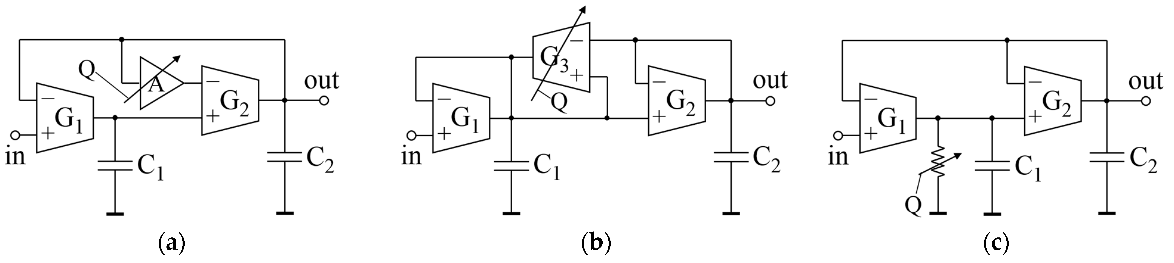
A detailed schematic of the proposed filter and its transconductance-C model are shown in Figure 1.
The filter consists of two transconductance stages. The first stage is a differential pair (M1, M2) loaded using a current mirror (M3, M4) and two extra current sources (M8, M9). Due to the low supply voltage (VDD) of 0.5 V, the bulk-driven differential pair is used. The second stage is a source follower (M5) loaded using a current source (M6). The stages are modelled using the transconductors G1 and G2 in Figure 1b. Their transconductances, G1 and G2, are determined by DC bias current IBIAS. The extra DC current IQ, generated by M8 and M9, modifies the resistance seen at node A and, as a result, also modifies the filter quality factor. Nodal resistance is modelled using the adjustable resistor R1 in Figure 1b.
With IBIAS and IQ less than 50 nA, all transistors in Figure 1a operate in the subthreshold region. The transistors’ gate transconductance (gm), back-gate transconductance (gmbs), and output conductance (gds) are proportional to their drain current (ID) according to the following relationships
g m I D n V t ,   g m b s n 1 n g m = n 1 I D n 2 V t , g d s I D λ D S
where Vt is the thermal voltage, and n and λDS are technology-dependent parameters [21,22].
Thus, the transconductances of the stages are
G 1 = g m b s 1 n 1 I B I A S 2 n 2 V t , G 2 = g m 5 I B I A S n V t ,
and the nodal resistance is
R 1 = 1 g d s 4 + g d s 9 + g d s 2 1 λ D S I D 4 + I D 9 + I D 2 = 1 λ D S I B I A S + 2 I Q
The resistance at node B, R2, can be neglected because it is connected in parallel to the resistance 1/G2, which is much smaller than R2; i.e., 1/G2 << R2. With this, the filter transmittance is
H s = V o u t s V i n s = A ω 0 2 s 2 + s ω 0 / Q + ω 0 2
where
A = 1 1 G 1 R 1 + 1 ,   ω 0 = G 1 + 1 / R 1 G 2 C 1 C 2 ,   Q = G 1 + 1 / R 1 G 2 C 1 C 2 R 1 1 + C 1 C 2 G 2 R 1
To tune the quality factor effectively, the sensitivity of the Q parameter with respect to R1 must be greater than the sensitivity of the other filter parameters. This is satisfied if C2 is much greater than C1, in details C2 >> C1G2R1 must be met, which is explained in the following section.

2.2. Q Tuning

Thus, assuming that C2 >> C1G2R1, the quality factor Formula (5) becomes
Q = C 2 > > C 1 G 2 R 1 G 1 + 1 / R 1 G 2 C 1 C 2 R 1 = ω 0 C 1 R 1
The relative sensitivities of the filter parameters with respect to R1 are
S R 1 A = 1 G 1 R 1 + 1 ,   S R 1 ω 0 = 1 2 G 1 R 1 + 1 ,   S R 1 Q = 1 1 2 G 1 R 1 + 1
where the relative sensitivity is defined as S x y = (dy/y)/(dx/x).
As G1R1 is much greater than one, G1R1 >> 1, and the sensitivity of Q to R1 is several times greater than other sensitivities; i.e., S R 1 Q >> S R 1 ω 0 and S R 1 Q >> S R 1 A . As a result, the quality factor adjustment only slightly disturbs the cut-off frequency and DC gain.
The condition C2 >> C1G2R1 at (6) is well satisfied in the developed filter, as C2 is 60 pF, C1 is 50 fF, and G2R1 ranges from 22 to 150.

2.3. ω0 Tuning

The cut-off frequency ω0 given by (5) is proportional to IBIAS, ω0 ~ IBIAS, which results from the facts that conductances G1, G2, and 1/R1 are ~IBIAS. Using the same facts in (6), it can be deduced that Q should vary moderately when IBIAS changes. The sensitivities of A, ω0, and Q with respect to IBIAS are as follows
S I B I A S A = 2 I Q I B I A S η + 1 + 2 I Q 0 ,       S I B I A S ω 0 = 1 I Q I B I A S η + 1 + 2 I Q 1 ,       S I B I A S Q = S I B I A S ω 0 I B I A S I B I A S + 2 I Q
where η = (n − 1)/(2n2VtλDS). When the typical parameters of the process are used (i.e., n ≈ 1.3, λDS ≈ 0.01 V−1, and Vt ≈ 25 mV), the η is about 350. Therefore, the sensitivity of ω0 to IBIAS is approximately equal to unity and is always greater than the sensitivity of Q to IBIAS.

2.4. Mismatch

Technological mismatch affects all filter components (and hence, filter parameters) according to general rules, and are not analysed in detail here. However, the mismatch related to components C1 and R1 requires some comment.
The small capacitor C1 is exposed to mismatch because of its small area (the Pelgrom rule) and the increased proportion of parasitic capacitances. Fortunately, the sensitivities of the filter parameters with respect to C1 do not depend on the value of C1: these sensitivities are constant and less than one; i.e., S C 1 ω 0 = −0.5, S C 1 Q = 0.5, and S C 1 A = 0. Thanks to this, the negative impact of a small C1 on the filter characteristic is reduced.
As S R 1 Q ≅ 1, deviations in R1 caused by mismatch directly translate into the spread of the quality factor. The mismatch in R1 may be relatively high, because R1 depends on many factors, such as transistor drain currents, channel lengths, λDS parameter, etc., which are sensitive to mismatch as well. However, detailed Monte Carlo simulations, taking into account all possible mismatch factors, show that ω0 spreads from 971 to 1023 Hz and Q varies from 21.15 to 21.9 dB, which means that the 1-sigma deviations in ω0 and Q are 7.95 Hz and 0.12 dB, respectively; i.e., only 0.8% and 0.5%, respectively, with respect to the mean values 0.99 kHz and 21.5 dB, as shown in Figure 2.

2.5. Noise

Figure 3a depicts the noise model of the filter. Sources vn1 and vn2 represent the input-referred noise of the respective amplifiers. The thermal noise of resistor R1 is assumed to be included in vn1 because this resistor is a part of amplifier G1; i.e., R1 is the output resistance of this amplifier.
Based on Figure 3a, the total filter noise (power spectral density) referred to the filter input is
v n , i n 2 ω = v n 1 2 ω H j ω 2 + v n 2 2 ω H j ω 2 1 / R 1 + j ω C 1 G 1 2 H j ω 2 = v n 1 2 ω + v n 2 2 ω 1 R 1 2 + ω 2 C 1 2 G 1 2
where v n 1 2 ω and v n 2 2 ω denote the power spectral density of the respective noise sources.
Figure 3b,c show the amplifier schematics containing all relevant sources of transistor noise (in7 noise has been neglected, as it is attenuated by a differential stage). Based on these schematics, v n 1 2 ω and v n 2 2 ω are
v n 1 2 ω = i n 2 G 1 2 = i n 1 2 ω + i n 2 2 ω + i n 3 2 ω + i n 4 2 ω + i n 8 2 ω + i n 9 2 ω G 1 2 ,   v n 2 2 ω = i n 2 G 2 2 = i n 5 2 ω + i n 6 2 ω G 2 2
The Q tuning mechanism introduces extra noise, which is related to the finite resistance R1 in (9) and the additional noise currents in8 and in9 in (10). The power density of this extra noise can be estimated by calculating the difference in the input-referred noise of the filter with Q tuning, (9), and without one; i.e.,
v n , i n 2 ω v n , i n , w i t h o u t   Q   t u n i n g 2 ω = i n 8 2 ω + i n 9 2 ω G 1 2 + i n 5 2 ω + i n 6 2 ω G 1 2 R 1 2 G 2 2 i n 8 2 ω + i n 9 2 ω G 1 2
Formula (11) shows that the additional noise related to the Q-tuning mechanism is mainly due to the noise generated by transistors M8 and M9. As the noise of these transistors increases with their bias current IQ, a filter variant with low Q has more noise compared to a high-Q variant. The simulated worst-case noise of the 1 kHz (IBIAS = 3 nA) filter in Figure 1a is with a maximal IQ of 40 nA (Q = 1.9), and is 60 µVRMS when referred to the filter input and integrated from 100 Hz to 1.5 kHz. Assuming no transistors M8 and M9, the filter noise is 40 µVRMS, which means that the additional Q-tuning circuit increases the filter noise by 50%.

3. Experiments

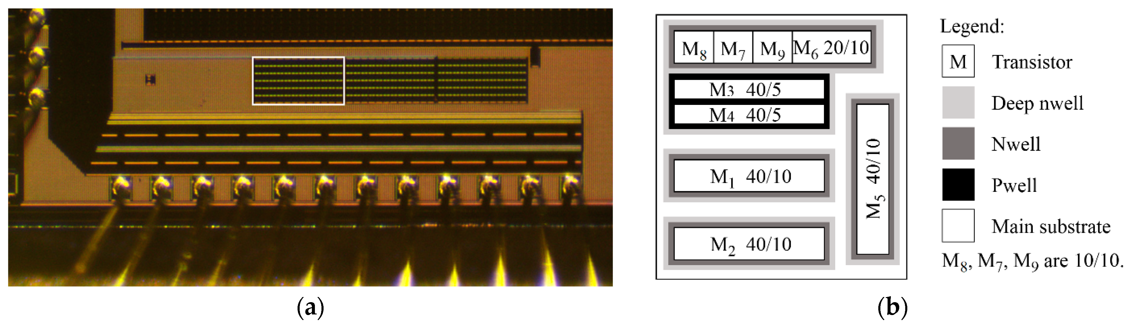
3.1. The Chip and Measurements

The filter was implemented in the integrated circuit shown in Figure 4a. A white rectangle indicates an area of the filter, which is 128 µm by 258 µm, including metal-insulator-metal (MIM) capacitors. MIM capacitors cover the entire filter; hence, no transistors are visible in the micro photo.
The arrangement of transistors inside the filter cell is illustrated in Figure 4b. The filter cell contains transistors M1 to M9; their dimensions, W/L in µm/µm, are as follows: M1 and M2, 40/10; M3 and M4, 40/5; M5, 40/10; M6, 20/10; and M7, M8, and M9, 10/10. Transistors M10 and M11 are outside the cell because they are wide (one hundred parallel-connected 10/10 devices each) to conduct off-chip bias currents. All transistors are thin-oxide low-VT devices with threshold voltages (VT) of 0.34 V and −0.39 V for n and p type devices, respectively. Low threshold voltages are necessary due to the 0.5 V supply voltage. As low-VT transistors have relatively high channel leakage, long 10 µm channels are used, which reduce leakage to much below 0.1 nA at temperatures up to 50 °C.
In the following, measurement results for the filter operating using the supply voltage VDD = 0.5 V, a gate bias voltage VB = 150 mV, and input DC level of 360 mV are reported.
Figure 5 illustrates the Q tuning process, along with an IQ ranging from 40 to 0.1 nA. On successive screens from the analyser, it is seen that Q increases from 6.7 dB (2.16) to 21.4 dB (11.74), and there is no deviation in ω0 (1 kHz). Thus, this observation addresses (7), and confirms that the sensitivity of Q to R1 is much greater than that of ω0 to R1.
The frequency tuning range was also examined. The consecutive screens in Figure 6 present the measured filter amplitude responses, in which ω0 increases from 500 Hz to 2.5 kHz, with IBIAS from 1.4 to 7.7 nA. In this case, the quality factor varies due to changes in transistor conductances: the Q deviation is ±12% or ±2%, assuming a tuning range of 0.5–2.5 kHz or 1–1.5 kHz, respectively. Quality factor deviations can be compensated by appropriate corrections of IQ. For example, ω0 and Q are 1 kHz and 21 dB, respectively, at an IBIAS of 2.9 nA and an IQ of 0.1 nA. If ω0 is set to 1.5 kHz using an IBIAS of 4.5 nA, then IQ must be corrected to 0.3 nA to maintain the quality factor at the same level.
Figure 7a,b show the filter noise density and total-harmonic-distortion (THD) parameter measured at the filter output, respectively. The total noise, referred to the filter input and integrated from 100 Hz to 2 kHz, is 70 µVRMS. The 1% output THD occurs with an input 200 Hz sine wave with an amplitude of 67 mVRMS, which results in a signal-to-noise (S/N) ratio of 59.7 dB.
Measured filter parameters are summarized in Table 1. Power consumption ranges from 2.2 to 52 nW, depending on the Q and ω0 values. The power and noise performance of the filter presented in this work are better compared to other solutions, except that of [23]. In terms of quality factor range, the realization of this work meets the minimum requirements for cochlear applications (a Q range of 2–11). The best Q range, 1.3–39, was reported in [14].
The frequency tuning range of this work’s filter, 0.5–2.5 kHz, cannot be meaningfully compared, because other references report only the frequency range of an entire bank of filters (e.g., 0.1–20 kHz), and not those of individual filters.
The next section discusses the frequency range of a filter bank assuming use of the filter presented in Figure 1a.

3.2. Filter Bank Design Example (Simulations)

A filter bank is a cascade of filters with different nominal cut-off frequencies. To change the nominal cut-off frequency of the filter in Figure 1a, the circuit must be redesigned by appropriately scaling the bias current, capacitance, and transistor dimensions. Taking into account practical design limits, such as a minimum transistor bias current of 0.5 nA (which implies that IBIAS ≥ 1 nA) and the upper capacitance limit of 100 pF, the cut-off frequency can be scaled down to 500 Hz, according to Table 2.
On the other side, the upper range of the cut-off frequency is limited by two factors: a minimum value of filter capacitance allowed due to mismatch, and a maximum value of IBIAS related to a power limit. So, based on the worst power case selected from Table 1 (which is [12]), the practical limit of 20 µW per single filter in a bank can be assumed, which is well above the 52 nW achieved in this work. Nevertheless, scaling up IBIAS involves upscaling the transistors’ widths (according to scaling factor M in Table 2), which results in a larger parasitic capacitance at node A. This parasite limits the cut-off frequency to 8 kHz, which is quite sufficient for speech recognition systems.

4. Discussion

Selecting an appropriate filter structure to build a filter bank is related to the method for tuning the filter quality factor. Depending on the filter structure, the quality factor is adjusted by changing a specific circuit parameter, e.g., the amplifier gain, transconductance, resistance, etc. However, changes in circuit parameters always affect the filter cut-off frequency to a greater or lesser extent. Figure 8 schematically illustrates three different methods of Q tuning: the one proposed in this paper and two others that are applicable to transconductance-C (Gm-C) filter structures. These three methods are briefly discussed and compared.
The filter shown in Figure 8a uses a loop-in voltage attenuator (A) to tune the quality factor [23]. This method is the only one among those illustrated that allows for fully independent control of the quality factor and cut-off frequency. The disadvantage of this scheme is a certain difficulty in implementing the attenuator, which must attenuate only AC signals, not DC signals.
In the classic method illustrated in Figure 8b, the quality factor is tuned independently by means of the additional transconductance G3 [16,17,18,24]. Independent tuning of the cut-off frequency is possible, but G1/G2 and G3/G2 ratios must be kept constant. Therefore, the robustness of this filter to the transconductance mismatch is weaker compared to that of the other solutions.
The technique proposed in this paper (Figure 8c) uses the adjustable output resistance of a transconductance amplifier to tune the filter quality factor. This is a compromised solution, because the quality factor can be controlled independently, while frequency tuning causes some deviations in the Q factor. The robustness of filter characteristics to technological mismatch is at a satisfactory level despite the capacitance disparity (C1 << C2), as previously mentioned. The proposed quality factor tuning technique’s advantages include relatively simple implementation, because it does not require additional amplifiers, transconductors, etc., but only requires simple DC current sources.

5. Conclusions

The filter presented in this paper can be used to implement low-cost filter banks that emulate the characteristics of the cochlea over the speech frequency range. The proposed filter belongs to the class of buffer-based filters [25] characterized by a DC voltage gain close to unity and an insensitivity to mismatch in the filter passband. Therefore, the proposed filter is suitable for both parallel and cascade banks.

Author Contributions

J.J. and W.J. contributed equally in conceptualization, methodology, formal analysis, simulations, writing—original draft preparation, and writing—review and editing. All authors have read and agreed to the published version of the manuscript.

Funding

This research received no external funding.

Data Availability Statement

Data are contained within the article.

Conflicts of Interest

The authors declare no conflicts of interest.

References

  1. Karrenbauer, J.; Klein, S.; Schönewald, S.; Gerlach, L.; Blawat, M.; Benndorf, J.; Blume, H. SmartHeaP—A High-level Programmable, Low Power, and Mixed-Signal Hearing Aid SoC in 22 nm FD-SOI. In Proceedings of the 48th IEEE European Solid State Circuits Conference, ESSCIRC 2022, Milan, Italy, 19–22 September 2022; pp. 265–268. [Google Scholar] [CrossRef]
  2. Raychowdhury, A.; Tokunaga, C.; Beltman, W.; Deisher, M.; Tschanz, J.W.; De, V. A 2.3 nJ/frame voice activity detector-based audio front-end for context-aware system-on-chip applications in 32-nm CMOS. IEEE J. Solid-State Circuits 2013, 48, 1963–1969. [Google Scholar] [CrossRef]
  3. Price, M.; Glass, J.; Chandrakasan, A.P. A 6 mW, 5000-word real-time speech recognizer using WFST models. IEEE J. Solid-State Circuits 2015, 50, 102–112. [Google Scholar] [CrossRef]
  4. Yang, G.; Lyon, R.F.; Drakakis, E.M. A 6 μW per channel analog biomimetic cochlear implant processor filterbank architecture with across channels AGC. IEEE Trans. Biomed. Circuits Syst. 2015, 9, 72–86. [Google Scholar] [CrossRef] [PubMed]
  5. Harczos, T.; Chilian, A.; Husar, P. Making use of auditory models for better mimicking of normal hearing processes with cochlear implants: The SAM coding strategy. IEEE Trans. Biomed. Circuits Syst. 2013, 7, 414–425. [Google Scholar] [CrossRef] [PubMed]
  6. Yip, M.; Jin, R.; Nakajima, H.H.; Stankovic, K.M.; Chandrakasan, A.P. A Fully-Implantable Cochlear Implant SoC With Piezoelectric Middle-Ear Sensor and Arbitrary Waveform Neural Stimulation. IEEE J. Solid-State Circuits 2015, 50, 214–229. [Google Scholar] [CrossRef] [PubMed]
  7. Russo, M.; Stella, M.; Sikora, M.; Pekić, V. Robust Cochlear-Model-Based Speech Recognition. Computers 2019, 8, 5. [Google Scholar] [CrossRef]
  8. Ma, T.; Shen, C.; Wei, Y. Adjustable Filter Bank Design for Hearing Aids System. In Proceedings of the 2019 IEEE International Symposium on Circuits and Systems, ISCAS 2019, Sapporo, Japan, 26–29 May 2019; pp. 1–5. [Google Scholar] [CrossRef]
  9. Wei, Y.; Ma, T.; Ho, B.K.; Lian, Y. The Design of Low-Power 16-Band Nonuniform Filter Bank for Hearing Aids. IEEE Trans. Biomed. Circuits Syst. 2019, 13, 112–123. [Google Scholar] [CrossRef] [PubMed]
  10. Özbek, B.; Külah, H. A 1-V Nanopower Highly Tunable Biquadratic GmC Bandpass Filter for Fully Implantable Cochlear Implants. In Proceedings of the 2021 IEEE Biomedical Circuits and Systems Conference, BioCAS 2021, Berlin, Germany, 6–9 October 2021; pp. 1–5. [Google Scholar] [CrossRef]
  11. Özbek, B.; Külah, H. A 9.03 µW Low Noise Highly Tunable Analog Front-End for Fully Implantable Cochlear Prosthesis. In Proceedings of the 2022 IEEE Biomedical Circuits and Systems Conference, BioCAS 2022, Taipei, Taiwan, 13–15 October 2022; pp. 349–353. [Google Scholar] [CrossRef]
  12. Wang, S.; Koickal, T.J.; Hamilton, A.; Cheung, R.; Smith, L.S. A bio-realistic analog CMOS cochlea filter with high tunability and ultra-steep roll-off. IEEE Trans. Biomed. Circuits Syst. 2015, 9, 297–311. [Google Scholar] [CrossRef] [PubMed]
  13. Sarpeshkar, R.; Salthouse, C.; Sit, J.J.; Baker, M.W.; Zhak, S.M.; Lu, T.T.; Turicchia, L.; Balster, S. An ultra-low-power programmable analog bionic ear processor. IEEE Trans. Biomed. Eng. 2005, 52, 711–727. [Google Scholar] [CrossRef] [PubMed]
  14. Yang, M.; Chien, C.-H.; Delbruck, T.; Liu, S.-C. A 0.5 V 55 μW 64 × 2 Channel Binaural Silicon Cochlea for Event-Driven Stereo-Audio Sensing. IEEE J. Solid-State Circuits 2016, 51, 2554–2569. [Google Scholar] [CrossRef]
  15. Lyon, R.F.; Mead, C. An analog electronic cochlea. IEEE Trans. Acoust. Speech Signal Process 1988, 36, 1119–1134. [Google Scholar] [CrossRef]
  16. Watts, L.; Kerns, D.A.; Lyon, R.F.; Mead, C.A. Improved implementation of the silicon cochlea. IEEE J. Solid-State Circuits 1992, 27, 692–700. [Google Scholar] [CrossRef]
  17. Sarpeshkar, R.; Lyon, R.F.; Mead, C.A. An analog VLSI cochlea with new transconductance amplifiers and nonlinear gain control. In Proceedings of the 1996 IEEE International Symposium on Circuits and Systems, Circuits and Systems Connecting the World, ISCAS 96, Atlanta, GA, USA, 15 May 1996; Volume 3, pp. 292–296. [Google Scholar] [CrossRef]
  18. Liu, S.-C.; van Schaik, A.; Minch, B.A.; Delbruck, T. Asynchronous binaural spatial audition sensor with 2 × 64 × 4 channel output. IEEE Trans. Biomed. Circuits Syst. 2014, 8, 453–464. [Google Scholar] [CrossRef] [PubMed]
  19. Suzuki, Y.; Takeshima, H. Equal-loudness-level contours for pure tones. J. Acoust. Soc. Am. 2004, 116, 918–933. [Google Scholar] [PubMed]
  20. Ruggero, M.A.; Shyamla Narayan, S.; Temchin, A.N.; Recio, A. Mechanical bases of frequency tuning and neural excitation at the base of the cochlea: Comparison of basilar-membrane vibrations and auditory-nerve-fiber responses in chinchilla. Proc. Natl. Acad. Sci. USA 2000, 97, 11744–11750. [Google Scholar] [CrossRef] [PubMed]
  21. Alioto, M. Ultra-Low Power VLSI Circuit Design Demystified and Explained: A Tutorial. IEEE Tran. Circuits Syst. II Reg. Pap. 2012, 59, 3–29. [Google Scholar] [CrossRef]
  22. Enz, C.; Krummenacher, F.; Vittoz, E.A. An analytical MOS transistor model valid in all regions of operation and dedicated to low-voltage and low-current applications. J. Anal. Integr. Circuits Signal Process 1995, 8, 83–114. [Google Scholar] [CrossRef]
  23. Jendernalik, W.; Jakusz, J.; Blakiewicz, G. Low-Voltage Low-Power Filters with Independent ω0 and Q Tuning for Electronic Cochlea Applications. Electronics 2022, 11, 534. [Google Scholar] [CrossRef]
  24. Grech, I.; Micallef, J.; Azzopardi, G.; Debono, C.J. A 0.9 V wide-input-range bulk-input CMOS OTA for GM-C filters. In Proceedings of the 10th IEEE International Conference on Electronics, Circuits and Systems, ICECS 2003, Sharjah, United Arab Emirates, 14–17 December 2003; Volume 2, pp. 818–821. [Google Scholar] [CrossRef]
  25. Jendernalik, W.; Jakusz, J.; Blakiewicz, G. Ladder-Based Synthesis and Design of Low-Frequency Buffer-Based CMOS Filters. Electronics 2021, 10, 2931. [Google Scholar] [CrossRef]
Figure 1. Proposed filter: (a) detailed schematic; and (b) equivalent small-signal, Gm-C network.
Electronics 13 00399 g001
Figure 2. Monte Carlo simulation results (Cadence Spectre) of the 1 kHz filter in Figure 1a.
Electronics 13 00399 g002
Figure 3. Noise schematics for: (a) the whole filter; (b) the amplifier G1; and (c) the amplifier G2.
Electronics 13 00399 g003
Figure 4. Fabricated filter: (a) micro photo; and (b) simplified view of a filter cell. Transistor dimensions, W/L, are in µm/µm.
Electronics 13 00399 g004
Figure 5. Tuning of Q measured at ω0 of 1 kHz. IQ is 40, 30, 20, 10, 1, and 0.1 nA. IBIAS is 2.9 nA.
Electronics 13 00399 g005
Figure 6. Tuning of ω0 at Q of 21dB. IBIAS is 1.4, 2.9, 4.5, 6, and 7.7 nA. IQ is 0.1 nA.
Electronics 13 00399 g006
Figure 7. Measured (a) output noise of the 1 kHz filter with Q = 2; and (b) output THD vs. input amplitude.
Electronics 13 00399 g007
Figure 8. Methods used to tune a quality factor using: (a) a voltage attenuator; (b) an additional transconductor; and (c) a transconductor’s output resistance.
Electronics 13 00399 g008
Table 1. Performance comparison of low-frequency filters with tunable Q.
ParameterThis Work[23]
Simulated
[18][12][13][14]
Process0.18 µm0.18 µm0.35 µm0.35 µm1.5 µm0.18 µm
Supply0.5 V0.5 V3.3 V3.3 V2.8 V0.5 V
Power2.2–52 nW8.25–10.75 nWNA13–20 µW 10.1–5.4 µW0.1–100 nW 2
ω00.5–2.5 kHz1.28 kHz0.1–20 kHz
bank
0.31–8 kHz
bank
0.2–6 kHz
bank
0.08–20 kHz
bank
Q2–112–40NA2–191–101.3–39
S/N59 dB68 dB36–52 3 dB17–32 dB57 dB40–55 dB
1 Estimated. 2 Estimated assuming no PGA. 3 With PGA.
Table 2. Scaling a filter bank—simulations 1.
ω0 (kHz)C2 (pF)IBIAS (nA)M 2IQ (nA) P (nW)
Q = 11.22
(21 dB)
Q = 5.01
(14 dB)
Q = 11.22
(21 dB)
Q = 5.01
(14 dB)
0.5601.4210.0251.542.1553.67
1602.9310.1363.14.5317.495
2306.0120.4536.29.46815.215
4159.1220.1985.8313.87819.51
87.59.420.0555.9514.15520.05
1 Process: X-FAB 180-nm (xh018). Transistors: thin oxide 1.8 V, low VT. 2 Transistor multiplication factor (the number of parallel connected transistors).
Disclaimer/Publisher’s Note: The statements, opinions and data contained in all publications are solely those of the individual author(s) and contributor(s) and not of MDPI and/or the editor(s). MDPI and/or the editor(s) disclaim responsibility for any injury to people or property resulting from any ideas, methods, instructions or products referred to in the content.

