Article

A Novel Impedance Matching of Class DE Inverter for High Efficiency, Wide Impedance WPT System

1
School of Aerospace Science and Technology, Xidian University, Xi’an 710126, China
2
Shanghai Institute of Satellite Engineering, Shanghai 201109, China
*
Author to whom correspondence should be addressed.
Electronics 2024, 13(5), 959; https://doi.org/10.3390/electronics13050959
Submission received: 14 January 2024 / Revised: 22 February 2024 / Accepted: 26 February 2024 / Published: 1 March 2024

Abstract

:
In high-frequency wireless power transfer (WPT) applications, Class D, E, and F inverters are most widely used. Class DE inverters combine the respective advantages of Class D and Class E inverters. However, the Class DE inverter is sensitive to changes in impedance, which can easily lead to the loss of soft switching characteristics, thereby reducing efficiency. In this paper, an impedance-matching compensation design method is proposed to expand the high-efficiency region of the Class DE inverter by matching impedance and parameters. The effect of the method on the zero-voltage switching (ZVS) characteristic of Class DE inverters is analyzed in detail. The proposed WPT system maintains a constant voltage and zero phase angle by employing PS/PS compensation topology. Theoretical analysis shows that the impedance can be compressed for the design of resonant network impedance, and the method can expand the high-efficiency region with a reasonable choice of parameters to match the phase. Finally, a 500 kHz, 1 kW WPT prototype was constructed with a coupling factor of 0.25–0.4 and a load range of 30–80 Ω. The inverter’s efficiency exceeds 95%, with optimal efficiency reaching 97.3%. The system efficiency is greater than 87%.

1. Introduction

Magnetic resonance-based wireless power transfer (WPT) technology is being continuously developed, and it is widely used in electronics, electric vehicles, and other consumer fields. It also plays a vital role in some special charging applications [1,2,3,4,5]. In terms of charging for light rail trains, a coupling mechanism is installed on the rail and the train chassis to obtain stable power transfer for train operation [6]. In the field of implantable medical devices, WPT technology makes it more convenient to charge implantable devices, such as heart pumps, without the need for surgery, thereby reducing the difficulty of treatment [7,8,9]. Some scholars have designed WPT systems for underwater equipment, which effectively improves their endurance [10].
In order to optimize and improve the efficiency of the WPT system, researchers have conducted in-depth studies on inverters, coupling coil design, compensation networks, and control methods. References [11,12,13] utilized control strategies such as phase shift, maximum efficiency point tracking (MEPT), and pulse density modulated (PDM) approaches to improve system efficiency and achieve a stable output. This type of control method is usually based on a full-bridge inverter to produce a stable output, and its operating frequency for electric vehicles is typically fixed at 85 kHz. In high-frequency WPT systems, reducing the parasitic resistance of coupling coils can improve transmission efficiency. In publications [14,15], the authors studied the impact of coil parasitic resistance and skin effect on system power and efficiency. They proposed a compromise solution to lower coil resistance and skin effect, thereby improving transmission efficiency. By designing the coil compensation method, reactive power compensation can be achieved, thereby maximizing the transmission power. Yeong H. Sohn et al. conducted a comprehensive comparison of eight basic compensations, including SS, SP, etc. They found that SS and SP compensations exhibited superior properties in terms of maximum efficiency, maximum power transfer, load decoupling, and coupling coefficient decoupling. However, the primary side input impedance varied dramatically, and there were disadvantages, such as short circuits [16,17,18]. On the basis of single-element compensation, researchers have proposed many novel compensations. LCC/S and LC/S compensation structures have been proposed, which also exhibit constant current and constant voltage characteristics, as well as coupling independence and better ZVS or ZCS characteristics [19,20]. Si Li et al. successively proposed a tuning method for the LCC/LCC compensated topology in the application of wireless charging for electric vehicles. This method can easily achieve characteristics such as ZVS and constant voltage [21,22]. The research above focussed more on compensation methods for decoupling coupling coils. In the design of a high-frequency WPT system, more Class E and Class D inverters are used to improve transmission efficiency. However, these types of inverters are sensitive to variations in loads and coil position. The impedance matching method in RF is more suitable for high-frequency situations when using Class E and Class D inverters. When considering the coupling dependence during impedance matching, it is important to accurately analyze the impedance of the inverter.
An increase in operating frequency will lead to higher losses in the switching transistor at the transmitter side when designing high-frequency, high-power WPT systems. In order to solve this issue, Class E inverters can improve the transmission efficiency of the system by achieving ZVS and ZVDS characteristics with only one transistor [23,24,25]. However, Class E inverters are sensitive to variations in loads and component parameters, which often leads to impedance mismatch and decreased efficiency. Design methods for impedance extension have been introduced in order to overcome this drawback [26,27]. It improves the robustness of the system; however, it does not address the high voltage and current stresses. Therefore, new and improved single-transistor inverters of Class F and Class Φ have been developed from Class E, utilizing harmonics for waveform peak shaping, which can effectively reduce the occurrence of high stress [28,29,30]. However, it still fails to meet the requirements of high power due to the use of one single transistor. Class D inverters have low voltage stress, making them widely used in the field of high-frequency, high-power WPT systems [31]. However, the nonlinearity of the MOSFET’s parasitic capacitance makes it challenging to accurately implement ZVS characteristics. Hamed T. addressed this problem by constructing an LC auxiliary network at the midpoint of the H-bridge. It achieves the ZVS characteristics over a wider range of Smith impedance circles [32,33,34,35]. The introduced LC auxiliary network is sensitive to the voltage stress on the MOSFET because it is positioned at the midpoint of the bridge. Furthermore, redundant auxiliary networks are not appropriate for high-power applications. Based on a 6.78 MHz Class E inverter, publications [36,37] proposed methods for optimizing a two-port impedance matching network and impedance compression network design. These methods have the advantage of enhancing the robustness of the coil in misalignment. Paper [38] utilized an adaptive impedance matching network based on Class E to address changes in the load and coil position. However, this method requires array capacitance and search algorithms, making it more complex to implement. There are various design methods for parameters and impedance in WPT systems. Intelligent algorithms and deep learning can also be used to optimize these parameters and impedance [39,40]. Combining the advantages of Class D and Class E inverters, Hirotaka K. et al. first proposed a Class DE-tuned power amplifier, which achieved a power transmission efficiency of 96% at 1 MHz [41]. Researchers have provided accurate time domain analysis waveforms and a parameter design approach for the half-bridge Class DE [42,43]. On this basis, the steady-state time-domain analysis of the full-bridge Class DE was proposed [44]. However, few people have investigated the application of Class DE inverters in wireless power transfer, although some researchers have described the use of half-bridge Class DE inverters in WPT systems at low power, which enables low-power and high-efficiency power transfer at fixed loads [45]. Previous studies [46] have utilized Class DE inverters to achieve applications of wireless power transfer such as 100 W LED lighting. The aforementioned studies focus on the application and tuning of Class DE inverters in wireless power transfer in engineering. They did not discuss or study changes in load and coil position offsets like Class E inverters, nor did they propose corresponding impedance-adaptive solutions. Inheriting the load-sensitive characteristics of Class E inverters, Class DE inverters exhibit high sensitivity to components and loads. We can use impedance matching network optimization to achieve ZVS over a wide range of loads and enhance the impedance robustness of Class DE inverters in WPT systems. Currently, few studies have been conducted on the ZVS characteristics of Class DE inverters in WPT regarding impedance changes. Based on this issue, this article focuses on a design approach using impedance analysis that is suitable for high-frequency Class DE inverters in WPT systems.
Therefore, this paper will investigate how the ZVS characteristics of Class DE inverters are affected by changes in the impedance during impedance matching of the WPT system. We introduce a coil impedance matching compensation method tailored for Class DE inverters and suggest a π 1 a resonant network [47] and a parameter design approach suitable for Class DE inverters. This design approach achieves the ZVS characteristics in a wide impedance range of Class DE inverters, while maintaining the high efficiency of the inverter and system. This article is structured as follows: Section 2 presents the coil PS/PS impedance matching compensation structure, along with an analysis of how variations in load magnitude and coil position affect the input impedance. Section 3 analyses the effect of impedance on ZVS. The Class DE inverter for wide impedance ZVS is designed and optimized. Building the system based on the design for experiments is the focus of Section 4. We will discuss the experimental and simulation results and verify the feasibility of the method. The conclusion is finally presented in Section 5.

2. Characterization of Coupling Coils for PS/PS Impedance Matching Compensation

As shown in Figure 1, the Class DE wireless power transfer system mainly consists of the Class DE inverter, symmetrical PS/PS capacitor compensation network, coupling coils, and rectifier. The system is designed using a component impedance matching method. On both the primary and secondary sides of the coupling coil, resonance compensation is achieved through the use of symmetrical parallel-series capacitors. When the coupling coil is in its ideal position, the equivalent input impedance ZR of the rectifier is directly reflected onto the inverter’s load. The impedance seen from the transmit port is Zin, therefore the equivalent load of the inverter is ZR.
Z i n = Z R ,
The Class DE inverter utilizes a composite resonant network, which includes a π1a impedance matching network, with shunt capacitance CP = C3 + C2. The load of the receiving coil mentioned above is equivalent to the input impedance of the full-bridge rectifier circuit, denoted as ZR [48]:
Z R = 8 π 2 R L .

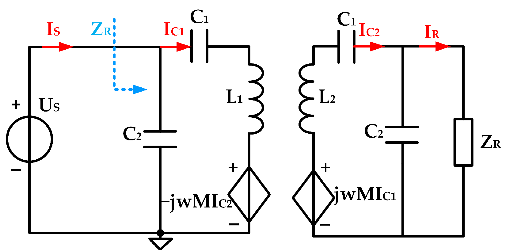
2.1. Coils PS/PS Impedance Matching Compensation

The decoupled equivalent circuit model is displayed in Figure 2. We disregard the parasitic characteristics of the transmitter and receiver coils’ inherent capacitance and inductance and treat them as a two-port network. To finish the impedance matching, we used symmetrical PS/PS capacitors, C1 and C2. By adopting the impedance matching approach, we can more effectively determine the matching parameters L1 and L2 of the coupling coils to achieve reactive power compensation at various locations. Based on the KVL and KCL equations, we can describe the circuit model shown in Figure 2. The currents and voltages in bold in the equation below are in phase form.
( I S I C 1 ) 1 j ω C 2 j I C 1 ( ω L 1 1 ω C 1 ) + j ω M I C 2 = 0 j ω M I C 1 + I C 2 j ω L 2 1 ω C 1 + Z R 1 + j ω Z R C 2 = 0 U S + ( I S I C 1 ) 1 j ω C 2 = 0 I R Z R I C 2 I R 1 j ω C 2 = 0 .
By introducing intermediate impedance variables Z1 and Z2, the analysis can be further simplified to assist in solving Equation (3):
Z 1 = ω L 1 1 ω C 1 Z 2 = j ω L 2 1 ω C 1 + Z R 1 + j ω Z R C 2 .
The coupling factor k of the coils can be expressed as the relationship between the mutual inductance M and L1, L2.
M = k L 1 L 2 ,
Combining Equations (2)–(5), they can be solved to obtain the receiving coil input impedance Zin:
Z i n = U S I S = j ω C 2 + Z 2 Z 1 Z 2 ω k 2 L 1 L 2 .
To achieve port impedance matching, the load can be directly reflected back to the transmitter, satisfying the scattering S-parameter matching condition in the RF field. As shown in Equation (7), Zin is based on the values of the real and imaginary parts. We are able to determine the required matching capacitors, C1 and C2:
Z i n = R e Z i n + j I m Z i n R e Z i n = Z R I m Z i n = 0 .
According to the impedance expressions (6) and (7) for the real and imaginary parts, we can determine the trends of Re (Zin) and Im (Zin) of the equivalent load Zin of the Class DE inverter under variations in the load and coupling coefficient. Figure 3a,b shows that the load ZR = 50 Ω. There is a decrease in real impedance Re (Zin) to less than 50 when the coupling coefficient k is varied between 0.2 and 0.4. Pulling the coils farther away results in a decrease in k , while Im (Zin) > 0 indicates the introduction of inductive variations. Conversely, pulling the coils closer raises k , and Im (Zin) < 0 indicates the introduction of capacitive changes. Therefore, with the PS/PS impedance matching compensation method, the coupling coil offset will cause changes in both the real and imaginary parts. Meanwhile, the coil offset will only result in a smaller real part than ZR. The imaginary part is negatively correlated with the change in the coupling coefficient. When k = 0.3 is fixed, the load ZR varies from 30 Ω to 80 Ω. In Figure 3a, it can be seen that Re (Zin) follows the load, presenting a single increasing linear change with Im (Zin) = 0. All these impedance changes will directly affect the equivalent load of the Class DE inverter.

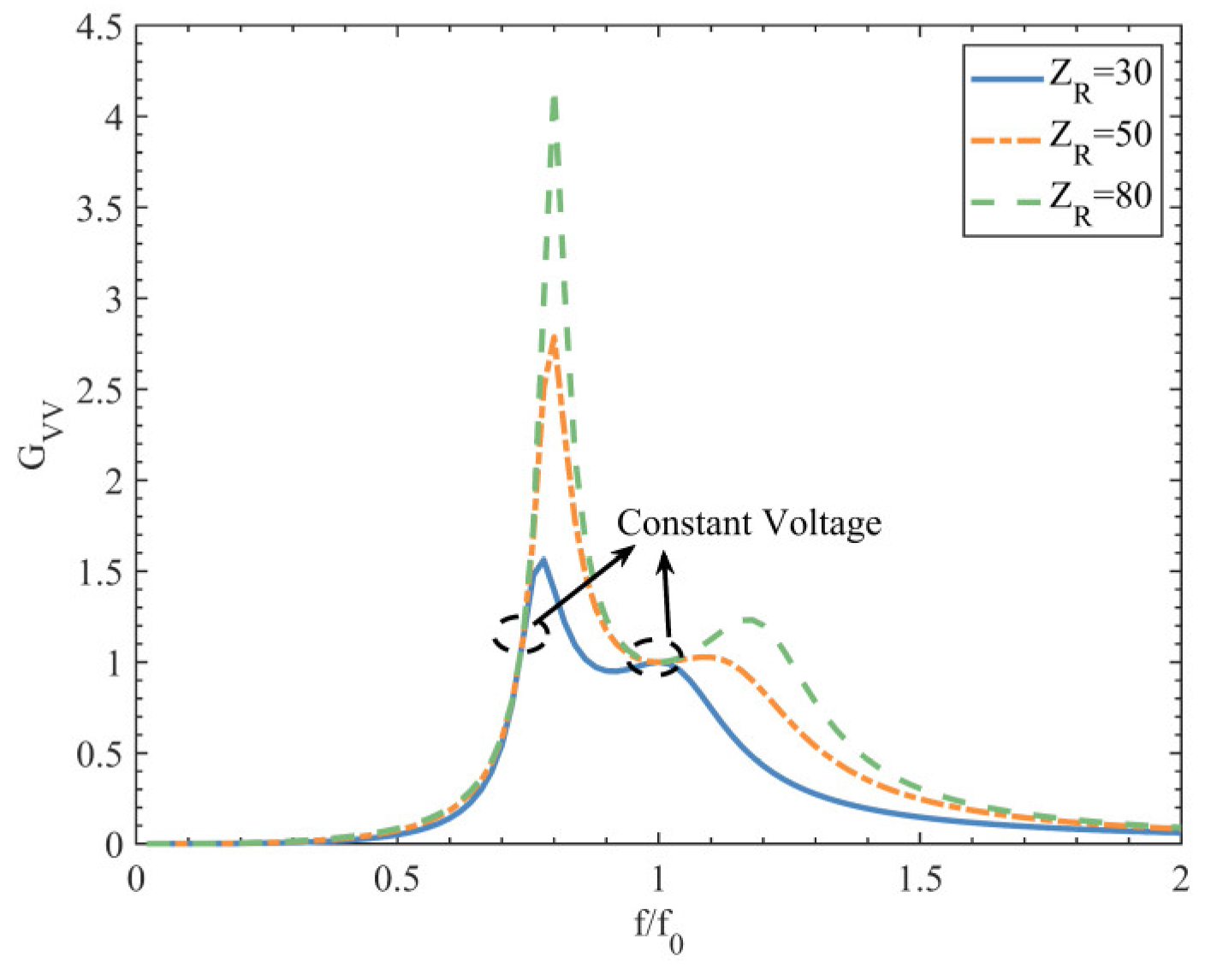
2.2. Voltage Gain and Constant Voltage Characteristics

In contrast to the conventional compensation topology, the coupling coils are compensated by PS/PS impedance matching, which also exhibits constant voltage characteristics in terms of voltage gain and other factors. Based on the system of Equations (2)–(5), we can derive the expression for the magnitude of voltage gain, as shown in Equation (8):
G V = U R U S = Z R C 2 k L 1 L 2 Z R + 1 j ω C 2 Z 1 Z 2 + k ω 2 L 1 L 2 .
Based on the voltage gain expression, a gain plot can be obtained. In Figure 4, the horizontal axis of the graph represents the normalized frequency, while the vertical axis represents the voltage gain. We can see that this impedance-matching compensation method has two constant voltage output points.
To fit the coupling coils to compensate the design and load output characteristics of the actual Class DE inverter, it is essential to achieve zero phase angle characteristics and constant voltage features. As a result, we need to ensure that the constant voltage point falls at the f/f0 = 1.

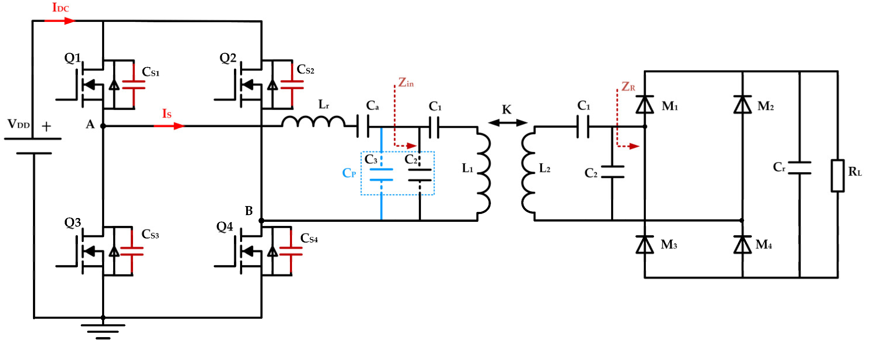
3. Theoretical Analysis and Design of Class DE Inverters

3.1. Theoretical Description of Class DE Inverter

In Figure 1, a Class DE inverter is used as the transmitter-side power DC-AC converter. Based on the conventional full-bridge Class D inverter, four identical capacitors CS1CS4 are used in parallel with the MOSFETs. Table 1 displays the switching modes in the range (0, 2π) for one cycle following the stabilized operation of the Class DE inverter, where D represents the duty cycle of the PWM signal that controls the MOSFETs. During mode ①, Q1 and Q2 are turned on, and the current is(θ) flows positively (setting the flow from point A to point B as positive). During mode ②, all MOSFETs are off, so the resonant cavity must be designed to be weakly inductive. Consequently, the current is(θ) cannot be mutated. It will continue to flow in the positive direction and charge the capacitors CS2 and CS3. Modes ③ and ④ will repeat the process of the first half cycle, so they will not be further elaborated. A sine wave can be used to express the current is(θ), assuming that it is in a steady-state condition. Where Im is the current amplitude and the phase angle θ = ωt, setting the initial phase induced by the resonant network to be φ:
i s θ = I m s i n θ + φ .
We can obtain the expression for the input voltage UAB at port AB of the resonant network by following the description of the four operating modes, which are based on Kirchhoff’s law and capacitor charging and discharging analysis in the time domain [42]. As demonstrated by Equation (10), where the operating frequency of the system is set as f0, and the angular frequency ω = 2πf0:
U A B = V D D 2 I m ω C S c o s θ + φ c o s 2 π D + φ V D D V D D       2 I m ω C S c o s θ + φ + c o s 2 π D + φ + V D D         .
The inverter resonant network allows only the fundamental wave component of UAB to transfer power through the coupling coil. Since Lr and Cr resonate in series at operating frequency f0, as shown in Figure 5b, theoretically, Xr = 0. The Lf represents the phase-shifted inductance of the capacitor CS for charging and discharging. Therefore, according to the Fourier series decomposition, we can decompose UAB into the phase-shifted inductance component and the load RS component. The load voltage URs can be expressed as Equation (11).
U R s = i s θ R S = U m s i n θ + φ .
According to Equation (10), we use Fourier series to decompose UAB, and the amplitude Um on the equivalent load RS can be easily obtained.
U m = 1 π 0 2 π U A B s i n θ + φ d θ = 4 s i n π D + φ s i n ( π D ) π V D D ,
The DC input current IDC of the inverter is an average of the total current of the four modes. In modes ② and ③, the bus does not supply energy; instead, the capacitor CS undergoes charging and discharging cycles. Thus, the total current ia is equal to the sum of the currents iQ1(θ) and iQ4(θ) flowing on Q1 and Q4 in mode ① and mode ④. Thus, the DC current can be expressed as the average amount of current ia:
I D C = 1 2 π 0 2 π i a d θ = 2 s i n π D + φ s i n ( π D ) π I m .
In the ideal case, the output power P o u t of the Class DE inverter should, theoretically, be equal to the input power Pin. In the design, we can determine the relationship between the input and output power and RS according to Equation (14):
P i n = P o u t = U m 2 2 R S = I m 2 R S 2 = V D D I D D .
Combining Equations (12) and (14), the solution for the input voltage of the Class DE can be found:
V D D = R S π 2 8 s i n 2 π D + φ s i n 2 π D P o u t .

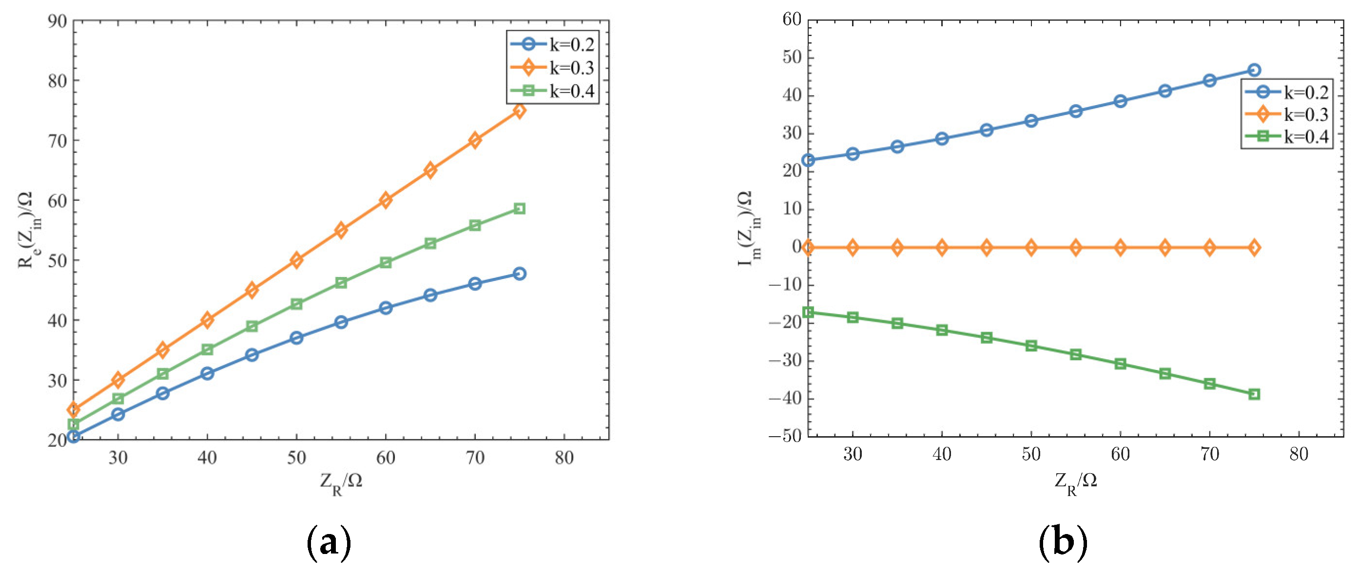
3.2. Analysis of Wide Load ZVS Conditions

After the MOSFET is turned off, three corresponding states exist for the capacitor charging and discharging process due to the inertial current is(θ) caused by inductive reactance. In the initial condition, the MOSFET is unable to attain the ZVS characteristic since is(θ) is unable to completely extract the charge in the capacitor. At the moment the MOSFET is turned on, the charge will be instantaneously drained through the on-resistance. This results in the MOSFET current overshoot, as shown in Figure 6. It can be stated in terms of the voltage of the MOSFET, VS4(2π):
V S 4 2 π > 0   Non   ZVS.
The second state occurs when is(θ) crosses the zero point just as the charge in CSi is drawn out and the voltage across the capacitor becomes zero. As a result, the ZVS characteristic is satisfied and also has the zero derivative ZVDS turn-on for Class E inverters, and optimal operation for Class DE. The voltage on Q4 can be similarly represented in the second half cycle:
V S 4 2 π = 0 Z V S d V S 4 θ d θ = 0   Z V D S .
The third state occurs when is(θ) can fully discharge the charge in the capacitor Csi. The current is(θ) keeps flowing in the original direction, and it will charge the capacitor in the opposite direction. When VS4(θ) ≈ −0.7 V, the capacitor voltage will be clamped by the body diode. The ZVS characteristics of the inverter are displayed in the third plot in Figure 6. The inverter can be operated in a suboptimal state. Thus, the ZVS necessary condition at θ = 2π can be expressed as Equation (18):
V S 4 2 π 0 Z V S d V S 4 θ d θ < 0   N o n Z V D S .
Achieving ZVS across a wide range of load conditions requires finding a balance between the charging and discharging states of the capacitor. For state I, the capacitor can not be fully discharged, and the loss is larger. State II allows the inverter to work optimally; however, it has to finish charging and discharging the capacitor when the current crosses zero. This approach has a high sensitivity to components, making it the best option for state III to obtain robust impedance characteristics. We select an appropriate initial phase angle φ to achieve high efficiency with minimal loss and impedance perturbation capability. The shunt capacitor CSi will significantly reduce the turn-off loss.
According to the above description, combining Equations (9), (10), and (18), we can derive the sufficient condition of ZVS, which is met by the condition of state III:
V D D = I m c o s φ + c o s 2 π D + φ w C s .
The capacitance in the above equation meets the requirement of the sum of the parallel capacitance CSi in the same bridge, i.e.,
C S = C S 1 + C S 3 = C S 2 + C S 4 .
Combining Equations (13) and (19), we can determine the magnitude of the shunt capacitance CS:
C S = 2 s i n 2 π D + φ s i n 2 π D R S π ω .

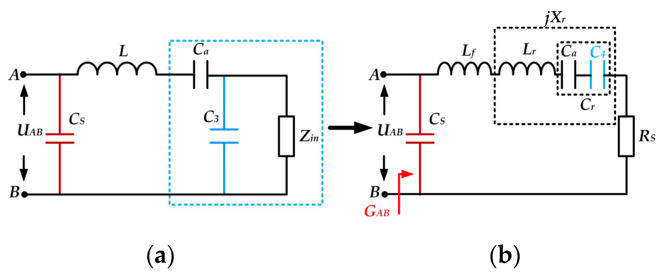
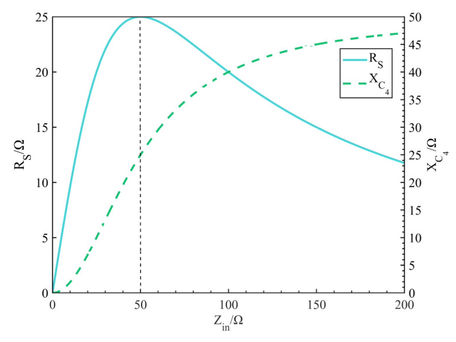
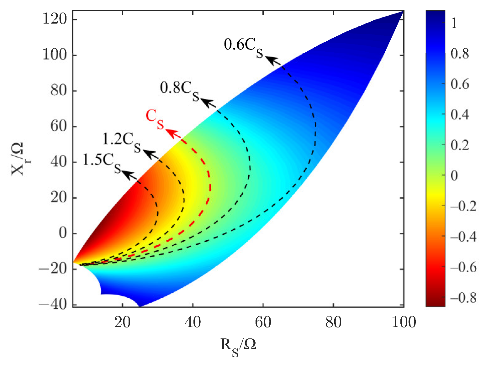
3.3. Wide Load ZVS Matched Resonant Network Design

The idea of this system design is to achieve an impedance-matching design from RS to Zin by using ZR as the impedance-matching node. An π1a impedance matching network is introduced from Figure 5b to Figure 5a. The total impedance of the parallel capacitor C3 and impedance Zin in Figure 5a needs to exactly match the total impedance value of the series capacitor C4 and load RS in Figure 5b. In Figure 5, the reactance factor q of the Zin-C3 and RS-C4 equivalent two-port can be expressed by Equation (22):
q = Z i n X C 3 = X C 4 R S .
From the property of equal impedance of Zin-C3 and RS-C4, we can determine the value of RS:
R S = Z i n 1 + q 2 .
From Equations (22) and (23), the capacitive resistance XC4 of C4 can be obtained here:
X C 4 = Z i n q 1 + q 2 .
The total impedance Z1 of the parallel Zin-C3 can be expressed as follows:
Z 1 = 1 / ω C 3 1 / ω C 3 Z i n + ω C 3 Z i n + j Z i n 1 / ω C 3 Z i n + ω C 3 Z i n .
In Equation (25), a relationship is defined by the function 1/x + x > 2. This indicates the presence of maximum points in both the real and imaginary parts of the impedance Z1.
In Figure 7 the reactance factor q = 1. When the equivalent load Zin is varied, the load RS will be compressed below the maximum value, while the imaginary part of the capacitive reactance XC4 can be compressed below the capacitive reactance XC3. Consequently, we can accomplish simple impedance compression using this π1a Impedance matching network, appropriately extending the range of ZVS for the load.
In Figure 5b, the admittance seen from port AB is denoted as YAB. We can think of the resonant network as capacitor CS in parallel with the back-end series resonant circuit. In Figure 5b, jXr represents the total impedance value of inductor Lr and capacitor Cr, where Cr is composed of series capacitors Ca and C4. Hence, we can determine the conductance YAB:
Y A B = G + j B G = R S R S 2 + X S 2 B = ω C S X S R S 2 + X S 2 X S = ω L f + X r .
The initial phase and amplitude of the current is(θ) are mainly caused by the conductance YAB. We can derive the relationship equation between the initial phase φ and the impedance:
φ = π + t a n 1 B G .
Combining Equations (26) and (27), we can solve the relational function for Lf and φ from the impedance perspective and derive Lf according to Equation (28):
ω C S ( ω L f ) 2 ω L f = t a n φ R S ω C S R S 2 .
In the inverter, we have utilized the circuit topology of LC series resonance, allowing us to determine L from the quality factor Q:
L = Q R S ω .
Based on Equations (28) and (29), we have solved for Lr :
L r = L L f .
Since Lr and Cr resonate at the operating frequency f0, the value of Cr can be obtained:
C r = 1 ω 2 L r .
In the impedance transformation compression network, setting the reactive power factor q to 1 allows us to obtain the values of capacitors C3 and C4 based on Equation (22). As shown in Figure 5b, the capacitor Cr is composed of Ca and C4 in series, so that the value of Ca can be obtained:
C a = 1 ω 2 C r 1 ω 2 C 4 .

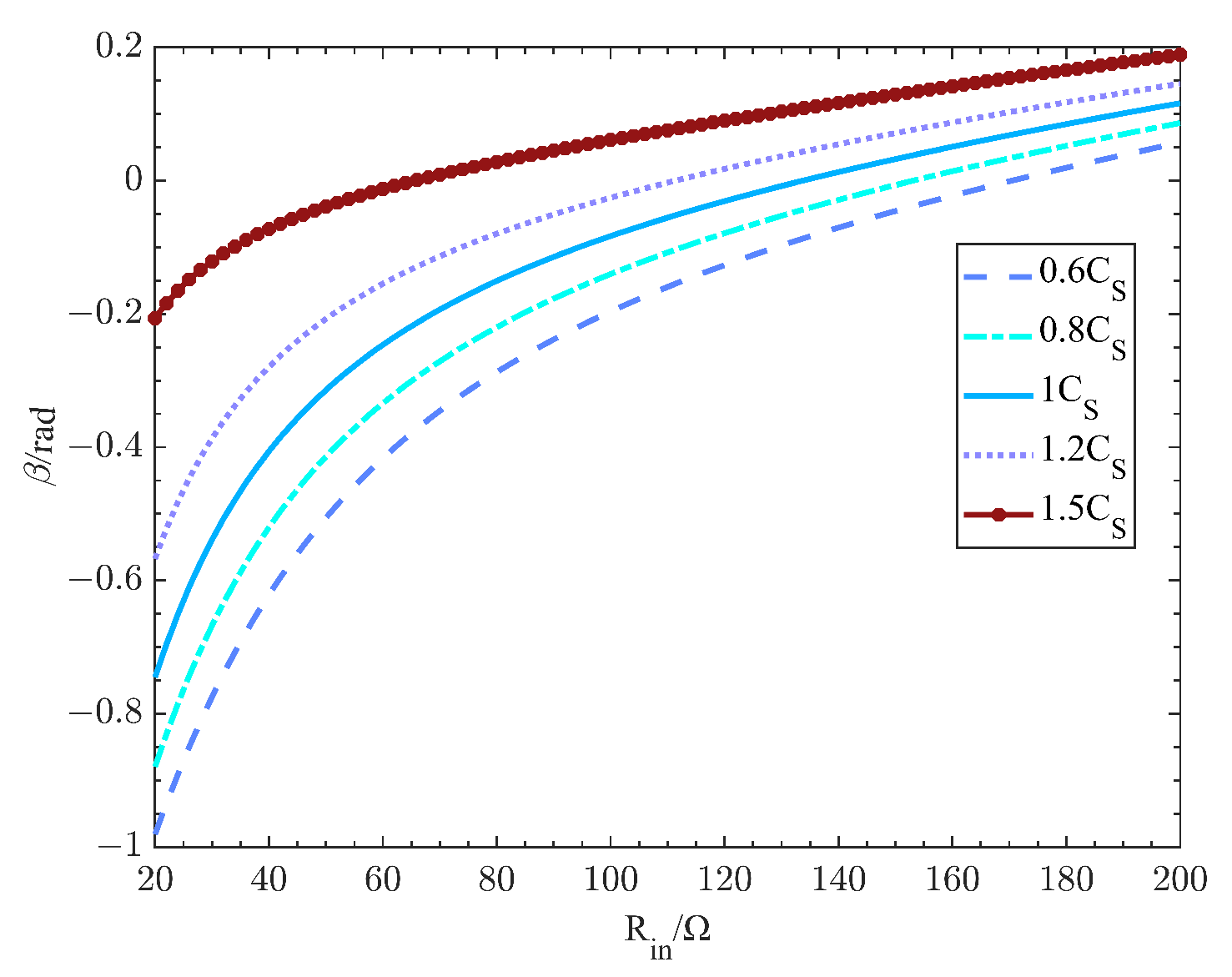
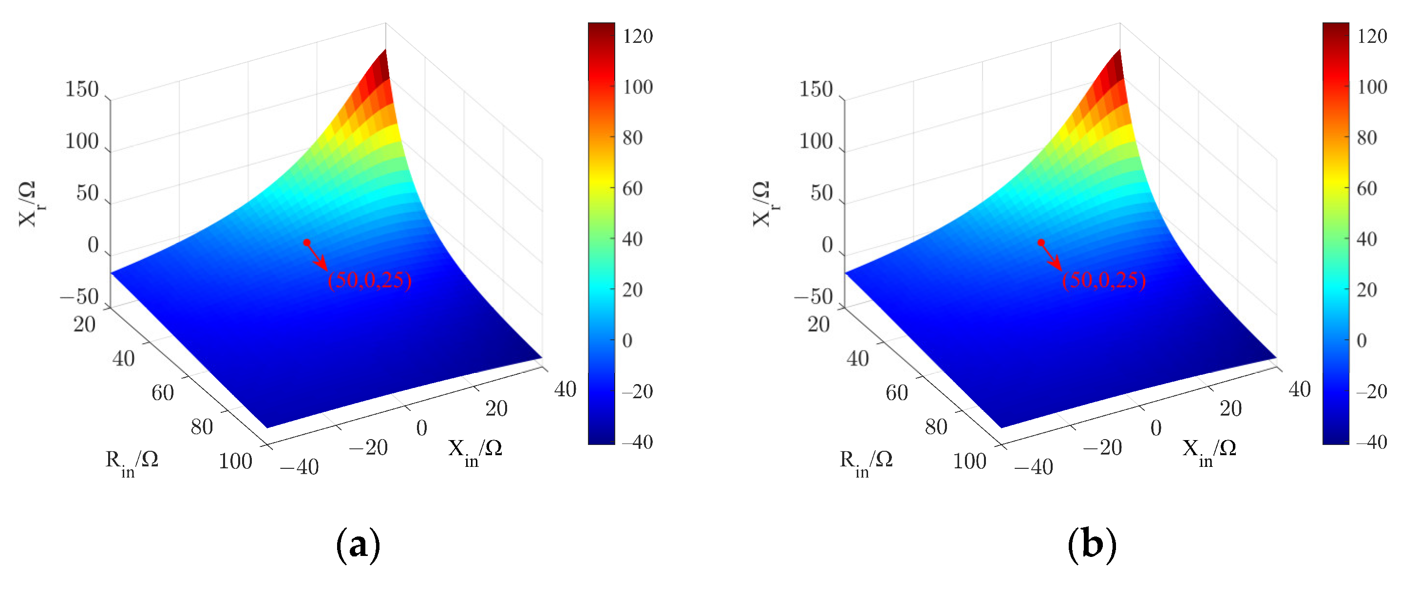
3.4. Analysis of the Effect of Parameter Variations on the Wide Load ZVS

The design methodology for all parameters has been provided in the previous sections. However, further investigation is required to explore the impact of component parameter variations and load variations on the ZVS of the Class DE inverter. To maximize the wide load ZVS characteristics of Class DE inverters with minimal losses. It is necessary to explore the effect of impedance on the initial phase angle φ. In Figure 5b, the impedances jXr and RS actually change with the impedance Zin. Since wireless power transfer is influenced by the coupling coefficient k and the equivalent load ZR, there are two situations for the variation of Zin.
The first situation occurs when the coils are in an optimal state. In this case, there is only a change in the load Rin. According to Figure 3, it is known that the equivalent impedance Zin of the Class DE inverter will not have an imaginary part; only the real part of the impedance changes. According to Equation (25) and Figure 7, it can be observed that RS < 0.5Zin holds constantly. According to Figure 5b and Equation (25), the variation of impedance X r can be expressed as:
X r = ω L r 1 ω C a Z i n 1 / ω C 3 Z i n + ω C 3 Z i n .
The second situation is when there is an offset in the coupling coils. Figure 3b shows that using this compensation design method introduces an imaginary part, while the real part changes less than Zin. Thus, the impedance Zin reflected to the inverter will have both real and imaginary parts:
Z i n = R i n + j X i n .
Due to the presence of the imaginary part, the π1a impedance matching network will not exhibit typical impedance compression characteristics. It has a direct effect on the equivalent impedances RS and Xr in Figure 5b. A complex impedance matching equation can be obtained from Equations (25) and (34):
R S = 1 X C 3 X i n R i n + X C 3 X i n R i n 1 X C 3 X i n 2 + X C 3 R i n 2 X r = ω L r 1 ω C a + 1 X C 3 X i n X i n X C 3 R i n 2 1 X C 3 X i n 2 + X C 3 R i n 2 .
It has been clearly analyzed earlier that the ZVS necessary condition for wide loads needs to be satisfied in Equation (18). From the impedance design perspective, the wide load necessary condition is to ensure that the input current of the resonant network input current lags behind the voltage. Thus, according to Equations (27) and (28), we can obtain the optimality condition for the existence of a wide load ZVS, which is required to keep the conductance angle β at the AB port of the resonant network less than or equal to 0, i.e.,
β = t a n 1 B G 0 .
We can directly determine whether the resonant network is inductive or not based on the admittance angle β. Figure 8 illustrates the effect of shunt capacitance CS with different multiples of α on the admittance angle β at the optimum distance of the coils. It can be seen that a larger load ZR leads to an increase in β, and there exists a value such that β = 0. This is the critical value for the realization of ZVS. The range of load ZR for β < 0 can be expanded when the design value αCS is less than or equal to the theoretical value CS. There will be a decrease in the load ZR range for β < 0 When αCS < CS. Therefore, to achieve wide load ZVS, α < 1 can be taken moderately in designing the parameters. In this paper, the α coefficient is set at 0.85, which expands the ZVS region. However, an excessively small α can also lead to increased reactive power and longer body diode recovery time.
Figure 9 illustrates the variations in RS and Xr in the resonant network of the inverter, which result from changes in the imaginary and real parts caused by coil offsets. In Figure 9a, according to the resonance network in Figure 5, we designed the theoretical value Xr = 0. However, the variation in the coil position will lead to a change in the imaginary part. In Figure 9a, when Xin > 0, this results in Xr > 0, leading to a smaller conductance angle β. At this point, ZVS state III is still satisfied and can be said to be over ZVS. Conversely, working in state II, ZVS is completely lost. In Figure 9b, the imaginary part X i n is excessively large, leading to a significant variation of R S , indicating the failure of the π1a impedance matching network.
Figure 10 illustrates the impact of variations in RS, Xr, and αCS on the ZVS region. Where the color change represents the magnitude of β at the theoretical value of CS, the dashed region indicates β < 0, which we consider achievable for ZVS. We can see that α < 1 for coils offset also widens the ZVS region, thus canceling out the effect of the imaginary part introduced by coils offset on the Class DE inverter.
In summary, lowering the value of CS to sacrifice a small portion of reactive power can widen the ZVS region of the Class DE inverter and improve the overall system efficiency, regardless of whether the coil is offset or the load is altered. The combination of impedance transformations in compression networks, along with selected values of CS can enhance the impedance robustness characteristics of wireless power transfer systems without escalating the cost of hardware and software.

4. System Validation and Loss Analysis

Simulators using Semitrix-SIMPLIS 8.3.Ink software were run to confirm the viability of the suggested system parametric design method described above. The purpose of these simulations was to validate the accuracy of the previous analysis. For this purpose, we utilized the SPICE model of semiconductor devices, with a specific focus on the MOSFET—an Infineon SiC-MOSFET with model number IMZ120R060M1H. Additionally, the rectifier bridge was represented by a Rohm SiC Schottky diode with model number SCS220AM. Better compatibility between the ZVS simulation details and the experimental procedure was ensured by this selection. For inductor and capacitor simulations, ideal passive devices were utilized. The specific experimental parameters for the simulation were carefully designed and summarized in Table 2.

4.1. System Loss Analysis

In real circuits, the main sources of loss in high-frequency WPT systems are the semiconductor devices, the parasitic resistance of the components, and the resistance of the coupling coils. In this paper, we have used the design method of soft-switching Class DE inverter technology. This approach reduces most of the MOSFET switching losses, and the impact of switching losses is no longer considered in the analysis. Thus, the main energy loss of the system depends on the impact of parasitic resistance in the component and the on-state voltage drop of diodes. Assuming consistency in the power device parameters, we consider that the on-resistance of the MOSFET is rQ1 = rQ2 = rQ3 = rQ4 = rQ. Hence, the on-resistance loss of the MOSFET in one cycle is obtained:
P S Q 1 = P S Q 4 = 1 2 π 0 2 π i s 2 ( θ ) r Q d θ = 1 2 π 0 2 π D i s 2 ( θ ) r Q d θ = r Q I m 2 8 π { 4 π D [ sin ( 4 π D + 2 φ ) sin ( 2 φ ) ] } ,
P S Q 2 = P S Q 3 = 1 2 π 0 2 π i s 2 ( θ ) r Q d θ = 1 2 π π π + 2 π D i s 2 ( θ ) r Q d θ = r Q I m 2 8 π { 4 π D [ sin ( 4 π D + 2 φ ) + sin ( 2 φ ) ] } .
Therefore, according to the above equation, the total loss of on-resistance in one cycle can be obtained:
P S Q = r Q I m 2 2 π [ 4 π D sin ( 4 π D + 2 φ ) ] .
During operating situation ② and ④ of the Class DE inverter, currents are renewed through the body diode. We assume that the turn-on voltage of the body diode is about 0.7 V. Therefore, the loss on the body diode can be obtained in one cycle:
P Q D 1 = P Q D 4 = 1 2 π 2 π D π 0 . 7 i s ( θ ) d θ = 0.7 I m 2 π [ cos ( φ ) + cos ( 2 π D + φ ) ] ,
P Q D 2 = P Q D 3 = 1 2 π π + 2 π D 2 π 0 . 7 i s ( θ ) d θ = 0.7 I m 2 π [ cos ( 2 π D + φ ) cos ( φ ) ] .
According to Equations (40) and (41), the total losses can be obtained which are generated by the body diodes:
P Q D = 1.4 I m π cos ( 2 π D + φ ) .
In the impedance resonant network, we assume that the total parasitic equivalent resistance of the inductance and capacitance is rLC, we can obtain the total resonant network parasitic resistance loss power.
P r L C = 1 2 π 0 2 π i s 2 ( θ ) r L C d θ = r L C I m 2 2 ,
Coupling coils are used as loosely coupled transformers, and their primary losses in power transmission are categorized into two types: the loss generated by the DC internal resistance rdc-coil of the coil and the AC internal resistance rac-coil loss generated by the skin effect. We only consider the skin effect and ignore the proximity effect. Therefore, based on the previous analysis of the coupling coil, the DC loss can be obtained:
P r d c - c o i l = [ I C 1 2 + I C 2 2 ] r d c - c o i l 2 .
However, the main source of heat in the coupling coil is the AC internal resistance. Where the AC internal resistance arises due to the skin effect at high frequencies, it is a function of frequency and skin depth. According to paper [49], an approximate expression for the AC resistance rac-coil can be obtained:
r a c - c o i l = r d c - c o i l t δ ( 1 e t / δ ) ( 1 + t w ) δ = 1 π μ f σ .
In the above equation, σ represents the conductivity, μ represents the permeability of copper, t represents the coil line width, and w represents the line thickness. In this paper, copper line is used as the design material for the coil. Therefore, t/w = 1. Finally, according to Equation (45), we can obtain AC loss caused by the skin effect:
P r a c - c o i l = [ I C 1 2 + I C 2 2 ] r d c c o i l 2 t 2 π μ f σ ( 1 e t π μ f σ ) .

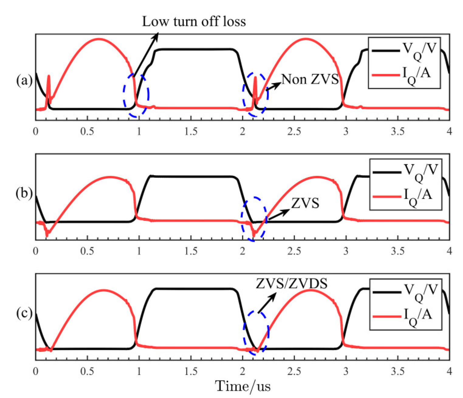
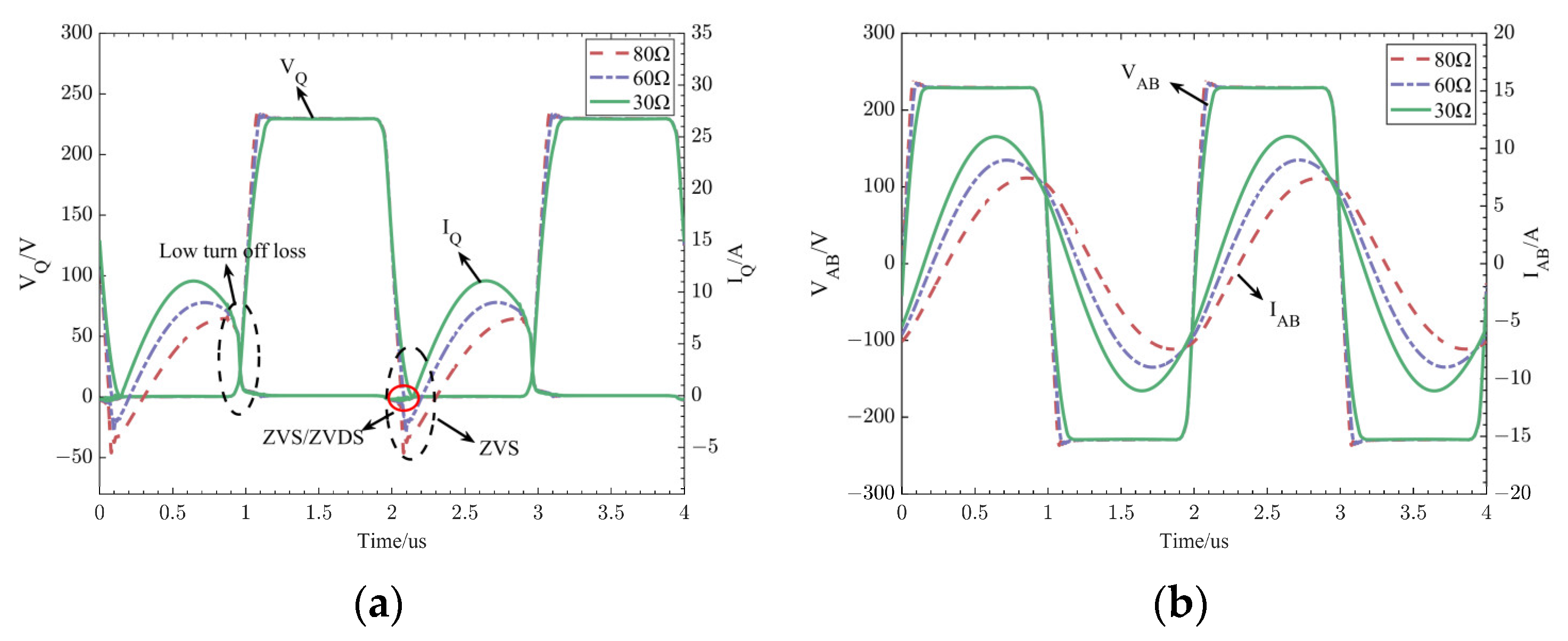
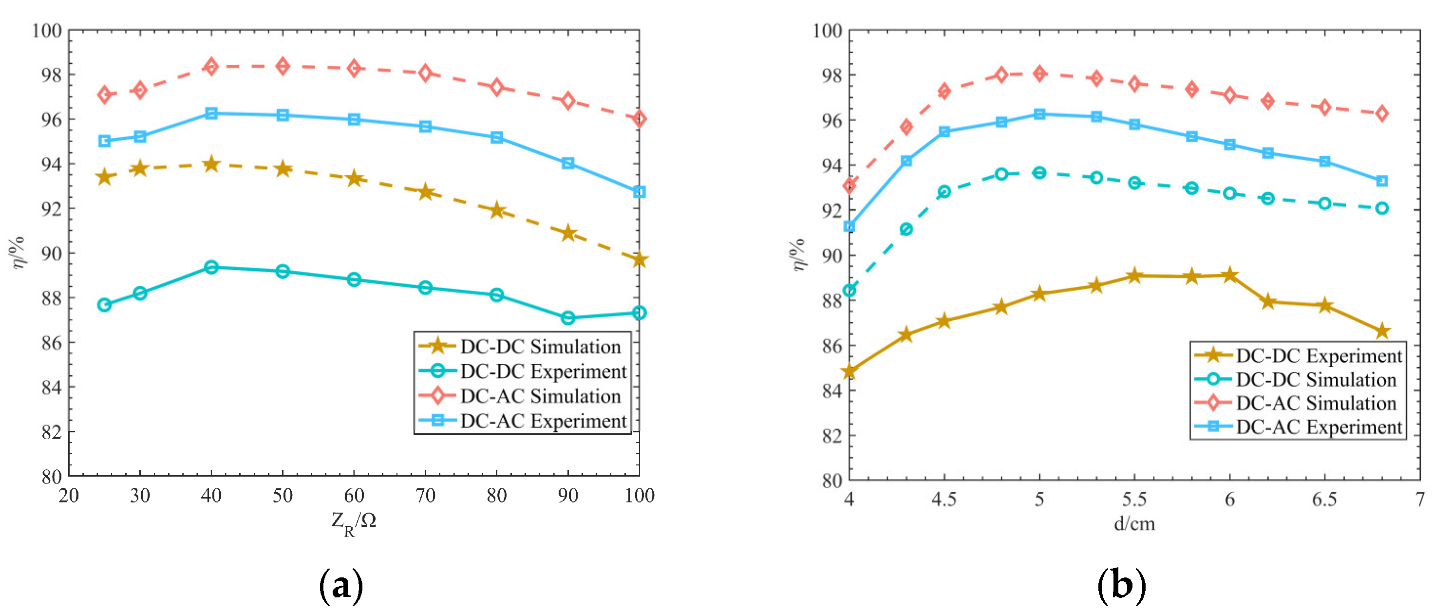
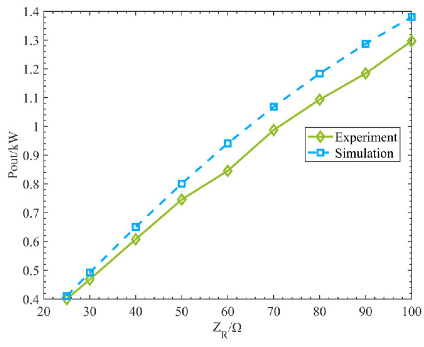
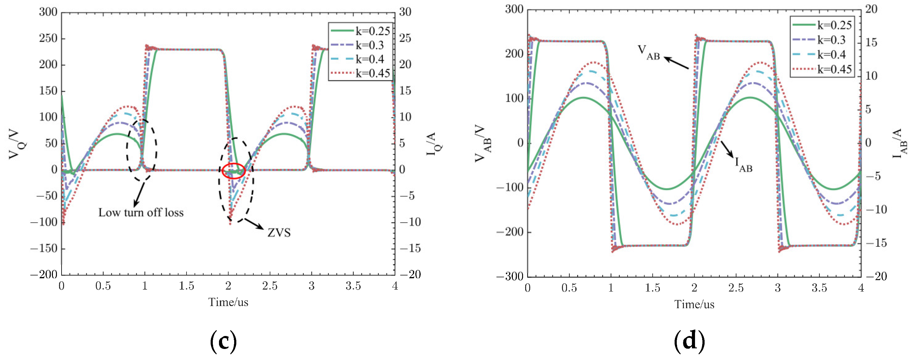
4.2. Simulation Verification

Based on the analysis above, the circuit simulation was constructed using Semitrix-SIMPLIS 8.3.Ink software, and only the switching losses were taken into account in the simulation. Each of the three working conditions was simulated in Semitrix simulation software. The first scenario involved a static wireless power transfer where the rectifier load ZR was varied from 30 Ω to 80 Ω. The second scenario included dynamic wireless power transfer with coupling coils position offset, where the impedance matching design method results in changes in the real and imaginary parts. The third case examined transmission for various power levels at optimal loads and distance of coupling coils.
In the first scenario, the simulation was conducted with the coupling coils in their optimal state while varying the load. According to Figure 11a, we can ensure that the Class DE inverter operates in the ZVS region when the equivalent load ZR varies from 30 Ω to 80 Ω. The turn-off of the MOSFET will reduce the turn-off loss caused by the capacitance Cs connected in parallel. Figure 11b shows the curves of the input voltage V A B and input current I A B for the load-varying resonant port AB. ZVS can be reached for all load variations, but the diode’s turn-on time is prolonged because of the excessively large initial phase. However, its overall efficiency is higher than that of hard switching. In the second case, coils change position. Figure 11c,d indicates that achieving ZVS characteristics with low turn-off losses is possible for Class DE inverters with coupling coefficients ranging from 0.25 to 0.45.
In conclusion, it is known from simulation and theory that the ZVS region occurs when ZR > 30 Ω and k > 0.25. The coil coupling factor and load become larger, causing the initial phase to increase, which will also prolong the diode conduction time and increase reactive power. Therefore, it is advisable to carefully select the appropriate value of C S during the design phase.

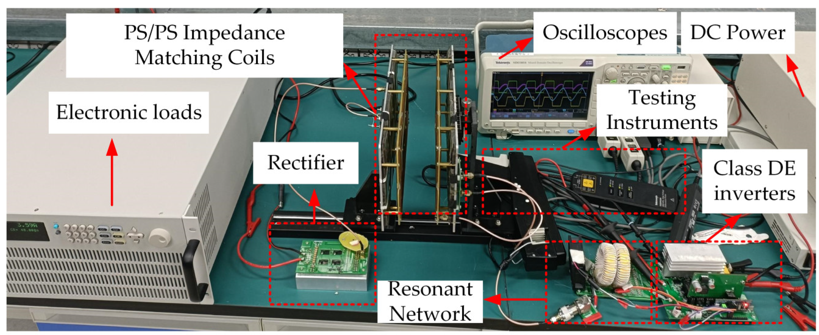
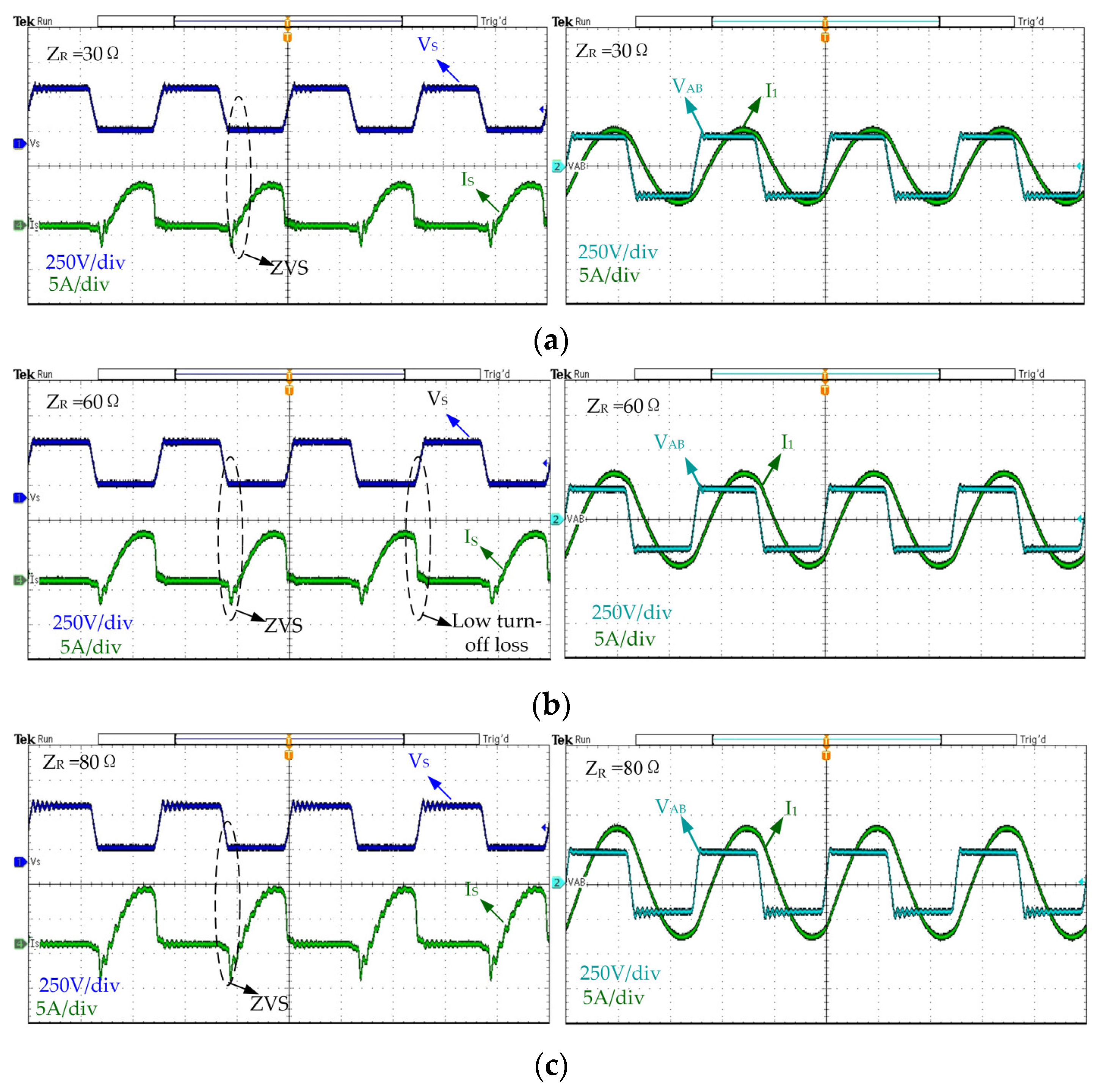
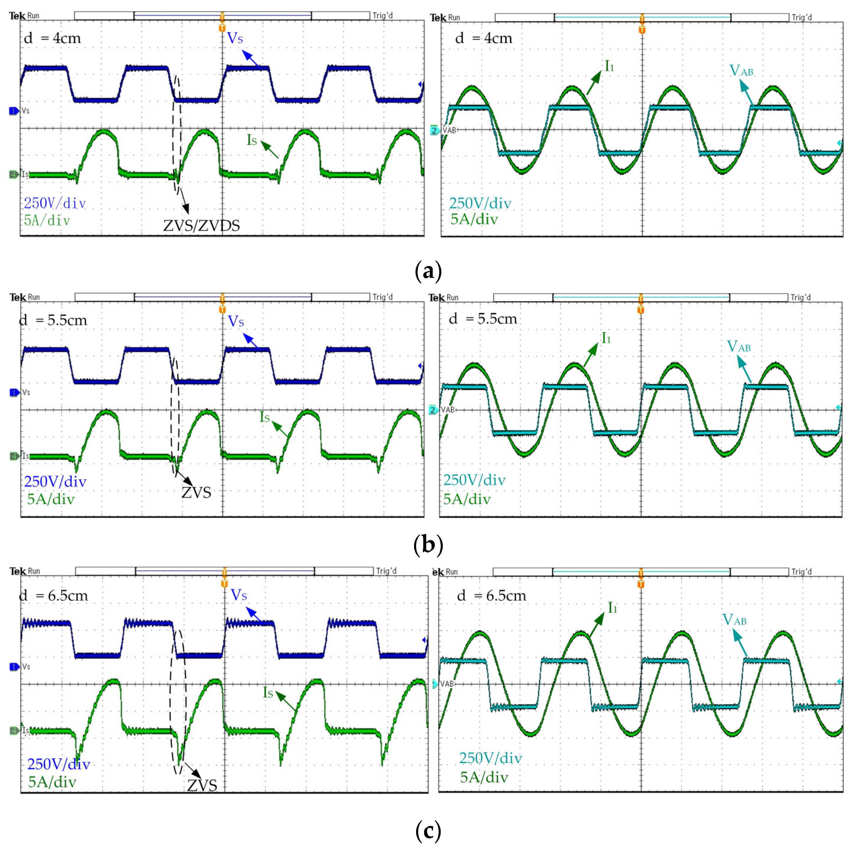
4.3. Experimental Verification

Figure 12 shows an experimental prototype of a 1 kW system constructed using the impedance-matching design method. In Figure 12, we measured the high-frequency AC output voltage of the Class DE inverter using a Tektronix THDP0200 high-voltage probe made by Tektronix in Beaverton, OR, USA, and the high-frequency AC output current using a HIOKI 3276 current probe made by HIOKI in Ueda, Nagano, Japan. The bandwidth of the voltage probe was 200 MHz, while the bandwidth of the current probe was 30 MHz. The operating frequency of the prototype is 500 kHz, so the accuracy of the voltage and current measurement instruments was good. For high-power and high-frequency power transfer, we calculated the efficiency of Class DE inverters by measuring the root mean square (RMS) values of voltage and current. However, the measurement accuracy of the current probe may be affected by nearly electromagnetic interference, and the voltage–current probe will produce the effect of temperature drift and other measurement errors. In fact, these effects are negligible. All MOSFETs and diodes are identical to those in the simulation, and the specific design parameters can be found in Table 2. To simulate load variations, the rectifier load was utilized as an adjustable electronic load based on the three different working conditions that were confirmed in the simulation mentioned earlier. For the first scenario, the DC input supply was fixed at 260 V, the coupling coil was aligned, and the equivalent load Z R was varied. An oscilloscope was used to measure the voltage and current curves of the MOSFETs in the Class DE inverter.
The ZVS curves and the voltage-current curves of the resonant network for the tested MOSFETs with load resistance Z R of 30 Ω, 60 Ω, and 80 Ω, respectively, are displayed in Figure 13a–c. We can observe that the inverter consistently followed the ZVS soft-switching characteristics and exhibited low turn-off losses based on the voltage-current curves of the MOSFETs. As the value of ZR increased, the initial phase angle of the input current to the AB port also increased, resulting in a longer time for it to pass through the body diode. The inverter exhibited ZVS characteristics, resulting in lower overall losses at high frequencies compared to the hard-switched state. This verifies the effectiveness of resonant network design for wide-load ZVS of inverters.
In the second scenario, experiments are conducted to observe changes in the real and imaginary parts of the impedance resulting from the coil position offset. The ZVS curves of the MOSFETs and the voltage-currents curves of the resonant network were tested at coil distances d of 4 cm, 5.5 cm, and 6.5 cm in Figure 14a–c. From Figure 14, it can be seen that the Class DE inverter operates in the ZVS state when the distance was varied from 4.5 cm to 6 cm. The initial phase angle of the input current to the AB port of the resonant network increased as the coil distance increased. This resulted in a longer time for the current to pass through the body diode, an increase in reactive power, and a reduction in efficiency.
Figure 15 shows that the trends in simulated and experimental efficiency were similar when the load and the distance between coupling coils were changed. In Figure 15a, ZR changed from 30 Ω to 80 Ω. We can see that the inverter efficiency was greater than 95%, with the highest efficiency being 97.3%, and the system efficiency consistently exceeded 87.5%. In Figure 15b, the coil distance d ranged from 4.5 to 6 cm. The efficiency of Class DE inverters is shown to be above 95% in Figure 15b, where the coil distance d varied from 4.5 to 6 cm. The highest efficiency, meanwhile, reached 96.3%. Additionally, the system efficiency was greater than 87%. Figure 15 also shows that the small phase shift angle and the small reactive power introduced were what caused the highest efficiency point to exist. Figure 16 illustrates the third test condition, showing that the system’s output power capability increased linearly with load variation. It also illustrates the direct introduction of the load into the load side of the inverter through impedance matching. It should be noted that the simulated passive components ware all ideal components. The actual efficiency of the system simulation is generally higher than the experimental efficiency. This is mainly because this paper focuses solely on the Class DE inverter and coupling coil compensation. The receiver-side rectifier in the experiment was not best matched or optimized.
This impedance-matching compensation method can be implemented using RF tools like vector network analyzers. From the impedance matching perspective, it is easier for us to adjust and optimize the coil to achieve the best impedance design conditions for the system. In the later stages, without communication, closed-loop control can be implemented through a secondary DC-DC converter to achieve a controllable and stable voltage output of the system. Variable compensation capacitors or phase shifts on the secondary side can be built to achieve Class DE inverters with full impedance ZVS and ZVDS characteristics.

5. Conclusions

This paper analyses the impedance characteristics of Class DE inverters under various operating conditions. In the WPT system, the proposed symmetrical PS/PS impedance matching design method is used to compensate for the coupling coils. Meanwhile, Class DE inverters are load-sensitive and have an optimum design load. It is more suitable for impedance matching. The impact of load and coil position variations on the impedance of Class DE inverters is detailed in the analysis of this paper. To overcome the sensitivity of Class DE inverter impedance, a proposed impedance transform resonant network is used to broaden the purely resistive ZVS operating region of Class DE inverters. Furthermore, the impact of resonant network and shunt capacitance parameters on the ZVS region of Class DE inverters is analyzed. To enhance the wide impedance perturbation capability of Class DE inverters, we can reasonably choose the parameters of the shunt capacitance, which also helps in lowering the turn-off losses. Finally, the article presents a comprehensive impedance-matching design process for WPT systems and validates it through experiments and simulations. A prototype WPT system was constructed, and the Class DE inverter can achieve soft-switching characteristics when ZR > 30 Ω or k > 0.25. The efficiency of Class DE inverter is over 95% when ZR ranges from 30 Ω to 80 Ω or d ranges from 4.5 cm to 6 cm. The system efficiency is greater than 87%. The output power had an approximate linear relationship with the load, and the load exhibited an approximately constant current characteristic. This paper is more informative for the system design of static wireless power transfer systems in specific applications.

Author Contributions

Conceptualization, P.W. and Q.L.; methodology, Q.L.; software, P.W.; validation, Y.L., W.Y. and K.Y.; formal analysis, Z.P.; investigation, Q.L.; resources, Y.L.; data curation, W.Y.; writing—original draft preparation, P.W.; writing—review and editing, Q.L. and W.Y.; supervision, Y.L. All authors have read and agreed to the published version of the manuscript.

Funding

This research received no external funding.

Data Availability Statement

All the data supporting the reported results have been included in this paper.

Conflicts of Interest

The authors declare no conflicts of interest.

References

  1. Li, J.; Qin, R.; Sun, J.; Costinett, D. Systematic Design of a 100-W 6.78-MHz Wireless Charging Station Covering Multiple Devices and a Large Charging Area. IEEE Trans. Power Electron. 2022, 37, 4877–4889. [Google Scholar] [CrossRef]
  2. Cai, C.; Liu, X.; Wu, S.; Chen, X.; Chai, W.; Yang, S. A Misalignment Tolerance and Lightweight Wireless Charging System via Reconfigurable Capacitive Coupling for Unmanned Aerial Vehicle Applications. IEEE Trans. Power Electron. 2023, 38, 22–26. [Google Scholar] [CrossRef]
  3. Zhu, Q.; Wang, L.; Guo, Y.; Liao, C.; Li, F. Applying LCC Compensation Network to Dynamic Wireless EV Charging System. IEEE Trans. Ind. Electron. 2016, 63, 6557–6567. [Google Scholar] [CrossRef]
  4. Inoue, K.; Kusaka, K.; Itoh, J.-I. Reduction in Radiation Noise Level for Inductive Power Transfer Systems Using Spread Spectrum Techniques. IEEE Trans. Power Electron. 2018, 33, 3076–3085. [Google Scholar] [CrossRef]
  5. Luo, Z.; Wei, X. Analysis of Square and Circular Planar Spiral Coils in Wireless Power Transfer System for Electric Vehicles. IEEE Trans. Ind. Electron. 2018, 65, 331–341. [Google Scholar] [CrossRef]
  6. Ukita, K.; Kashiwagi, T.; Sakamoto, Y.; Sasakawa, T. Evaluation of a Non-Contact Power Supply System with a Figure-of-Eight Coil for Railway Vehicles. In Proceedings of the 2015 IEEE PELS Workshop on Emerging Technologies: Wireless Power (2015 WoW), Daejeon, Republic of Korea, 5–6 June 2015; pp. 1–6. [Google Scholar]
  7. Waters, B.H.; Sample, A.P.; Bonde, P.; Smith, J.R. Powering a Ventricular Assist Device (VAD) With the Free-Range Resonant Electrical Energy Delivery (FREE-D) System. Proc. IEEE 2012, 100, 138–149. [Google Scholar] [CrossRef]
  8. Tang, S.C.; Lun, T.L.T.; Guo, Z.; Kwok, K.-W.; McDannold, N.J. Intermediate Range Wireless Power Transfer With Segmented Coil Transmitters for Implantable Heart Pumps. IEEE Trans. Power Electron. 2017, 32, 3844–3857. [Google Scholar] [CrossRef]
  9. Wang, W.; Hemour, S.; Wu, K. Coupled Resonance Energy Transfer Over Gigahertz Frequency Range Using Ceramic Filled Cavity for Medical Implanted Sensors. IEEE Trans. Microw. Theory Techn. 2014, 62, 956–964. [Google Scholar] [CrossRef]
  10. Yang, L.; Ju, M.; Zhang, B. Bidirectional Undersea Capacitive Wireless Power Transfer System. IEEE Access 2019, 7, 121046–121054. [Google Scholar] [CrossRef]
  11. Mai, R.; Yan, Z.; Chen, Y.; Liu, S.; He, Z. A Hybrid Transmitter-Based Efficiency Improvement Controller with Full-Bridge Dual Resonant Tank for Misalignment Condition. IEEE Trans. Power Electron. 2020, 35, 1124–1135. [Google Scholar] [CrossRef]
  12. Li, H.; Li, J.; Wang, K.; Chen, W.; Yang, X. A Maximum Efficiency Point Tracking Control Scheme for Wireless Power Transfer Systems Using Magnetic Resonant Coupling. IEEE Trans. Power Electron. 2014, 30, 3998–4008. [Google Scholar] [CrossRef]
  13. Li, H.; Wang, K.; Fang, J.; Tang, Y. Pulse Density Modulated ZVS Full-Bridge Converters for Wireless Power Transfer Systems. IEEE Trans. Power Electron. 2018, 34, 369–377. [Google Scholar] [CrossRef]
  14. Stankiewicz, J.M. Estimation of the Influence of the Coil Resistance on the Power and Efficiency of the WPT System. Energies 2023, 16, 6210. [Google Scholar] [CrossRef]
  15. Prengel, S.; Helwig, M.; Modler, N. Lightweight Coil for Efficient Wireless Power Transfer: Optimization of Weight and Efficiency for WPT Coils. In Proceedings of the 2014 IEEE Wireless Power Transfer Conference (WPTC), Jeju, Republic of Korea, 8–9 May 2014. [Google Scholar]
  16. Sohn, Y.H.; Choi, B.H.; Lee, E.S.; Lim, G.C.; Cho, G.-H.; Rim, C.T. General Unified Analyses of Two-Capacitor Inductive Power Transfer Systems: Equivalence of Current-Source SS and SP Compensations. IEEE Trans. Power Electron. 2015, 30, 6030–6045. [Google Scholar] [CrossRef]
  17. Chowdary, K.V.V.S.R.; Kumar, K.; Banerjee, S.; Kumar, R.R. Comparative Analysis between High-Order Compensation and SS-Compensation for Dynamic Wireless Power Transfer System. In Proceedings of the 2020 IEEE International Conference on Power Electronics, Drives and Energy Systems (PEDES), Jaipur, India, 16–19 December 2020; pp. 1–6. [Google Scholar]
  18. Zhang, W.; Tse, C.K.; Chen, Q. Load-Independent Duality of Current and Voltage Outputs of a Series- or Parallel-Compensated Inductive Power Transfer Converter With Optimized Efficiency. IEEE J. Emerg. Sel. Top. Power Electron. 2015, 3, 137–146. [Google Scholar] [CrossRef]
  19. Yang, L.; Jiang, S.; Wang, C.; Shi, Y.; Wang, M.; Cai, C.; Zhang, L. A High-Efficiency Integrated LCC/S WPT System with Constant Current Output. IEEE J. Emerg. Sel. Top. Power Electron. 2023, 341–354. [Google Scholar] [CrossRef]
  20. Wang, Y.; Yao, Y.; Liu, X.; Xu, D.; Cai, L. An LC/S Compensation Topology and Coil Design Technique for Wireless Power Transfer. IEEE Trans. Power Electron. 2018, 33, 2007–2025. [Google Scholar] [CrossRef]
  21. Li, S.; Li, W.; Deng, J.; Nguyen, T.D.; Mi, C.C. A Double-Sided LCC Compensation Network and Its Tuning Method for Wireless Power Transfer. IEEE Trans. Veh. Technol. 2015, 64, 2261–2273. [Google Scholar] [CrossRef]
  22. Chen, L.; Liu, S.; Zhou, Y.C.; Cui, T.J. An Optimizable Circuit Structure for High-Efficiency Wireless Power Transfer. IEEE Trans. Ind. Electron. 2013, 60, 339–349. [Google Scholar] [CrossRef]
  23. Fereshtian, A.; Ghalibafan, J.; Koohestani, M. A Comprehensive Design Analysis of a Cost-Effective WPT System with a Class-E Power Amplifier and a T-Matching Network. AEU–Int. J. Electron. Commun. 2021, 137, 153826. [Google Scholar] [CrossRef]
  24. Liu, S.; Liu, M.; Yang, S.; Ma, C.; Zhu, X. A Novel Design Methodology for High-Efficiency Current-Mode and Voltage-Mode Class-E Power Amplifiers in Wireless Power Transfer Systems. IEEE Trans. Power Electron. 2016, 32, 4514–4523. [Google Scholar] [CrossRef]
  25. Fu, M.; Yin, H.; Liu, M.; Ma, C. Loading and Power Control for a High-Efficiency Class E PA-Driven Megahertz WPT System. IEEE Trans. Ind. Electron. 2016, 63, 6867–6876. [Google Scholar] [CrossRef]
  26. Liang, J.; Liao, W.-H. Steady-State Simulation and Optimization of Class-E Power Amplifiers with Extended Impedance Method. IEEE Trans. Circuits Syst. I 2011, 58, 1433–1445. [Google Scholar] [CrossRef]
  27. Jiang, Y.; Li, H.; Liu, Y.; Liang, J.; Wang, H.; Fu, M. Multiconstraint Design of Single-Switch Resonant Converters Based on Extended Impedance Method. IEEE J. Emerg. Sel. Top. Power Electron. 2023, 11, 1901–1912. [Google Scholar] [CrossRef]
  28. Abbasian, S.; Johnson, T. Power-Efficiency Characteristics of Class-F and Inverse Class-F Synchronous Rectifiers. IEEE Trans. Microw. Theory Techn. 2016, 64, 4740–4751. [Google Scholar] [CrossRef]
  29. Jedi, H.; Salvatierra, T.; Ayachit, A.; Kazimierczuk, M.K. High-Frequency Single-Switch ZVS Gate Driver Based on a Class ∅2 Resonant Inverter. IEEE Trans. Ind. Electron. 2020, 67, 4527–4535. [Google Scholar] [CrossRef]
  30. Kaczmarczyk, Z. High-Efficiency Class E, Class EF2, and Class E/F3 Inverters. IEEE Trans. Ind. Electron. 2006, 53, 1584–1593. [Google Scholar] [CrossRef]
  31. Samanta, S.; Rathore, A.K. Wireless Power Transfer Technology Using Full-bridge Current-fed Topology for Medium Power Applications. IET Power Electron. 2016, 9, 1903–1913. [Google Scholar] [CrossRef]
  32. Jiang, L.; Costinett, D. A High-Efficiency GaN-Based Single-Stage 6.78 MHz Transmitter for Wireless Power Transfer Applications. IEEE Trans. Power Electron. 2019, 34, 7677–7692. [Google Scholar] [CrossRef]
  33. Tebianian, H.; Salami, Y.; Jeyasurya, B.; Quaicoe, J.E. A 13.56-MHz Full-Bridge Class-D ZVS Inverter With Dynamic Dead-Time Control for Wireless Power Transfer Systems. IEEE Trans. Ind. Electron. 2020, 67, 1487–1497. [Google Scholar] [CrossRef]
  34. De Rooij, M. Performance Comparison for A4WP Class-3 Wireless Power Compliance between eGaN® FET and MOSFET in a ZVS Class D Amplifier. In Proceedings of the PCIM Europe 2015, International Exhibition and Conference for Power Electronics, Intelligent Motion, Renewable Energy and Energy Management, Nuremberg, Germany, 19–20 May 2015; pp. 1–8. [Google Scholar]
  35. De Rooij, M.; Zhang, Y. eGaN® FET Based 6.78 MHz Differential-Mode ZVS Class D AirFuelTM Class 4 Wireless Power Amplifier. In Proceedings of the International Exhibition and Conference for Power Electronics, Intelligent Motion, Renewable Energy and Energy Management, Nuremberg, Germany, 9–11 September 2016; pp. 1–8. [Google Scholar]
  36. Chung, E.; Ha, J.I. Impedance Matching Network Design for 6.78-MHz Wireless Power Transfer System With Constant Power Characteristics Against Misalignment. IEEE Trans. Power Electron. 2023, 39, 1788–1801. [Google Scholar] [CrossRef]
  37. Han, Y.; Leitermann, O.; Jackson, D.A.; Rivas, J.M.; Perreault, D.J. Resistance Compression Networks for Radio-Frequency Power Conversion. IEEE Trans. Power Electron. 2007, 22, 41–53. [Google Scholar] [CrossRef]
  38. Issi, F.; Kaplan, O. Design and Application of Wireless Power Transfer Using Class-E Inverter Based on Adaptive Impedance-Matching Network. ISA Trans. 2022, 126, 415–427. [Google Scholar] [CrossRef] [PubMed]
  39. Owais, M. Deep Learning for Integrated Origin–Destination Estimation and Traffic Sensor Location Problems. IEEE Trans. Intell. Transp. Syst. 2024, 1–13. [Google Scholar] [CrossRef]
  40. Owais, M.; Alshehri, A.; Gyani, J.; Aljarbou, M.H.; Alsulamy, S. Prioritizing Rear-End Crash Explanatory Factors for Injury Severity Level Using Deep Learning and Global Sensitivity Analysis. Expert Syst. Appl. 2024, 245, 123114. [Google Scholar] [CrossRef]
  41. Koizumi, H.; Suetsugu, T.; Fujii, M.; Shinoda, K.; Mori, S.; Iked, K. Class DE High-Efficiency Tuned Power Amplifier. IEEE Trans. Circuits Syst. I 1996, 43, 51–60. [Google Scholar] [CrossRef]
  42. Wei, X.; Sekiya, H.; Nagashima, T.; Kazimierczuk, M.K.; Suetsugu, T. Steady-State Analysis and Design of Class-D ZVS Inverter at Any Duty Ratio. IEEE Trans. Power Electron. 2016, 31, 394–405. [Google Scholar] [CrossRef]
  43. Sarnago, H.; Lucía, Ó.; Mediano, A.; Burdío, J.M. Class-D/DE Dual-Mode-Operation Resonant Converter for Improved-Efficiency Domestic Induction Heating System. IEEE Trans. Power Electron. 2013, 28, 1274–1285. [Google Scholar] [CrossRef]
  44. Albertoni, L.; Grasso, F.; Matteucci, J.; Piccirilli, M.C.; Reatti, A.; Ayachit, A.; Kazimierczuk, M.K. Analysis and Design of Full-Bridge Class-DE Inverter at Fixed Duty Cycle. In Proceedings of the IECON 2016—42nd Annual Conference of the IEEE Industrial Electronics Society, Florence, Italy, 23–26 October 2016; pp. 5609–5614. [Google Scholar]
  45. Inoue, K.; Nagashima, T.; Wei, X.; Sekiya, H. Design of High-Efficiency Inductive-Coupled Wireless Power Transfer System with Class-DE Transmitter and Class-E Rectifier. In Proceedings of the IECON 2013—39th Annual Conference of the IEEE Industrial Electronics Society, Vienna, Austria, 10–13 November 2013; pp. 613–618. [Google Scholar]
  46. Krishna, A.V.; Rashmi, M.R. Wireless Power Transfer for LED Display System Using Class-DE Inverter. In Emerging Research in Electronics, Computer Science and Technology; Sridhar, V., Padma, M.C., Rao, K.A.R., Eds.; Springer: Singapore, 2019; pp. 1271–1282. [Google Scholar]
  47. Yusop, Y.; Saat, S.; Kamarudin, K.; Husin, H.; Nguang, S.K. Π1a and Π1b Impedance Matching for Capacitive Power Transfer System. In Embracing Industry 4.0; Lecture Notes in Electrical Engineering; Mohd Razman, M.A., Mat Jizat, J.A., Mat Yahya, N., Myung, H., Zainal Abidin, A.F., Abdul Karim, M.S., Eds.; Springer: Singapore, 2020; Volume 678, pp. 227–249. [Google Scholar]
  48. Pellitteri, F.; Boscaino, V.; Di Tommaso, A.O.; Miceli, R.; Capponi, G. Experimental Test on a Contactless Power Transfer System. In Proceedings of the 2014 Ninth International Conference on Ecological Vehicles and Renewable Energies (EVER), Monte-Carlo, Monaco, 25–27 March 2014; pp. 1–6. [Google Scholar]
  49. Huang, X.; Lu, C.; Liu, M. Calculation and Analysis of Near-Field Magnetic Spiral Metamaterials for MCR-WPT Application. Appl. Phys. A 2020, 126, 1–9. [Google Scholar] [CrossRef]
Figure 1. Class DE wireless power transfer system.
Electronics 13 00959 g001
Figure 2. Symmetrical PS/PS impedance matching compensation topology.
Electronics 13 00959 g002
Figure 3. Effect of variation of k and ZR on input impedance Zin: (a) effect of k and ZR on the real part of Zin, (b) effect of k and ZR on the imaginary part of Zin.
Electronics 13 00959 g003
Figure 4. Voltage gain curve.
Electronics 13 00959 g004
Figure 5. Equivalent circuit of π1a impedance-matched resonant network for Class DE inverter: (a) π1a matched resonant circuit, (b) π1a matched resonant equivalent circuit.
Electronics 13 00959 g005
Figure 6. ZVS voltage and current waveforms: (a) In first state, MOSFETs can’t attain the ZVS characteristic, (b) In second state, MOSFETs can attain the ZVS characteristic, (c) In third state, MOSFETs can attain both the ZVS and ZVDS characteristics.
Electronics 13 00959 g006
Figure 7. Impedance characteristics of π1a matching network.
Electronics 13 00959 g007
Figure 8. Variation of coil alignment load ZR and variation of CS with different ZVS ranges.
Electronics 13 00959 g008
Figure 9. Effect of coil offset on resonant network Xr and RS: (a) coil offset reflected impedance causes Xr change, and (b) coil offset reflected impedance causes RS change.
Electronics 13 00959 g009
Figure 10. Effect of different values of the C S parameter on the ZVS region under coil offset.
Electronics 13 00959 g010
Figure 11. Load and coupling factor variation ZVS curves: (a) load variation ZVS curve, (b) load change port AB voltage-current curve, (c) ZVS curve for variation of coupling factor k, and (d) AB voltage-current curves for ports with varying coupling factor k.
Electronics 13 00959 g011aElectronics 13 00959 g011b
Figure 12. Experimental prototype platform.
Electronics 13 00959 g012
Figure 13. Load variation ZVS curve and input voltage-current curve: (a) test curve for load equal to 30 Ω, (b) test curve for load equal to 60 Ω, and (c) test curve for load equal to 80 Ω.
Electronics 13 00959 g013
Figure 14. Coil position offset ZVS curve and input and output voltage and current curves: (a) coupling coil distance d = 4 cm test curve, (b) coupling coil distance d = 5.5 cm test curve, and (c) coupling coil distance d = 6.5 cm test curve.
Electronics 13 00959 g014
Figure 15. Efficiency curves for load and coupling factor variation: (a) load variation efficiency curve, and (b) coupling factor variation efficiency curve.
Electronics 13 00959 g015
Figure 16. Variation curve of output power capacity.
Electronics 13 00959 g016
Table 1. Class DE inverter working state.
Operation ModesSwitching Status
Q1Q2Q3Q4
0 < θ < 2πD
ONOFFOFFON
2πD <θ < π
OFFOFFOFFOFF
π< θ < π + 2πD
OFFONONOFF
π + 2πD < θ < 2π
OFFOFFOFFOFF
Table 2. System parameter design.
SymbolParameterValue
kCoil coupling coefficient0.3
αShunt capacitance factor0.85
φInitial phase shift capacitance2.82 rad
C1compensation series capacitance5.36 nF
C2compensated shunt capacitance6.32 nF
CPcompensated shunt capacitance12.43 nF
L1/L2Primary and secondary inductance27.3 μH
RLLoad resistance35~110 Ω
LInverter resonant cavity inductance40.23 μH
DDuty cycle0.423
QQuality factor5.05
CSMOSFET parallel total capacitance1.2 nF
f0Operating frequency500 kHz
Caresonant compensation capacitance3.776 nF
Disclaimer/Publisher’s Note: The statements, opinions and data contained in all publications are solely those of the individual author(s) and contributor(s) and not of MDPI and/or the editor(s). MDPI and/or the editor(s) disclaim responsibility for any injury to people or property resulting from any ideas, methods, instructions or products referred to in the content.

