Communication

Simulation Study of 4H-SiC Low Turn-Off Loss and Snapback-Free Reverse-Conducting Gate Turn-Off Thyristor with N-Float Structure

1
Institute of Electronics Engineering, China Academy of Engineering Physics, Mianyang 621900, China
2
Microsystem and Terahertz Research Center, China Academy of Engineering Physics, Chengdu 610200, China
3
School of Integrated Circuits Science and Engineering, University of Electronic Science and Technology of China, Chengdu 610054, China
*
Author to whom correspondence should be addressed.
Electronics 2024, 13(4), 786; https://doi.org/10.3390/electronics13040786
Submission received: 18 January 2024 / Revised: 8 February 2024 / Accepted: 15 February 2024 / Published: 17 February 2024

Abstract

:
In this study, a novel integrated 4H-SiC reverse-conducting gate turn-off thyristor (GTO) featuring an N-type floating (NF) structure is proposed. The proposed NF-structured 4H-SiC GTO outperforms conventional reverse-conducting GTOs in forward conduction, effectively eliminating the snapback phenomenon. This is achieved by increasing lateral resistance above the P-injector and modifying the electron current path during early turn-on. NF structures with a doping concentration of 2 × 1014 cm−3 and thicknesses exceeding 4 μm have been indicated to successfully eliminate the snapback phenomenon. Moreover, the anode-shorted structure enhances the GTO’s breakdown voltage and concurrently reduces turn-off losses by 85% at low current densities.

1. Introduction

In recent years, advancements in power distribution and energy transmission applications, including smart grids, ultra-high voltage power transportation, and pulse power technology, have heightened the demand for high-voltage power devices [1,2,3,4]. Typically, conventional silicon (Si) power devices can withstand voltages up to 8 kV [5]. Beyond this limit, complex arrangements of converters or devices become necessary, especially in ultra-high voltage contexts [6,7]. This necessity has shifted the focus towards wide bandgap (WBG) semiconductors, particularly 4H-SiC, renowned for their superior material characteristics. 4H-SiC is increasingly favored for fabricating ultra-high voltage and high-frequency power devices because of its exceptional properties: a bandgap three times wider than that of silicon, a critical breakdown electrical field ten times higher, and an electron saturation velocity surpassing silicon by an order of magnitude [8,9].
In recent years, significant strides have been made in refining the SiC epitaxial growth process, marked by noteworthy advancements in enhancing charge carrier lifetimes and reducing bulk- and interface-trap densities. These improvements have been instrumental in achieving substantial progress in the development of high-voltage SiC devices. Wolfspeed (formerly known as Cree Inc., Durham, NC, USA) have announced their development of SiC MOSFETs with impressive blocking voltages of 10 kV and 15 kV [10]. Concurrently, there has been a technological breakthrough in bipolar devices rated above 20 kV, achieving PIN diodes with blocking voltages ranging from 7 to 39 kV, further pushing the boundaries in high-voltage device engineering [4,11]. In addition, 10 kV SBD and JBS diodes have also been produced [12]. In 2015, the voltage and current capabilities of SiC IGBTs saw a significant enhancement, reaching 27.5 kV/20 A [13]. In 2013, Cree Inc. advanced the SiC p-GTO’s performance to 20 kV [14], followed by the development of a 15 kV SiC n-GTO in 2019 [15]. Furthermore, in 2017, a SiC Emitter Turn-Off Thyristor (ETO) p-ETO with a blocking voltage of 22 kV was reported [16], exemplifying continued advancements in SiC device technology. Additionally, researchers are focusing on the stacking technology of SiC-based power devices for ultra-high voltage applications [17,18]. In the study referenced in [16], an assessment of the forward current handling capacities of 15 kV SiC GTO (p-type), IGBT, and MOSFET at temperatures of 25 °C and 125 °C was conducted. This analysis clearly indicates that the SiC GTO outperforms in terms of managing higher currents with the least forward voltage drop, marking it a key player for the next generation of ultra-high power devices. In the research documented in [19], simulation models were employed to validate that within a range of 20–50 kV, SiC GTOs exhibit a voltage drop of 3.4–7.8 V at a current density of 20 A/cm2 at room temperature, whereas IGBTs display a voltage drop between 4.2 and 10 V under similar conditions. The underlying reason for this enhanced performance of SiC GTO, from the viewpoint of semiconductor current conduction, is its capability for bidirectional carrier injection and pronounced conductivity modulation in the drift region. Therefore, the SiC GTO is emerging as a highly viable option for ultra-high voltage power applications.
However, the intense conductivity modulation effect leads to an increased turn-off time, subsequently slowing down the switching speed. In the case of GTO devices, turn-off losses constitute a major part of the overall switching losses, prompting considerable efforts in recent years to minimize these losses. To enhance GTO performance, various structures such as Integrated Gate-Commuted Thyristors (IGCT), Emitter Turn-Off (ETO) Thyristors, and Reverse-Conducting GTOs (RC-GTO) have been proposed [20,21,22]. The Reverse-Conducting GTO (RC-GTO) introduces an innovative design that combines a diode with a GTO at the cellular level. This integrated architecture functions as a high-voltage forward switch and, when reversed, operates as a continuous current diode [22,23,24,25]. Traditional GTOs, lacking reverse conduction capability, necessitate parallel connection with a reverse diode. Thus, compared to conventional GTOs, RC-GTOs offer enhanced power density, streamlined system design, and improved thermal cycling of the chip. However, like RC-IGBTs, conventional RC-GTOs suffer from an undesirable snapback effect, which hinders the device from fully turning on [26]. In this study, a novel integrated SiC Reverse-Conducting GTO (RC-GTO) structure featuring an N-type floating region (NF-RC-GTO) is presented. This design effectively suppresses and eliminates the snapback phenomenon, minimally impacting the primary performance. Additionally, it features low turn-off loss at low current densities.

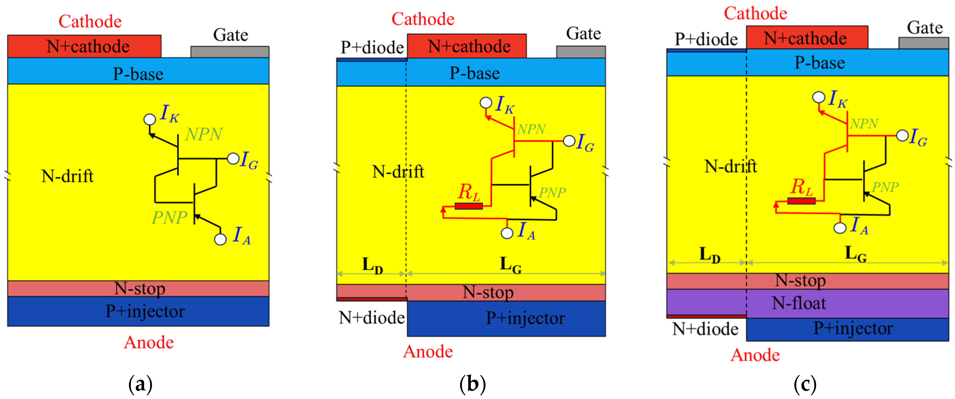
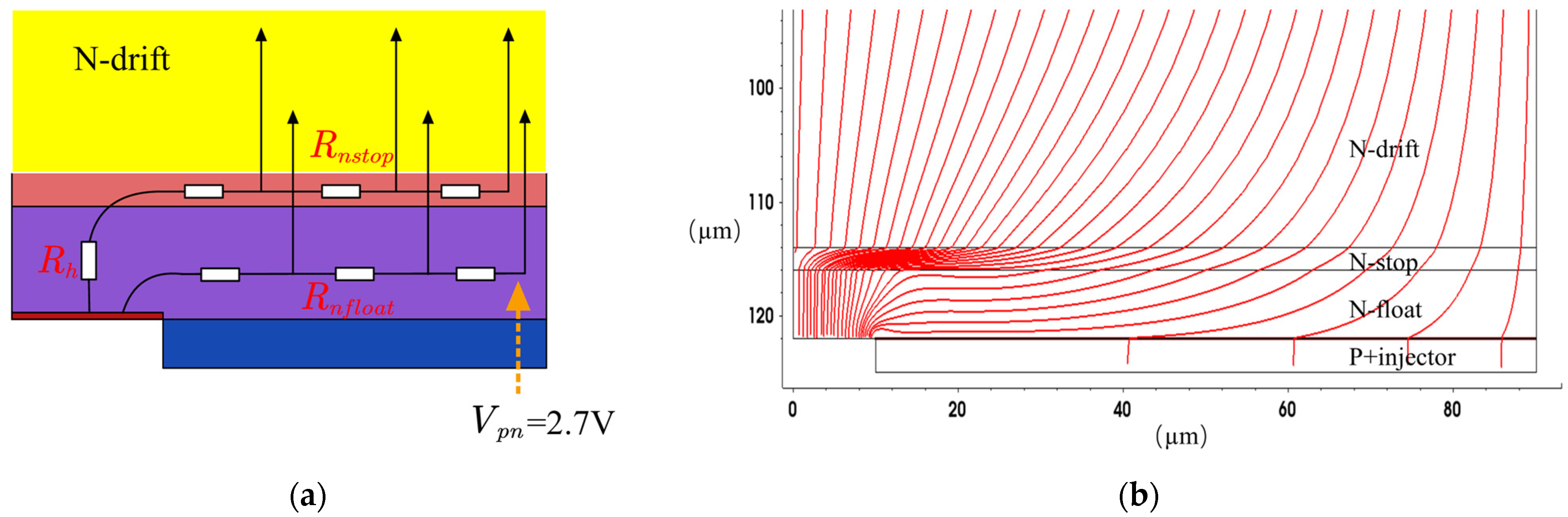
2. Device Structure and Mechanism
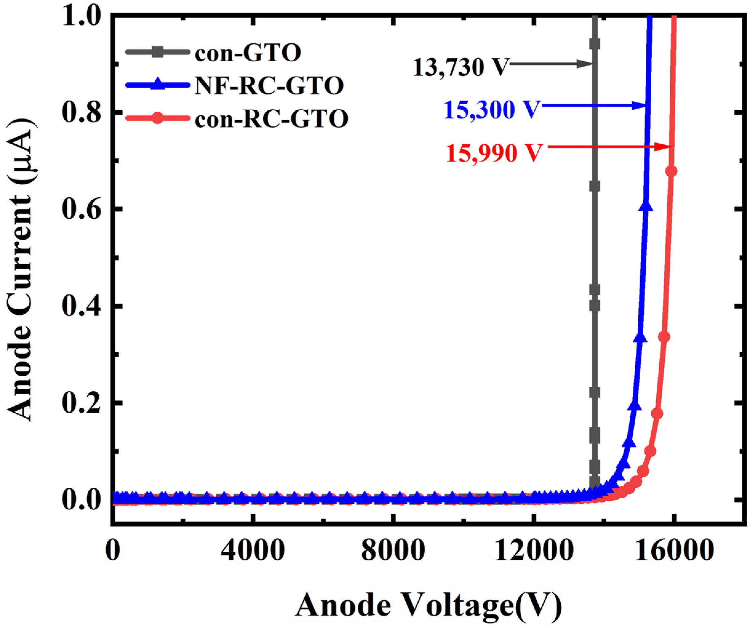
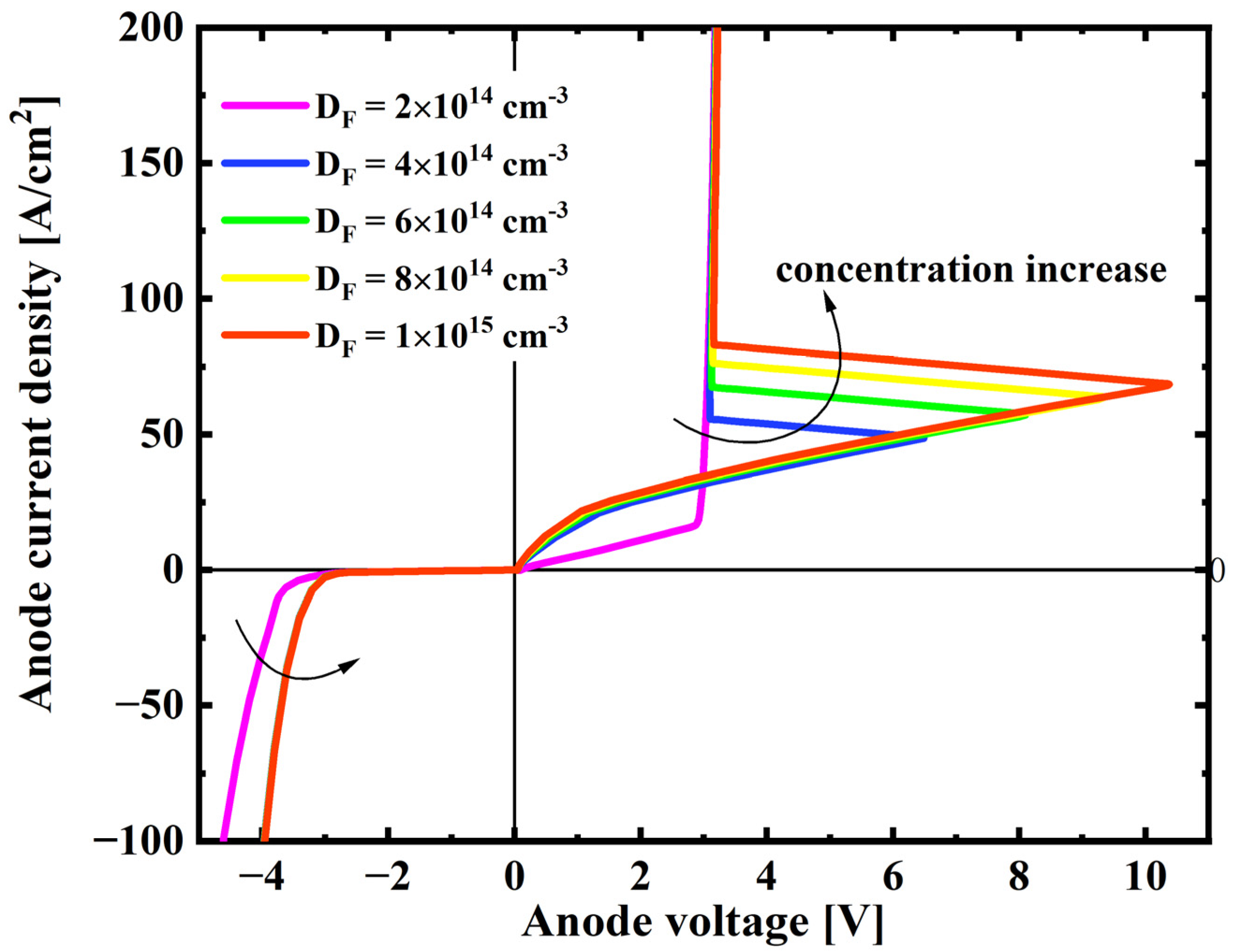
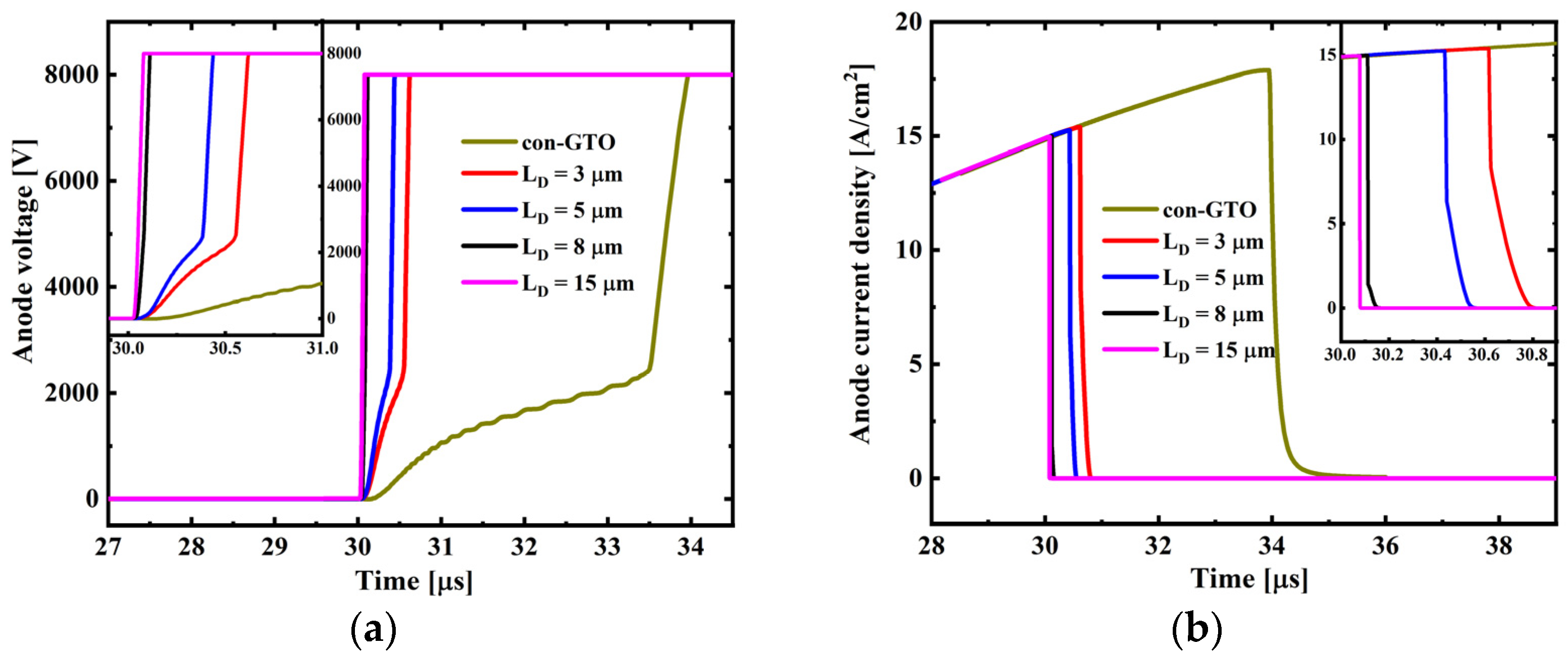
Figure 1a–c illustrate the simulation structures and equivalent circuit diagrams of the GTO, conventional RC-GTO (con-RC-GTO), and NF-RC-GTO, respectively. The SiC GTO is comprised of five layers: p-n-n-p-n, which functionally resemble two back-to-back PNP and NPN bipolar junction transistors (BJTs). The currents in these two BJTs are interdependent, and the device activates when the sum of the common-base current gains, denoted as αPNP and αPNP for the PNP and NPN BJTs, respectively, exceeds 1 [27,28]. Compared to a standard GTO, both the conventional RC-GTO (con-RC-GTO) and the NF-RC-GTO feature an anode-shortened structure and a cathode-shortened structure, functioning as a reverse diode. In the equivalent circuit of a SiC RC-GTO, the additional connection to the N-drift region is modeled as a resistor (RL) placed parallel between the base and emitter terminals of the inherent PNP bipolar transistor (BJT). RL is nonlinear, primarily determined by the shape and doping concentration of the N-stop (and for NF-RC-GTO, also the N-float) regions. During the initial phase of forward-conduction mode, the RC-GTO operates akin to an NPN BJT. This continues until the conduction current is sufficient to cause the voltage drop across RL to exceed 2.7 V, which is approximately the turn-on threshold voltage of a conventionally doped SiC PN junction at room temperature, fully activating the emitter-base junction of the inherent PNP transistor. Once activated, the inherent PNP transistor contributes to conductivity modulation in the N-drift region, leading to a significant decrease in the resistance between the cathode and anode of the device. Subsequently, the RC-GTO transitions to operate as a conventional GTO. This shift from NPN BJT to GTO operation is marked by a voltage jump and an exponential increase in anode current, a process known as the snapback phenomenon [29,30,31].
To mitigate the snapback effect, the NF-RC-GTO incorporates an additional N-float layer with a lower doping concentration (such as 2 × 1014 cm−3). This layer boosts the lateral resistance above the P-injector, directing current flow through areas of higher resistance and enabling the emitter-base junction of the intrinsic PNP bipolar transistor to activate at much lower currents. It is important to note the symmetrical relation of the cathode-shortened region to the gate structure in the NF-RC-GTO, which simplifies the formation of the cathode-shortened structure, especially when compared to traditional SiC-nGTO fabrication processes [32].
The performance of the various structures was simulated using Synopsys Sentaurus Technology Computer-Aided Design software, which computes fundamental physical partial differential equations and physical models, such as the Poisson equation and diffusion and transport equations, to facilitate the simulation of the structure and electrical characteristics of semiconductor devices. Please note, all subsequent results are derived from simulation experiments. The basic physical models utilized in the TCAD simulations encompass impact ionization, incomplete ionization, Shockley–Read–Hall and Auger recombination, doping concentration-dependent carrier lifetime, and electric field and doping concentration-dependent carrier mobility [33,34]. The average lifetimes of carriers are defined as 2.5 µs for electrons and 0.5 µs for holes [32], which align with values commonly found in commercially available epitaxial layer structures [14,35]. The standard parameters for the 13 kV SiC NF-RC-GTO, SiC con-RC-GTO, and con-GTO are compiled and presented in Table 1.
Figure 2 displays the current–voltage (I–V) characteristics for the GTO, con-RC-GTO, and NF-RC-GTO. In terms of forward turn-on performance, the conventional GTO exhibits optimal characteristics with a smooth transition, notably absent of any snapback effect [36]. For the RC-GTO variants, prior to the turn-on of the anode P/N diode, the devices exhibit behavior akin to an NPN BJT, a result of the additional electron excess provided by the N+ diode region. Specifically, in the case of the con-RC-GTO, a broader LG dimension diminishes the snapback effect. As LG widens from 110 μm to 120 μm, there is a notable reduction in the snapback voltage from 6.11 V down to 4.83 V. Conversely, the NF-RC-GTO sees the complete elimination of the snapback effect with a reduced LG width of just 80 μm, affirming the effectiveness of the N-float structure in mitigating this issue. Furthermore, the forward conduction voltage drop (measured at a current density of 100 A/cm2) is comparable to that of the con-RC-GTO. It is important to consider that an oversized LG dimension may lead to an uneven distribution of current within the device. This imbalance can result in thermal concentration issues, and additionally, it has the potential to diminish the available space for the reverse PN diode structure [32].
Figure 3 illustrates the initial paths of electron and hole currents during the conduction mode. Specifically, Figure 3a depicts the flow of electron current into the P-collector, bypassing the N-stop layer and entering the N-float layer in the NF-RC-IGBT under unipolar mode. This dual-layer structure effectively channels the current flow through the N-float region, significantly increasing the path resistance [30]. The current flow lines shown in Figure 3b confirm this. The voltage across the P-injector and N-float junction, distant from the N region, reaches at least 2.7 V at the earliest stage. Subsequently, the P-injector at this juncture begins to inject holes, facilitating conductivity modulation. Consequently, the device transitions into operating as a GTO.
The simple snapback model [30,37] used for Figure 3a can be described as follows:
V t o t = I R n f l o a t R n s t o p + R h R n f l o a t + R n s t o p + R h + V o t h e r
For the NF-RC-GTO, the N-float layer is pivotal in directing the current flow through areas of high resistance. This underscores the necessity for meticulous design of both the doping concentration and the geometry of the N-float region to more effectively suppress the snapback phenomenon.

3. Results

Figure 4 displays the characteristic curves of the forward off-state breakdown voltage. The breakdown voltages for the NF-RC-GTO, con-RC-GTO, and con-GTO are 15,303 V, 15,992 V, and 13,730 V, respectively. Both the NF-RC-GTO and con-RC-GTO, featuring an anode-short structure, exhibit higher breakdown voltages compared to the conventional GTO. Notably, the NF-RC-GTO shows an 11.4% improvement over the con-GTO. This enhanced performance is attributed to the anode-short circuit structure, which allows leakage current from the reverse-biased junction to directly exit through the short-circuited anode. This mechanism also prevents hole injection at the P+ injector region, reducing the common-base current gain of the anode PNP BJT, thereby increasing the forward breakdown voltage [38]. The slightly lower breakdown voltage of the NF-RC-GTO, compared to the con-RC-GTO, is due to the NF structure, which results in a shorter ndrift structure (104 µm).
Figure 5 provides insight into the effect of doping concentration in the float region on the forward and reverse performance of NF-RC-GTOs, which are characterized by a consistent thickness of 4 μm and an LG length of 80 μm. The figure reveals that as the doping concentration decreases, the snapback voltage also reduces, and the snapback phenomenon completely vanishes at a doping concentration of 2 × 1014 cm−3. This trend can be attributed to the increased lateral resistance above the P-injector resulting from the lower doping concentration, consequently leading to a reduced snapback voltage. Additionally, during the initial turn-on phase, the current in the NPN mode diminishes as the lateral resistance increases. It is also observed that with a higher doping concentration, the current handling capability slightly decreases. This is due to an increase in the compound current within the NF region, which negatively affects the hole injection efficiency in the anode region.
Figure 6 delineates the impact of the N-float structure’s thickness on the forward and reverse performance of NF-RC-GTOs. These devices share a consistent doping concentration and LG dimension for the N-float structure, at 2 × 1014 cm−3 and 80 μm, respectively. The figure indicates that the snapback voltage decreases with an increase in the thickness of the N-float structure. Notably, the snapback phenomenon is eliminated when the thickness exceeds 3 μm. This effect can be attributed to the thicker N-float structure reducing the direct flow of NPN mode current through the N-stop region to the anode-short structure during the initial turn-on phase. As a result, a higher proportion of electrons flow through the N-float region to the anode-short structure, facilitating earlier hole injection in the anode P-injector/N-float region [31,37]. Furthermore, Figure 6 also reveals that variations in the thickness of the N-float structure within a certain range do not significantly affect the NF-RC-GTO’s forward and reverse high-current handling capability.
The transient characteristics of the newly proposed NF-RC-GTO, with varying widths of the Anode-shortened structure (LD), are analyzed during the turn-off processes. A double pulse test (DPT) circuit is employed for evaluating the dynamic switching performance. The DPT setup includes a high-voltage DC power supply of 8000 V, a gate resistor of 5 Ω, a clamped inductive load of 5 mH, and a gate signal of 15 V/−100 V to provide sufficient gate trigger current. At t = 0, the current in the inductor begins to increase from 0 at a rate of 1.6 A/µs. At t = 15 µs, the gate signal VG = 15 V is applied to trigger the turn-on of all GTOs, which lasts for 15 µs. At t = 30 µs, the gate signal switches to VG = −100 V to initiate the turn-off process.
Figure 7 displays the voltage and current waveforms of devices during the turn-off process, showcasing variations with different LD values in the DPT discharge circuits. The results show that the NF-RC-GTO surpasses the conventional GTO in the turn-off test. This superior performance is attributed to the Anode-shortened structures of the NF-RC-GTO, which expedite the extraction of stored carriers, thus significantly accelerating the shutdown process. Additionally, for the NF-RC-GTO, a wider LD correlates with a shorter turn-off time. However, the turn-off time does not continue to decrease when LD exceeds 10 μm, as the carrier extraction path is already sufficiently wide at this point [32,39].
For the NF-RC-GTO, the device initially operates in BJT mode until the current reaches a level high enough to trigger the switch to GTO mode operation. This implies that the conductance modulation effect in the drift region is not fully activated, indicating that the concentration of injected non-equilibrium carriers in this region is lower than in conventional GTOs. Consequently, fewer carriers need to be extracted from the drift region during the turn-off process, resulting in a significantly reduced turn-off time compared to standard GTO devices. Figure 8 displays the distribution of electron and hole concentrations in the drift region along the device’s vertical direction during normal turn-on at 15 A/cm2. The carrier concentration distribution for the NF-RC-GTO is observed to be in the range of 1 × 1016 cm−3, markedly lower than that of the con-GTO. This reduced carrier concentration is the fundamental reason behind the NF-RC-GTO’s rapid turn-off speed. Therefore, the NF-RC-GTO possesses the potential for faster turn-off when the current to be switched off is not excessively high. The transition point from BJT to GTO mode in the device is indicated by a sudden increase in the slope of the IV curve.
Generally, GTOs are characterized by stringent shutdown conditions and high turn-off losses [39]. Figure 9 illustrates the correlation between the turn-off time and turn-off energy loss of the NF-RC-GTO and LD at 8000 V and 15 A/cm2, along with a comparison to traditional GTOs. The figure indicates a decrease in both turn-off time and loss as the LD value increases. Notably, when LD exceeds 8 µm, there is a plateau in both turn-off time and loss, with minimal further changes observed. In comparison to standard GTOs, the turn-off time of the NF-RC-GTO is reduced by over 80%, and the turn-off loss is cut by more than 85%. These findings confirm the NF-RC-GTO’s enhanced capability in reducing both turn-off time and loss, particularly in operations involving lower currents.

4. Conclusions

In summary, we have proposed a SiC NF-RC-GTO design, incorporating an N-float layer at the cell’s bottom. Experiments conducted with TCAD simulation software have shown that an optimal setting of the NF structure’s shape and doping concentration parameters can significantly reduce the snapback effect. When the thickness of the NF structure exceeds 4 µm and the doping concentration is set to 2 × 1014 cm−3, the snapback effect is completely eliminated. Furthermore, the breakdown voltage of the proposed NF-RC-GTO has been improved by 11.4% compared to conventional GTOs. More importantly, at specific low current densities, it can reduce turn-off time by 80% and turn-off losses by 85%, indicating this design’s significant potential in reducing losses. Our next step in the research plan involves studying the thermal management capabilities of the NF-RC-GTO and investigating the manufacturing process flow of the NF-RC-GTO.

Author Contributions

Investigation, C.W. and J.L.; methodology, C.W. and J.L.; software, C.W., L.Z. and X.D.; Resources, X.D.; validation, C.W.; data curation, C.W.; writing original draft preparation, C.W.; writing—review and editing, C.W., J.L., Z.L., L.Z. and K.Z.; project administration, Z.L. and K.Z.; funding acquisition, K.Z. All authors have read and agreed to the published version of the manuscript.

Funding

Supported by National Natural Science Foundation of China (NSFC-62004181).

Data Availability Statement

Data are contained within the article.

Conflicts of Interest

The authors declare no conflicts of interest.

References

  1. Adappa, R.; Suryanarayana, K.; Swathi Hatwar, H.; Ravikiran Rao, M. Review of SiC Based Power Semiconductor Devices and Their Applications. In Proceedings of the 2019 2nd International Conference on Intelligent Computing, Instrumentation and Control Technologies (ICICICT), Kannur, India, 5–6 July 2019; Volume 1, pp. 1197–1202. [Google Scholar]
  2. Sato, Y. Novel IEGT Based Modular Multilevel Converter for New Hokkaido-Honshu HVDC Power Transmission. In Proceedings of the 2020 32nd International Symposium on Power Semiconductor Devices and ICs (ISPSD), Vienna, Austria, 13–18 September 2020; pp. 1–4. [Google Scholar]
  3. Seregin, D.A.; Voronin, I.P.; Pavlova, M.S.; Mostovoy, D.V.; Gromov, V.D.; Stoynova, A.M. A Study of an Approach to the Construction of High-Power with High-Voltage Supplies. In Proceedings of the 2023 5th International Youth Conference on Radio Electronics, Electrical and Power Engineering (REEPE), Moscow, Russia, 16–18 March 2023; Volume 5, pp. 1–6. [Google Scholar]
  4. Sang, L.; Zhang, W.; An, Y.; Wang, L.; Chen, Y.; Li, J.; Du, Y.; Liu, R.; Niu, X.; Yang, X.; et al. Development of High-Voltage SiC Power Electronic Devices. In Proceedings of the 2021 18th China International Forum on Solid State Lighting & 2021 7th International Forum on Wide Bandgap Semiconductors (SSLChina: IFWS), Shenzhen, China, 6–8 December 2021; pp. 17–24. [Google Scholar]
  5. Vobecký, J.; Stiegler, K.; Bellini, M.; Meier, U. New Generation Large Area Thyristor for UHVDC Transmission. In Proceedings of the PCIM Europe 2017, International Exhibition and Conference for Power Electronics, Intelligent Motion, Renewable Energy and Energy Management, Nuremberg, Germany, 16–18 May 2017. [Google Scholar]
  6. Jiang, W.; Yatsui, K.; Takayama, K.; Akemoto, M.; Nakamura, E.; Shimizu, N.; Tokuchi, A.; Rukin, S.; Tarasenko, V.; Panchenko, A. Compact Solid-State Switched Pulsed Power and Its Applications. Proc. IEEE 2004, 92, 1180–1196. [Google Scholar] [CrossRef]
  7. Kimoto, T. Ultrahigh-Voltage SiC Devices for Future Power Infrastructure. In Proceedings of the 2013 Proceedings of the European Solid-State Device Research Conference (ESSDERC), Bucharest, Romania, 16–20 September 2013; pp. 22–29. [Google Scholar]
  8. Kumar, A.; Parashar, S.; Baliga, J.; Bhattacharya, S. Single Shot Avalanche Energy Characterization of 10kV, 10A 4H-SiC MOSFETs. In Proceedings of the 2018 IEEE Applied Power Electronics Conference and Exposition (APEC), Antonio, TX, USA, 4–8 March 2018; pp. 2737–2742. [Google Scholar]
  9. Zhang, Q.; Chang, H.-R.; Gomez, M.; Bui, C.; Hanna, E.; Higgins, J.A.; Isaacs-Smith, T.; Williams, J.R. 10kV Trench Gate IGBTs on 4H-SiC. In Proceedings of the Proceedings, ISPSD ’05, The 17th International Symposium on Power Semiconductor Devices and ICs, Santa Barbara, CA, USA, 23–26 May 2005; 2005; pp. 303–306. [Google Scholar]
  10. Pala, V.; Brunt, E.V.; Cheng, L.; O’Loughlin, M.; Richmond, J.; Burk, A.; Allen, S.T.; Grider, D.; Palmour, J.W.; Scozzie, C.J. 10 kV and 15 kV Silicon Carbide Power MOSFETs for Next-Generation Energy Conversion and Transmission Systems. In Proceedings of the 2014 IEEE Energy Conversion Congress and Exposition (ECCE), Pittsburgh, PA, USA, 14–18 September 2014; pp. 449–454. [Google Scholar]
  11. Kaji, N.; Niwa, H.; Suda, J.; Kimoto, T. Ultrahigh-Voltage SiC p-i-n Diodes with Improved Forward Characteristics. IEEE Trans. Electron Devices 2015, 62, 374–381. [Google Scholar] [CrossRef]
  12. Baliga, B.J. Silicon Carbide Power Devices: Progress and Future Outlook. IEEE J. Emerg. Sel. Top. Power Electron. 2023, 11, 2400–2411. [Google Scholar] [CrossRef]
  13. van Brunt, E.; Cheng, L.; O’Loughlin, M.J.; Richmond, J.; Pala, V.; Palmour, J.W.; Tipton, C.W.; Scozzie, C. 27 kV, 20 A 4H-SiC n-IGBTs. Mater. Sci. Forum 2015, 821–823, 847–850. [Google Scholar] [CrossRef]
  14. Cheng, L.; Agarwal, A.K.; Capell, C.; O’Loughlin, M.; Lam, K.; Richmond, J.; Van Brunt, E.; Burk, A.; Palmour, J.W.; O’Brien, H.; et al. 20 kV, 2 cm2, 4H-SiC Gate Turn-off Thyristors for Advanced Pulsed Power Applications. In Proceedings of the 2013 19th IEEE Pulsed Power Conference (PPC), San Francisco, CA, USA, 16–21 June 2013; pp. 1–4. [Google Scholar]
  15. Ryu, S.H.; Lichtenwalner, D.J.; O’Loughlin, M.; Capell, C.; Richmond, J.; Van Brunt, E.; Jonas, C.; Lemma, Y.; Burk, A.A.; Hull, B.; et al. 15 kV N-GTOs in 4H-SiC. Mater. Sci. Forum 2019, 963, 651–654. [Google Scholar] [CrossRef]
  16. Song, X.; Huang, A.Q.; Lee, M.-C.; Peng, C. Theoretical and Experimental Study of 22 kV SiC Emitter Turn-OFF (ETO) Thyristor. IEEE Trans. Power Electron. 2017, 32, 6381–6393. [Google Scholar] [CrossRef]
  17. Korolkov, O.; Kozlovski, V.V.; Lebedev, A.A.; Land, R.; Sleptsuk, N.; Toompuu, J.; Rang, T. SiC Schottky Diode Rectifier Bridge Represented as Diffusion-Welded Stack. Mater. Sci. Forum 2017, 897, 697–700. [Google Scholar] [CrossRef]
  18. Korolkov, O.; Land, R.; Toompuu, J.; Sleptsuk, N.; Rang, T. SiC JBS Diode Symmetrical Voltage Doubler Represented as the Diffusion-Welded Stack. Mater. Sci. Forum 2018, 924, 862–865. [Google Scholar] [CrossRef]
  19. Johannesson, D.; Nawaz, M.; Norrga, S.; Nee, H.-P. Evaluation of Ultrahigh-Voltage 4H-SiC Gate Turn-OFF Thyristors and Insulated-Gate Bipolar Transistors for High-Power Applications. IEEE Trans. Power Electron. 2022, 37, 4133–4147. [Google Scholar] [CrossRef]
  20. Vemulapati, U.R.; Bianda, E.; Torresin, D.; Arnold, M.; Agostini, F. A Method to Extract the Accurate Junction Temperature of an IGCT During Conduction Using Gate–Cathode Voltage. IEEE Trans. Power Electron. 2016, 31, 5900–5905. [Google Scholar] [CrossRef]
  21. Song, X.; Huang, A.Q.; Lee, M.; Peng, C.; Cheng, L.; O’Brien, H.; Ogunniyi, A.; Scozzie, C.; Palmour, J. 22 kV SiC Emitter Turn-off (ETO) Thyristor and Its Dynamic Performance Including SOA. In Proceedings of the 2015 IEEE 27th International Symposium on Power Semiconductor Devices & IC’s (ISPSD), Hong Kong, China, 10–14 May 2015; pp. 277–280. [Google Scholar]
  22. Shinohe, T.; Asaka, M.; Takigami, K.; Ohashi, H. Isolation Structure Optimization for High Power Reverse Conducting GTO. In Proceedings of the PESC ’88 Record, 19th Annual IEEE Power Electronics Specialists Conference, Kyoto, Japan, 11–14 April 1988; pp. 908–914. [Google Scholar]
  23. Hashimoto, O.; Takahashi, Y.; Watanabe, M.; Yamada, O. 2.5 kV 2000-A Monolithic Reverse Conducting Gate Turn-off Thyristor. IEEE Trans. Ind. Applicat. 1990, 26, 835–839. [Google Scholar] [CrossRef]
  24. Huang, A.Q.; Zhang, B. Comparing SiC Switching Power Devices: MOSFET, NPN Transistor and GTO Thyristor. Solid-State Electron. 2000, 44, 325–340. [Google Scholar] [CrossRef]
  25. Zhanga, Q.; Agarwal, A.; Capell, C.; Cheng, L.; O’Loughlin, M.; Burk, A.; Palmour, J.; Temple, V.; Ogunniyi, A.; O’Brien, H.; et al. SiC Super GTO Thyristor Technology Development: Present Status and Future Perspective. In Proceedings of the 2011 IEEE Pulsed Power Conference, Chicago, IL, USA, 19–23 June 2011; pp. 1530–1535. [Google Scholar]
  26. Chen, W.; Li, Z.; Ren, M.; Zhang, J.; Zhang, B.; Liu, Y.; Hua, Q.; Mao, K.; Li, Z. A High Reliable Reverse-Conducting IGBT with a Floating P-Plug. In Proceedings of the 2013 25th International Symposium on Power Semiconductor Devices & IC’s (ISPSD), Kanazawa, Japan, 26–30 May 2013; pp. 265–268. [Google Scholar]
  27. Ogunniyi, A.; O’Brien, H.; Lelis, A.; Scozzie, C.; Shaheen, W.; Agarwal, A.; Zhang, J.; Callanan, R.; Temple, V. The Benefits and Current Progress of SiC SGTOs for Pulsed Power Applications. Solid-State Electron. 2010, 54, 1232–1237. [Google Scholar] [CrossRef]
  28. Hang, Q.J.; Agarwal, A.K. Design and Technology Considerations for SiC Bipolar Devices: BJTs, IGBTs, and GTOs: Design and Technology Considerations for SiC Bipolar Devices. Phys. Stat. Sol. 2009, 206, 2431–2456. [Google Scholar]
  29. Antoniou, M.; Udrea, F.; Bauer, F.; Nistor, I. A New Way to Alleviate the RC IGBT Snapback Phenomenon: The Super Junction Solution. In Proceedings of the 2010 22nd International Symposium on Power Semiconductor Devices & IC’s (ISPSD), Hiroshima, Japan, 6–10 June 2010; pp. 153–156. [Google Scholar]
  30. Yi, B.; Lin, J.; Zhang, B.; Cheng, J.; Xiang, Y. Simulation Study of a Novel Snapback Free Reverse-Conducting SOI-LIGBT With Embedded P-Type Schottky Barrier Diode. IEEE Trans. Electron Devices 2020, 67, 2058–2065. [Google Scholar] [CrossRef]
  31. Zhang, J.; Luo, J.; Chen, Z.; Li, Z.; Zhang, B. A Novel Snapback-Free Reverse-Conducting IGBT with Si/SiC Heterojunction. In Proceedings of the 2020 4th IEEE Electron Devices Technology & Manufacturing Conference (EDTM), Penang, Malaysia, 6–21 April 2020; pp. 1–4. [Google Scholar]
  32. Liang, S.; Wang, J.; Fang, F.; Liu, H.; Deng, W. Investigation on 4H-SiC Gate Turn-off Thyristor with Direct Carrier Extraction Access to Drift Region for Power Conversion Applications. Semicond. Sci. Technol. 2020, 35, 045028. [Google Scholar] [CrossRef]
  33. Schenk, A. A Model for the Field and Temperature Dependence of Shockley-Read-Hall Lifetimes in Silicon. Solid-State Electron. 1992, 35, 1585–1596. [Google Scholar] [CrossRef]
  34. Canali, C.; Majni, G.; Minder, R.; Ottaviani, G. Electron and Hole Drift Velocity Measurements in Silicon and Their Empirical Relation to Electric Field and Temperature. IEEE Trans. Electron Devices 1975, 22, 1045–1047. [Google Scholar] [CrossRef]
  35. Zhou, K.; Cui, Y.; Li, L.; Gu, Y.; Zhang, L.; Deng, S.; Li, Z.; Li, J. Influence of Carrier Lifetime on Silicon Carbide Power Devices for Pulsed Power Application. In Proceedings of the 2019 31st International Symposium on Power Semiconductor Devices and ICs (ISPSD), Shanghai, China, 19–23 May 2019; pp. 487–490. [Google Scholar]
  36. Liu, H.; Wang, J.; Liang, S.; Yu, H.; Deng, G.; Wang, Y.; Shen, Z.J. Modeling and Analysis of SiC GTO Thyristor’s Dynamic Turn-On Transient. IEEE Trans. Electron Devices 2022, 69, 6241–6248. [Google Scholar] [CrossRef]
  37. Vemulapati, U.; Kaminski, N.; Silber, D.; Storasta, L.; Rahimo, M. Reverse Conducting–IGBTs Initial Snapback Phenomenon and Its Analytical Modelling. IET Circuits Devices Syst. 2014, 8, 168–175. [Google Scholar] [CrossRef]
  38. Ma, H.; Wang, Y. Design and Optimization of N-Type SiC Gate Turn-off Thyristor with High Turn-off Gain and High Breakdown Voltage. In Proceedings of the 2021 International Conference on IC Design and Technology (ICICDT), Dresden, Germany, 15–17 September 2021; pp. 1–4. [Google Scholar]
  39. Nakagawa, A.; Navon, D.H. A Time-and Temperature-Dependent Simulation of the GTO Turn-off Process. In Proceedings of the 1982 International Electron Devices Meeting, San Francisco, CA, USA, 13–15 December 1982; pp. 496–499. [Google Scholar]
Figure 1. Structures and equivalent circuit diagrams of the devices under study. (a) GTO; (b) conventional RC-GTO; (c) NF-RC-GTO.
Electronics 13 00786 g001
Figure 2. The current–voltage (I–V) characteristics of the GTO, con-RC-GTO, and NF-RC-GTO.
Electronics 13 00786 g002
Figure 3. (a) Current flow path; (b) current flow lines at the Anode side of the NF-RC-GTO in low current density mode.
Electronics 13 00786 g003
Figure 4. BV curves of the con-GTO, con-RC-GTO, and NF-RC-GTO, respectively. The gate voltage is zero.
Electronics 13 00786 g004
Figure 5. Forward and reverse conduction characteristics of the NF-RC-GTO with different N-float doping concentration (DF).
Electronics 13 00786 g005
Figure 6. Forward and reverse conduction characteristics of the NF-RC-GTO with different thickness of N-float structure (TF).
Electronics 13 00786 g006
Figure 7. (a) Voltage and (b) current waveforms during turn-off process.
Electronics 13 00786 g007
Figure 8. Electron and hole density profiles in the drift region of con-GTO and NF-RC-GTO along the device’s vertical direction during normal turn-on at 15 A/cm2.
Electronics 13 00786 g008
Figure 9. Turn-off time and turn-off energy of NF-RC-GTO at different LD.
Electronics 13 00786 g009
Table 1. Device parameters for simulations.
Parameter NamesNF-RC-GTOcon-RC-GTOcon-GTO
Anode layer thickness (μm)222
Anode Mesa width (μm)7310323
Anode doping (×1019 cm−3)111
Gate width (μm)777
P-diode width, LD (μm)1010\
P-base layer thickness (μm)222
P-base region dopin (cm−3)5 × 10165 × 10165 × 1016
N-drift thickness (μm)104110110
N-drift doping (cm−3)2 × 10142 × 10142 × 1014
N-stop thickness (μm)222
N-stop doping (cm−3)1 × 10171 × 10171 × 1017
N-float thickness TF (μm)6\\
N-float doping, DF (cm−3)2 × 10¹⁴\\
P-injector layer thickness (μm)222
Disclaimer/Publisher’s Note: The statements, opinions and data contained in all publications are solely those of the individual author(s) and contributor(s) and not of MDPI and/or the editor(s). MDPI and/or the editor(s) disclaim responsibility for any injury to people or property resulting from any ideas, methods, instructions or products referred to in the content.

