
Research on Implementation of a PWM Generation Algorithm for Train Stationary Stopping Frequency


Abstract
1. Introduction
2. Related Research
2.1. Frequency Generation by PLL Synthesizer
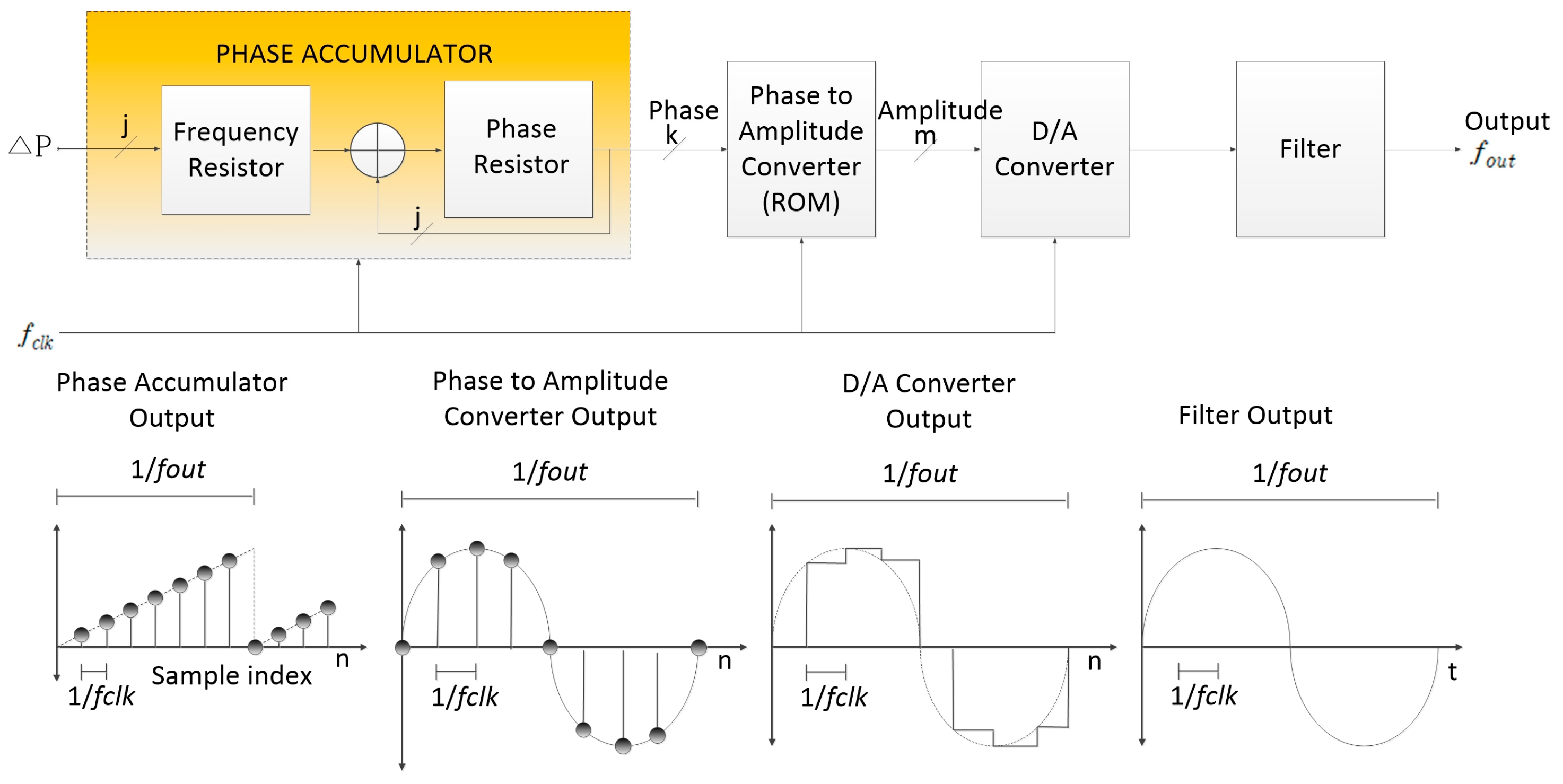
2.2. Frequency Generation by DDS
2.3. PWM Output of Frequency Generation Using DDS
3. PWM-Based Algorithm Design and Generation
3.1. Frequency Generation Using PWM
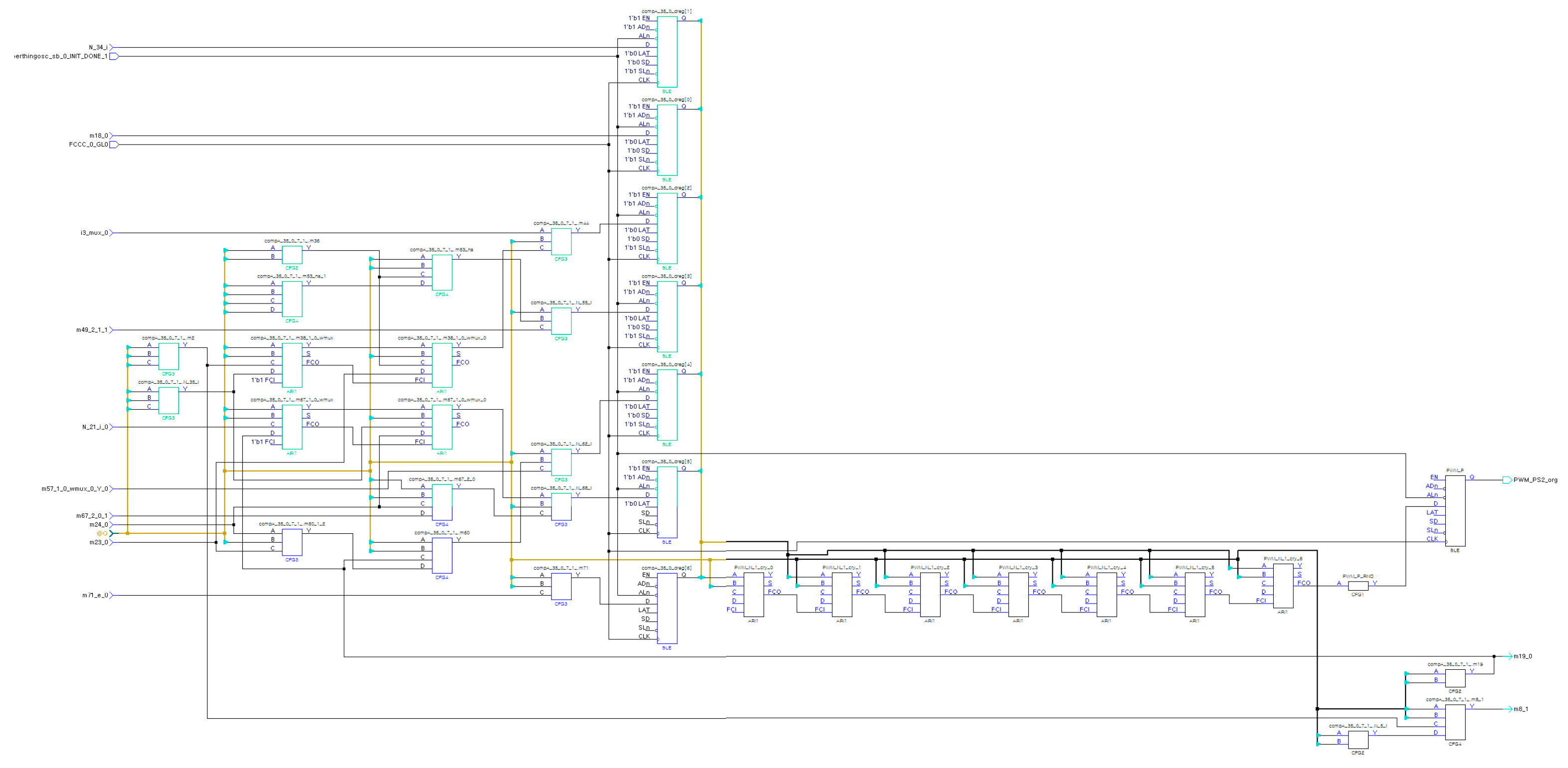
3.2. PWM-Based Algorithm Design
- Y: value for frequency calculation;
- CK: 268.435456 MHz clock;
- Fq: actual carrier frequency to be used.
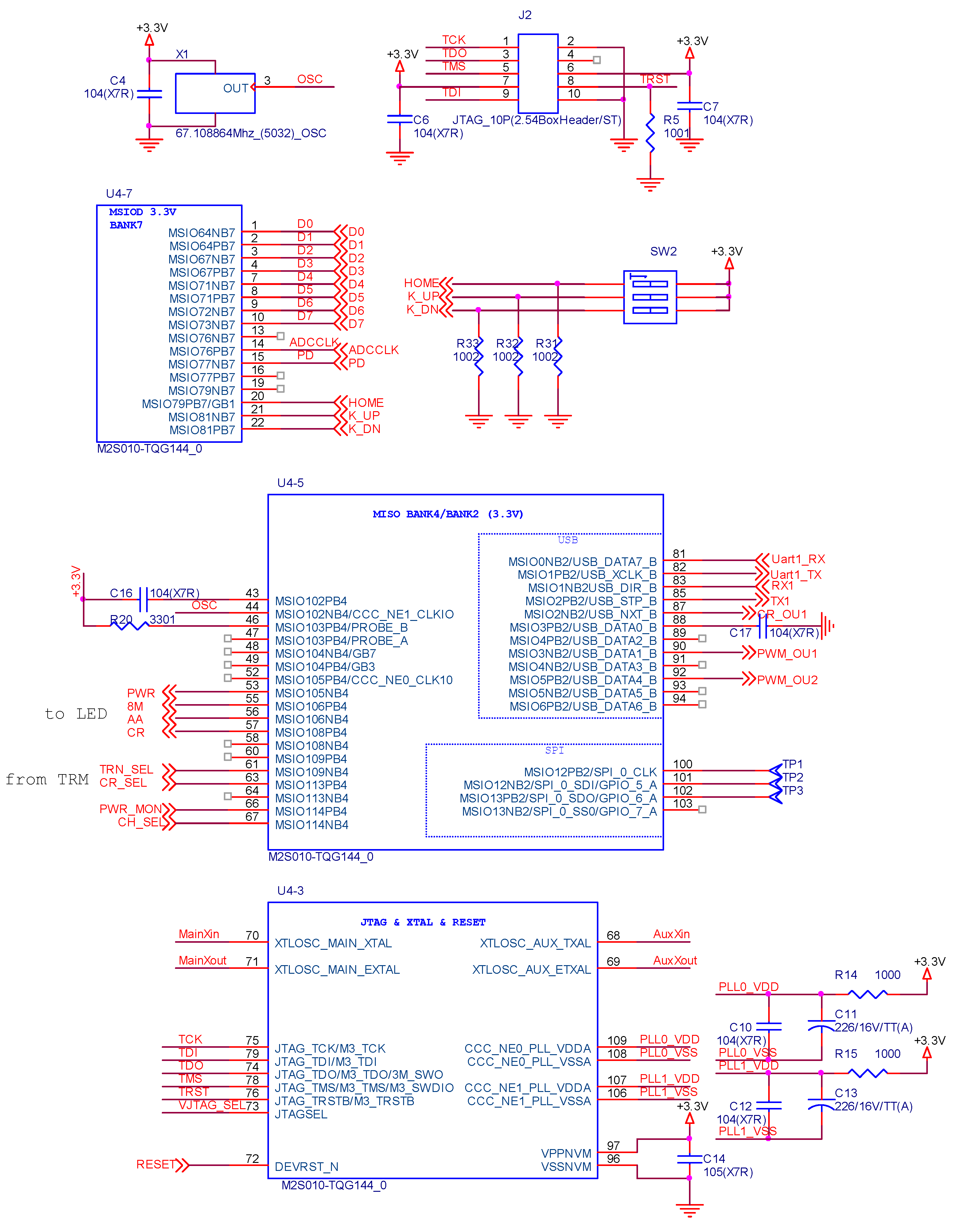
3.3. Frequency Generation Implementation
4. System Design and Fabrication
4.1. Train Stationary Stopping System Design
4.2. Design and Fabrication
4.2.1. Oscillator Module
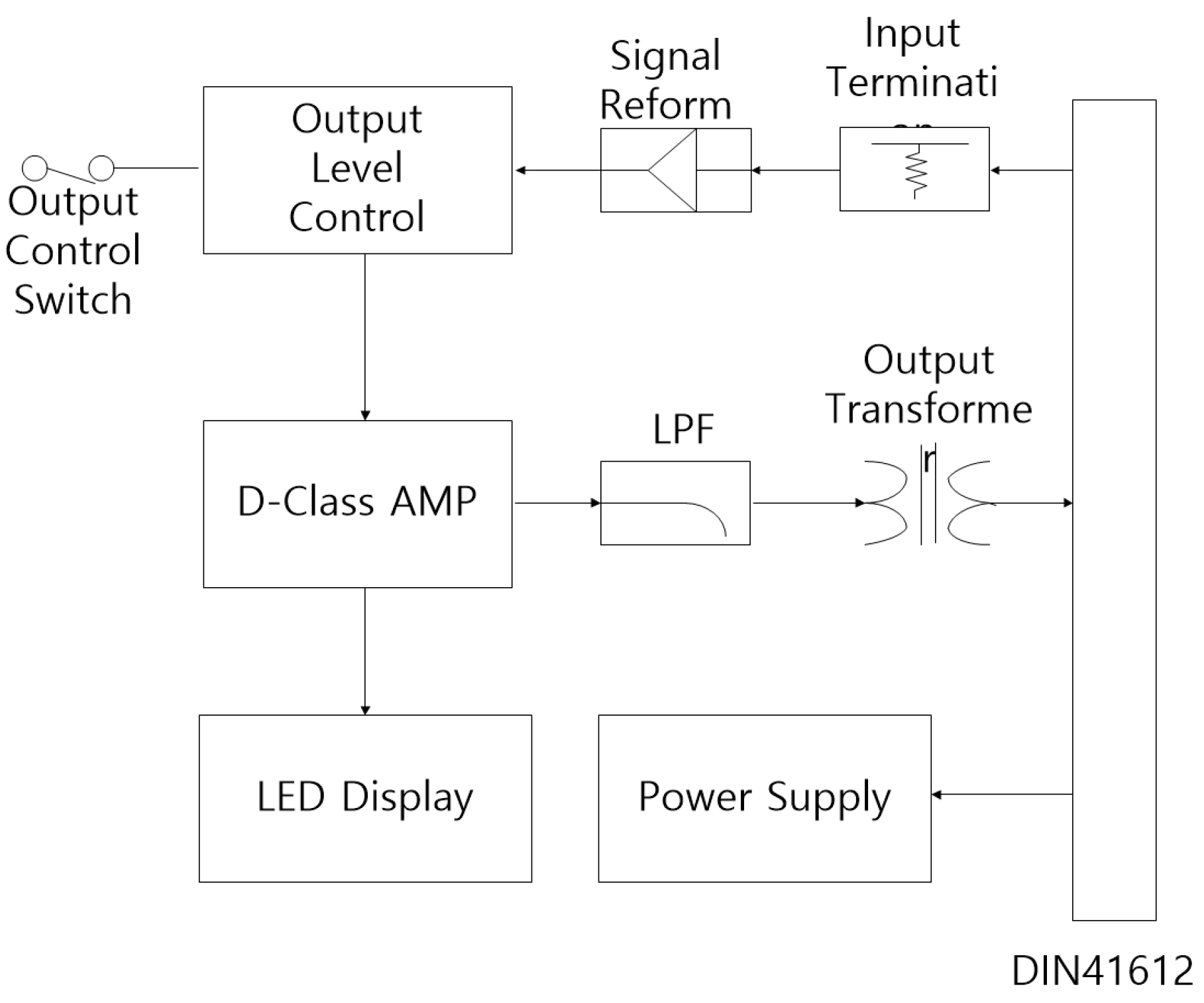
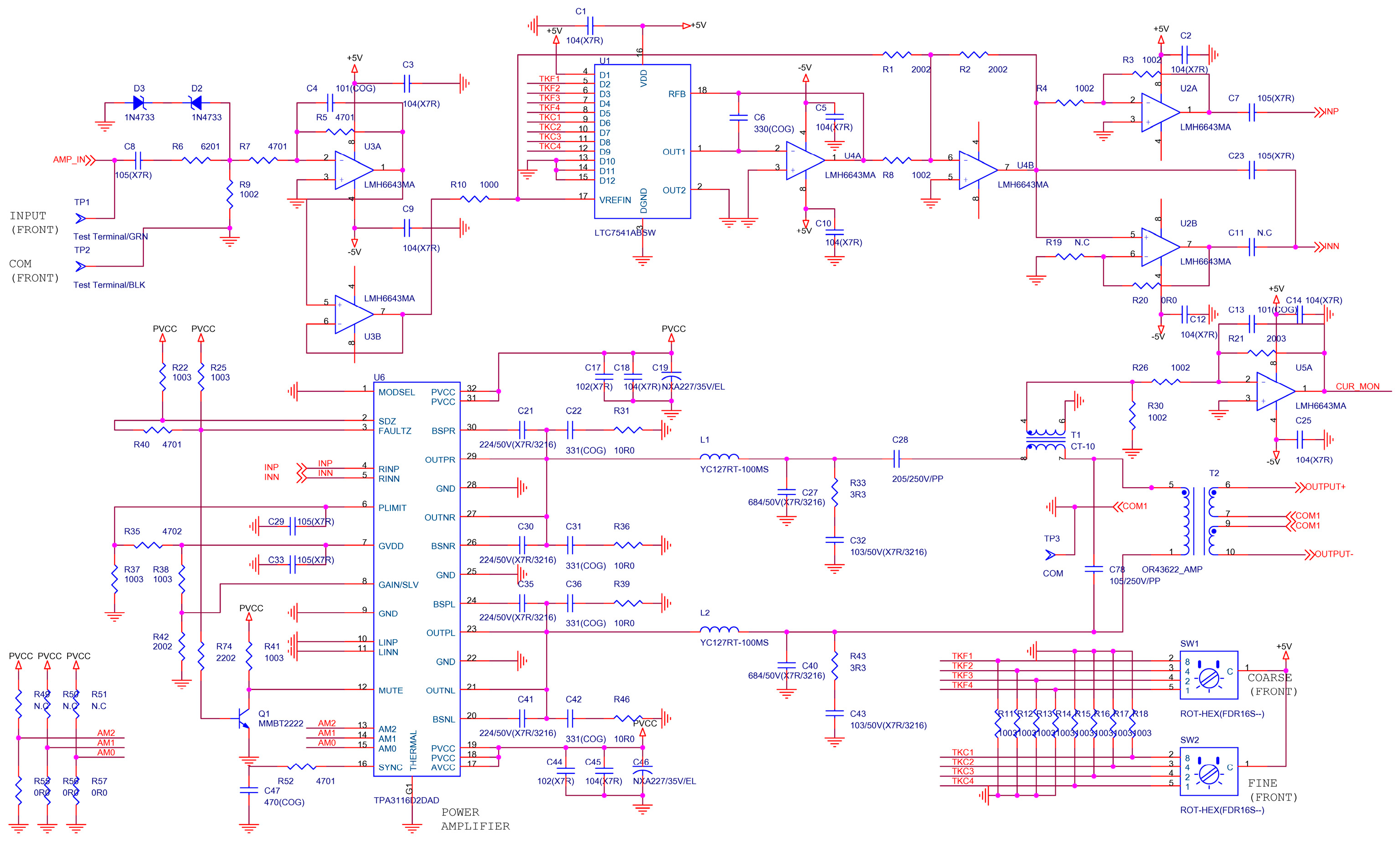
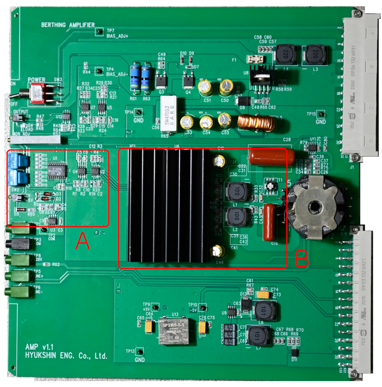
4.2.2. Amplifier Module
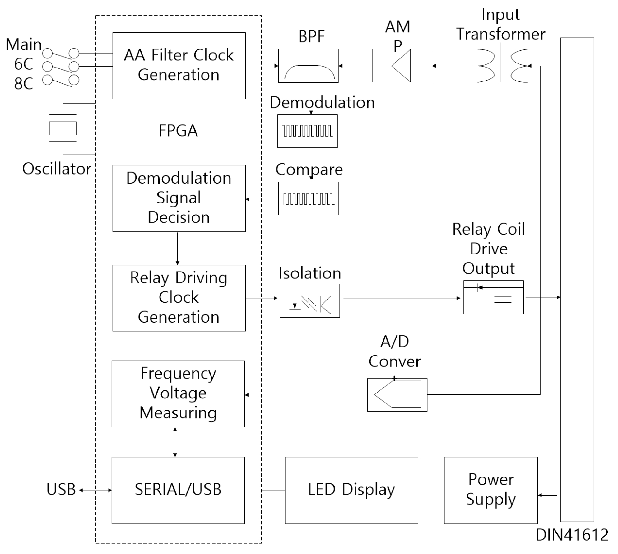
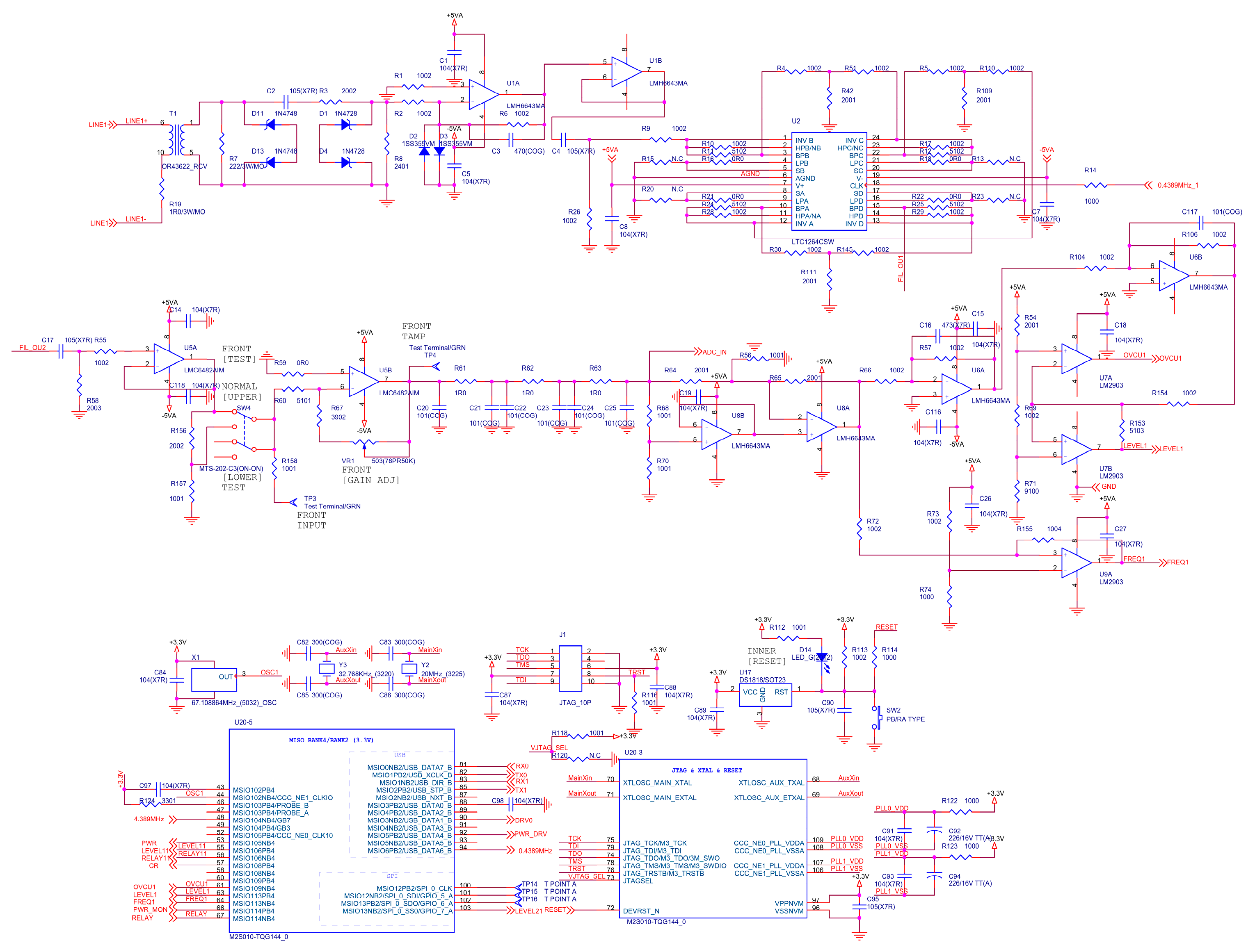
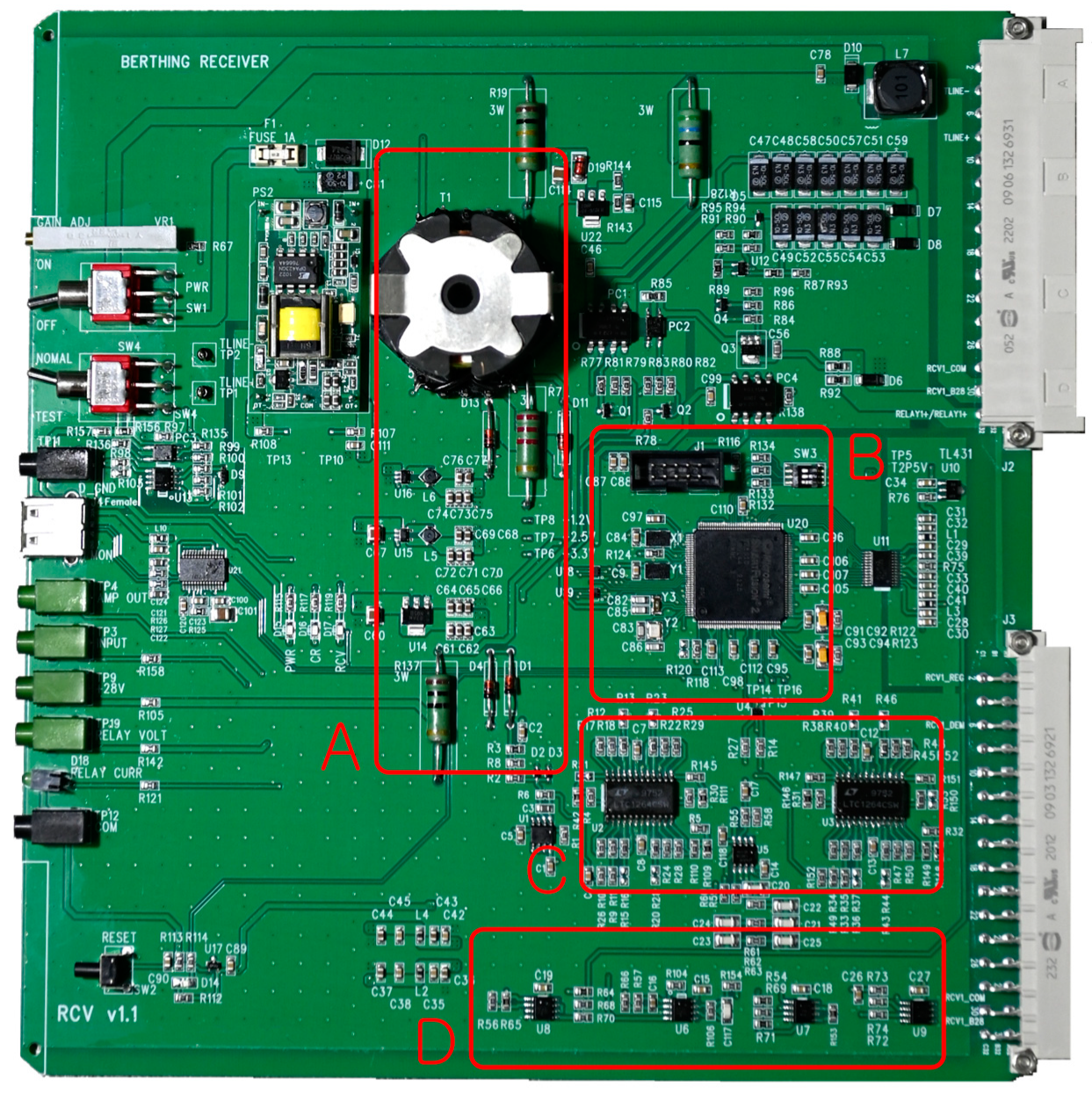
4.2.3. Receive Module
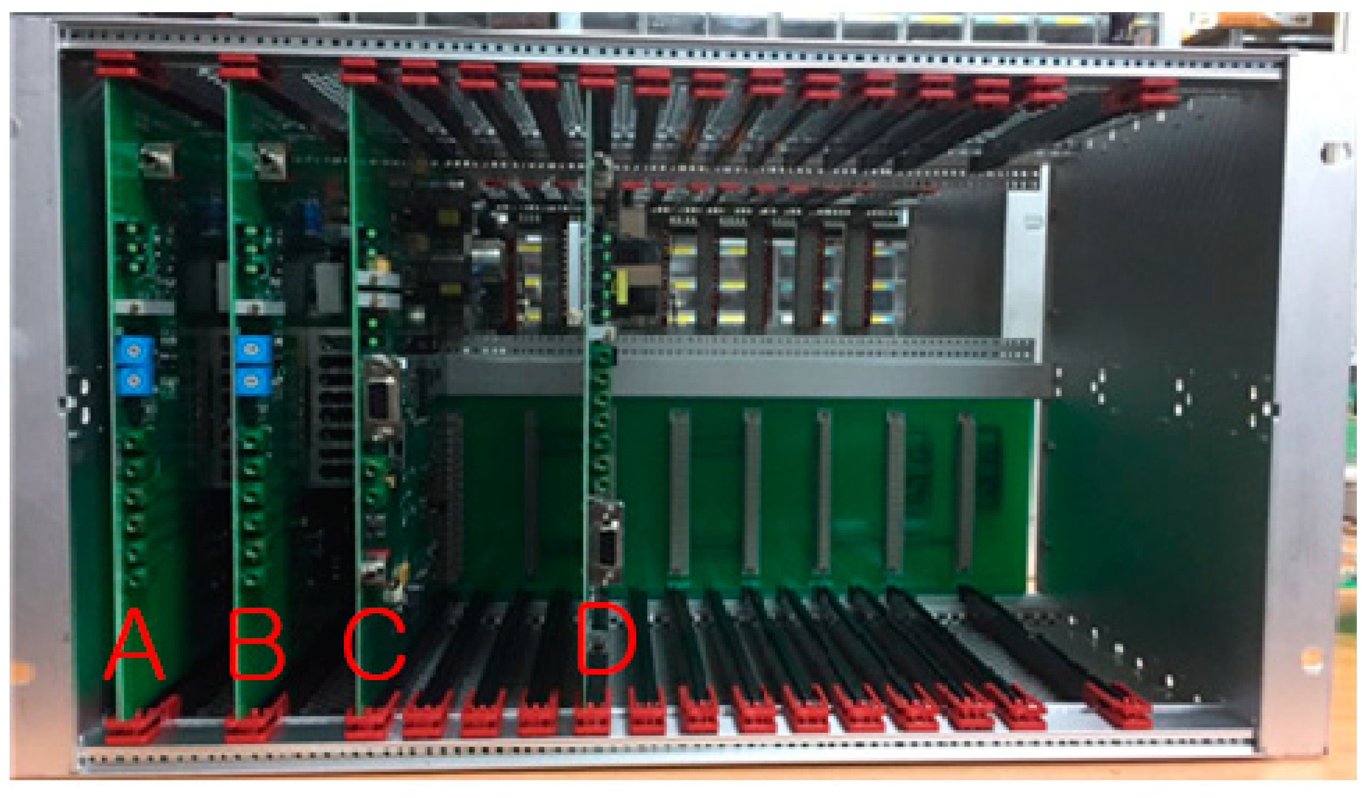
4.2.4. Completely Assembled Equipment
5. Experimentation and Verification
5.1. Laboratory Experiment
- (1)
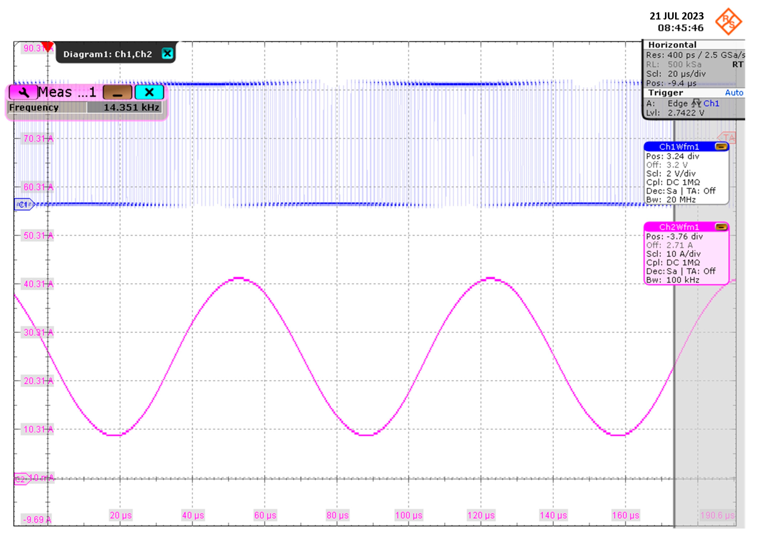
- Oscillator module experiment
- (2)
- Amplifier module experiment
- (3)
- Receive module experiment
5.2. Field Experiment
5.3. Comparison with Related Research and Existing Devices
5.3.1. Comparison with Related Studies
5.3.2. Comparison with Existing Equipment
6. Conclusions
Author Contributions
Funding
Data Availability Statement
Conflicts of Interest
Appendix A

References
- Best, R.E. Phase Locked Loops, Design, Simulation and Applications, 6th ed.; McGraw-Hill: New York, NY, USA, 2004; pp. 119–158. Available online: https://www.accessengineeringlibary.com/banary/mheaeworks/5bb530a568623331/f8d8df1b8dd53738da203ec2151b508f932be15ea9154f7990a5f69caf412180/book-summary.pdf (accessed on 24 December 2023).
- Han, J.S.; Yoon, K.; Kang, J.K. Design of Digital PLL using Binary Phase-Frequency Detector and Counter for Digital Phase Detection. J. IKEEE 2021, 16, 322–327. Available online: https://https://ieeeexlpore.ieee.org/document/8993206 (accessed on 24 December 2023). [CrossRef]
- Pisolkar, K.M.; Kore, V.; Joshi, V.; Bhurke, A. Solar PV grid connected system using Phase Lock Loop Synchronization and SPWM technique. In Proceedings of the 2019 2nd International Conference on Intelligent Computing, Instrumentation and Control Technologies (ICICICT), Kannur, India, 5–6 July 2019; pp. 846–849. Available online: https://ieeexplore.ieee.org/document/8993206 (accessed on 24 December 2023).
- Balakier, K.; Shams, H.; Fice, M.J.; Ponnampalam, L.; Graham, C.S.; Renaud, C.C.; Seeds, A.J. Optical phase lock loop as high-Q filter for optical frequency comb line selection. In Proceedings of the 2017 International Topical Meeting on Microwave Photonics, Beijing, China, 23–26 October 2017; Available online: https://ieeexplore.ieee.org/document/8168727 (accessed on 24 December 2023).
- Ouyang, T.; Xiao, K.; Lin, X.; Qiu, C.; Wang, B. A multi-phase detecting method for spurs cancellation in all digital fractional-N phase-lock loops. In Proceedings of the 2018 IEEE 61st International Midwest Symposium on Circuits and Systems (MWSCAS), Windsor, ON, Canada, 5–8 August 2018; pp. 647–650. Available online: https://ieeexplore.ieee.org/document/8623983 (accessed on 24 December 2023).
- Tang, M.; Bifaretti, S.; Pipolo, S.; Ddhano, S. A Novel Phase-lock Loop with Feed-back Repetitive Controller for Robustness to Periodic Disturbance in Three-phase Systems. In Proceedings of the 2018 IEEE Energy Conversion Congress and Exposition(ECCE), Portland, OR, USA, 23–27 September 2018; pp. 2691–2697. Available online: https://ieeexplore.ieee.org/document/8557691 (accessed on 24 December 2023).
- Tierney, J.; Radre, C.M.; Gold, B. A Digital Frequency Synthesizer. IEEE Trans. Audio Electroacoust. 1971, VU-19, 49–50. Available online: https://ieeexplore.ieee.org/abstract/document/1162151 (accessed on 24 December 2023). [CrossRef]
- Hemanth Kumar, S.N.; Venkateshappa. Design and Implementation of DDS Module on FPGA. Int. J. Adv. Trends Comput. Sci. Eng. 2021, 10, 1296–1299. Available online: https://www.warse.org/IJATCSE/static/pdf/file/ijatcse1141022021.pdf (accessed on 24 December 2023).
- Ghosh, S.M.; Dhar, A.S.; Bhunia, S. Direct Digital Frequency Synthesizer Design with Modified Parabolic Method Approximation Method. Int. J. Soft Comput. Eng. 2012, 1, 2231–2307. Available online: https://www.ijsce.org/wp-content/uploads/papers/v1i6/F0287111611.pdf (accessed on 24 December 2023).
- Strelnikov, I.V.; Ryabov, I.V.; Klyuzhev, E.S. Direct Digital Synthesizer of Phase-Manipulated Signals, Based on the Direct Digital Synthesis Method. In Proceedings of the 2020 Systems of Signal Synchronization, Generating and Processing in Telecommunications (SYNCHROINFO), Svetlogorsk, Russia, 1–3 July 2020; pp. 1–3. Available online: https://ieeexplore.ieee.org/document/9166040 (accessed on 24 December 2023).
- Liu, H.; Zhou, T.; Su, Y. A Two-dimensional MEMS Scanning Mirror Cotrol Method based on Direct Digital Synthesizer. In Proceedings of the 2019 IEEE 4th Advanced Information Technology, Electronic and Automation Control Conference (IAEAC), Chengdu, China, 20–22 December 2019; pp. 85–89. Available online: https://ieeexplore.ieee.org/document/8998008 (accessed on 24 December 2023).
- Shanthi, K.G.; Sandhiya, G.; Abinaya, K.; Sangeetha, A.; Aruna, T.; Aswini, R. Performance Analysis of Vedic Multiplier and Modified Vedic Multiplier in Direct Digital Synthesizer. In Proceedings of the 2022 3rd International Conference on Electronics and Sustainable Communication Systems (ICESC), Coimbatore, India, 17–19 August 2022; pp. 64–67. Available online: https://ieeexplore.ieee.org/document/9885340 (accessed on 24 December 2023).
- Nadir Khan, M.; Imran, M.S.; Rehan, M.; Hai, U. High Speed Direct Digital Frequency Synthesizer-(DDFS) Architecture eith Reduced ROM Structure. In Proceedings of the 2005 Student Conference on Engineering Sciences and Technology, Karachi, Pakistan, 27–27 August 2005; pp. 1–5. Available online: https://ieeexplore.ieee.org/document/4382873 (accessed on 24 December 2023).
- Baikady, A.; Uma, B.V. Area and Power Efficient Architecture for Direct Digital Frequency Synthesizer. In Proceedings of the 2021 10th International Conference on Internet of Everything, Microwave Engineering, Communication and Networks (IEMECON), Jaipur, India, 1–2 December 2021; pp. 4–5. Available online: https://ieeexplore.ieee.org/document/9689136 (accessed on 24 December 2023).
- Yi, L.; Yuan, Y.; Ningmei, Y.; Yong, G. The application of a novel direct digital frequency synthesizer for the IP core design of all digital three phase SPWM generator. In Proceedings of the IEEE The 4th International Power Electronics and Motion Control Conference, 2004. IPEMC 2004, Xi’an, China, 14–16 August 2004; Volume 2, pp. 730–733. Available online: https://ieeexplore.ieee.org/document/1375805 (accessed on 24 December 2023).
- Pietrowski, W.; Ludowicz, W.; Wojciechowski, R.M. The wide range of output frequency regulation method for the inverter using the combination of PWM and DDS. Int. J. Comput. Math. Electr. Electron. Eng. 2019, 38, 1323–1333. [Google Scholar] [CrossRef]


| Entity PWM_8M is Port(clr : in std_ logic; CLK : in std_logic; Ref_Value : in std_logic_vector(12 downto 0); PWM_P : out std_logic; PWM_N : out std_logic ) Architecture behaves like PWM_8M signal Table_Sel :std_logic_vector(5 downto 0); signal Ref_Cnt: std_logic_vector(6 downto 0); signal compA: std_logic_vectoe(7 downto 0); signal compB: std_logic_vectoe(6 downto 0); begin Table_Sel <= Ref_Value(12 downto 7); Ref_Cnt <= Ref_Value(6 downto 7); compB <= compA(7 downto 1); process(Table_Sel) begin if(clr = ‘0’)then compA <= X”80”; elsif(CLK’event and CLK=‘1’)then case Table_Sel is when “00” & X”0” => compA <= X”80”; 1 Quadrant- --Descript from “00” & X”1” to “00” & X”E” by upper method-- when “00” & X”F” => compA <= X”FE”; when “01” & X”0” => compA <= X”FF”; 2 Quadrant --Descript from “01” & X”1” to “01” & X”E” by upper method-- when “01” & X”F” => compA <= X”8C”; when “10” & X”0” => compA <= X”80”; 3 Quadrant --Descript from “10” & X”1” to “10” & X”E” by upper method-- when “10” & X”F” => compA <= X”02”; when “11” & X”0” => compA <= X”01”; 4 Quadrant --Descript from “11” & X”1” to “11 & X”E” by upper method-- when “11” & X”F” => compA <= X”74”; when others => compA <= X”80”; end case; end if; end process; |
| 1Quadrant-80, 8C, 99, A5, B1, BC, C7, D1, DA, E2, EA, F0, F5, FA, FD, FE, 2Quadrant-FF, FE, FD, FA, F5, F0, EA, E2, DA, D1, C7, BC, B1, A5, 99, 8C, 3Quadrant-80, 74, 67, 5B, 4F, 44, 39, 2F, 26, 1E, 16, 10, 0B, 06, 03, 02, 4Quadrant-01, 02, 03, 06, 0B, 10, 16, 1E, 26, 2F, 39, 44, 3F, 5B, 67, 74 |
| process(clr, CLK, Ref_Cnt,compA) begin if(clr=‘0’) then PWM_PO <= ‘0’; PWM_NE <= ‘0’; elsif(CLK’event and CLK=‘1’)then if(Ref_Cnt >= compA)then PWM_PO <= ‘1’; PWM_NE <= ‘0’; else PWM_PO <= ‘0’; PWM_NE <= ‘1’; end if; end if; end process; |
| No. | Item | Function |
|---|---|---|
| 1 | Power supply | DC 28 V 4Amax |
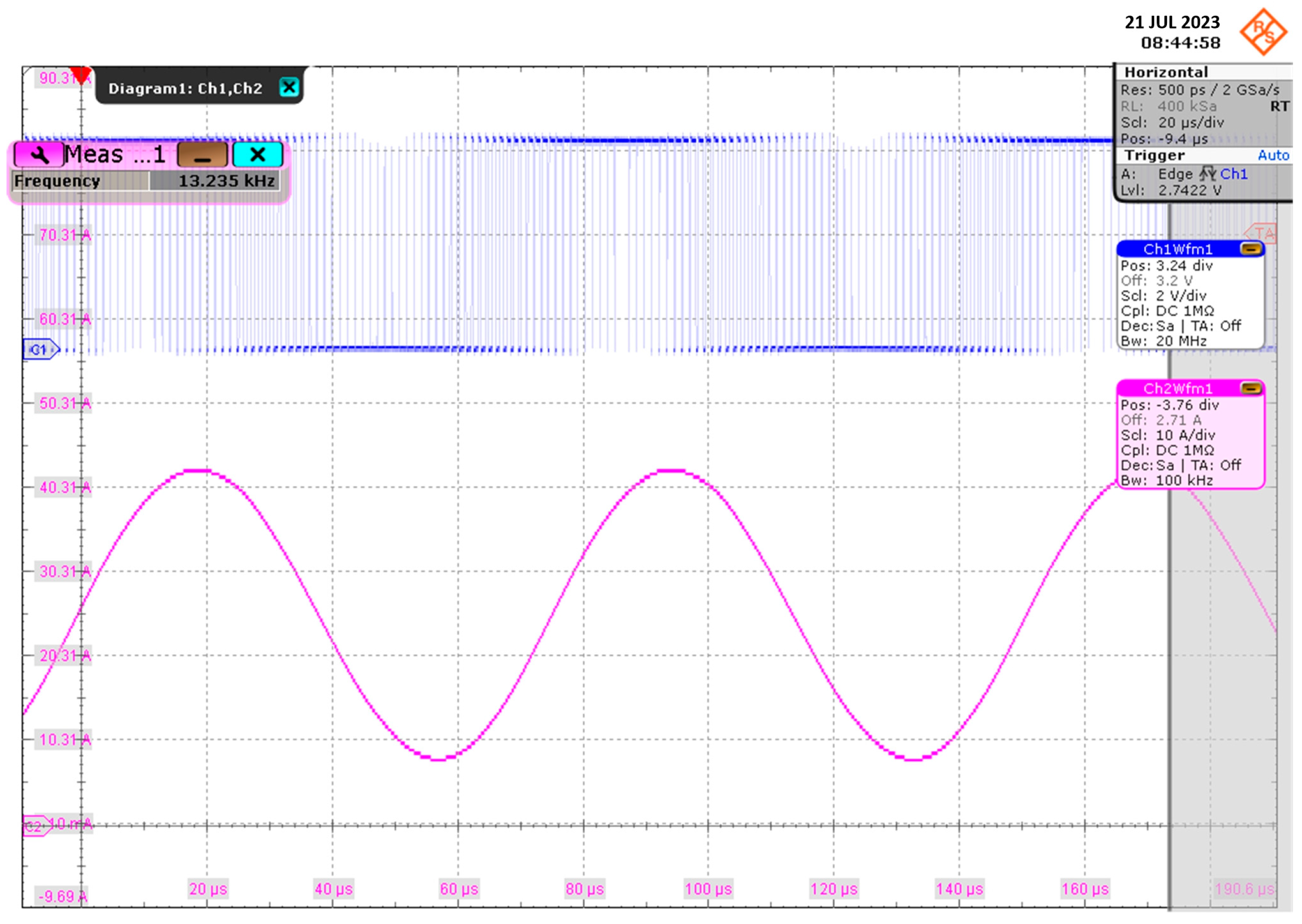
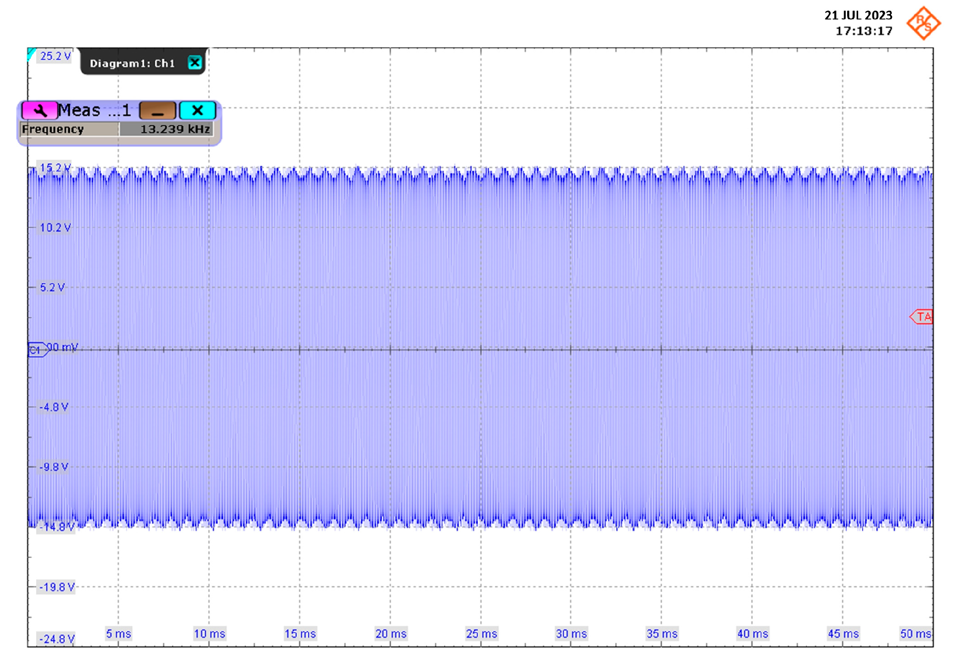
| 2 | AA Carrier Transmit Frequency | 13.235 kHz |
| 3 | AA Carrier Transmit Output | 4~10 Vrms, 50 Ω |
| 4 | 8M Carrier Transmit Frequency | 14.351 kHz |
| 5 | 8M Carrier Transmit Output | 4~10 Vrms, 50 Ω |
| 6 | AA Confirmation Carrier Transmit Frequency | 21.945 kHz |
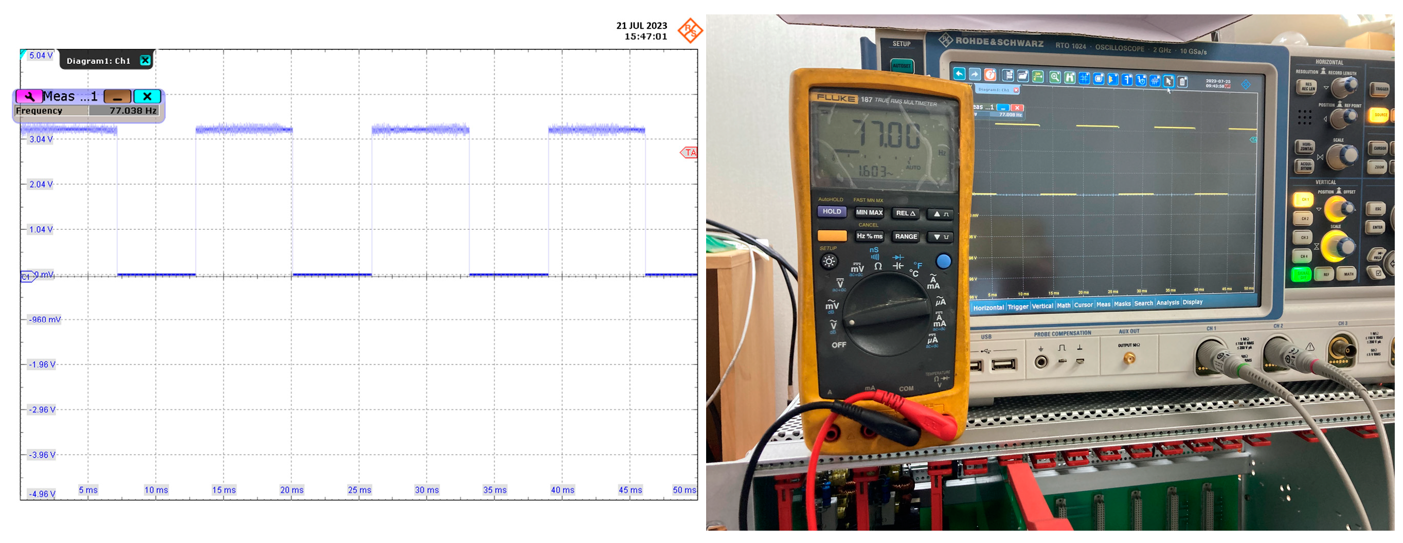
| 7 | AA Confirmation Modulation Transmit Frequency | 77 Hz |
| 8 | Receiving Relay Coil Spec. | 2100 Ω BN Relay |
| No. | Module | Item | Performance |
|---|---|---|---|
| 1 | Oscillator Module | AA Carrier Transmit Frequency with Tolerance | 13.235 kHz ± 5% |
| 8M Carrier Transmit Frequency with Tolerance | 14.351 kHz ± 5% | ||
| 2 | Amplifier Module | Input voltage and impedance | 2.76~5.4 Vrms, 1 kΩ |
| Output voltage and impedance | 11.5~23.4 Vrms, 50 Ω | ||
| 3 | Receive Module | AA Confirmation Carrier Receive Frequency with Tolerance | 21.945 kHz ± 5% |
| AA Confirmation Modulation Receive Frequency with Tolerance | 77 Hz ± 5% | ||
| BN Relay coil Drive Voltage | DC28 V, 2100 Ω |
| Item | Frequency Generation Range | Frequency Used | FPGA Implementation | Implementation Unit (Hz) | Note |
|---|---|---|---|---|---|
| DDS | Low frequency~High frequency | Some possible | 5 | [8] | |
| PLL | Low frequency ~ High frequency | Some possible with add component | 2 | ||
| PWM | Audio frequency | All possible | 1 |
| No. | Item | Unit | Target Rating | Existing Equipment Measurements | Development Equipment Measurements |
|---|---|---|---|---|---|
| Transmitter | 8M | kHz | 14.351 | 14.361 (0.69%) | 14.351 (0.009%) |
| AA | kHz | 13.235 | 13.245 (0.75%) | 13.235 (0.009%) | |
| Receive | AA Confirmation | kHz | 21.945 | 21.935 (0.45%) | 21.945 (0.009%) |
Disclaimer/Publisher’s Note: The statements, opinions and data contained in all publications are solely those of the individual author(s) and contributor(s) and not of MDPI and/or the editor(s). MDPI and/or the editor(s) disclaim responsibility for any injury to people or property resulting from any ideas, methods, instructions or products referred to in the content. |
© 2024 by the authors. Licensee MDPI, Basel, Switzerland. This article is an open access article distributed under the terms and conditions of the Creative Commons Attribution (CC BY) license (https://creativecommons.org/licenses/by/4.0/).
Share and Cite
Han, E.; Park, C.; Kim, I.; Shin, D. Research on Implementation of a PWM Generation Algorithm for Train Stationary Stopping Frequency. Electronics 2024, 13, 784. https://doi.org/10.3390/electronics13040784
Han E, Park C, Kim I, Shin D. Research on Implementation of a PWM Generation Algorithm for Train Stationary Stopping Frequency. Electronics. 2024; 13(4):784. https://doi.org/10.3390/electronics13040784
Chicago/Turabian StyleHan, Euntaek, Changsik Park, Ikjae Kim, and Dongkyoo Shin. 2024. "Research on Implementation of a PWM Generation Algorithm for Train Stationary Stopping Frequency" Electronics 13, no. 4: 784. https://doi.org/10.3390/electronics13040784
APA StyleHan, E., Park, C., Kim, I., & Shin, D. (2024). Research on Implementation of a PWM Generation Algorithm for Train Stationary Stopping Frequency. Electronics, 13(4), 784. https://doi.org/10.3390/electronics13040784