Abstract
This manuscript presents an analysis and optimization scheme for the ultra-wideband passive reconfigurable polyphase filters (PPFs) to minimize I/Q (in-phase and quadrature-phase) phase/amplitude mismatch and voltage loss. By building a mathematical model of the voltage transfer, the relationship between the resonant frequency of each stage and the I/Q mismatch and the relationship between the network impedance and the voltage loss are revealed, providing a scheme for PPF optimization. The proof-of-concept 2~8 GHz wideband reconfigurable PPF is designed in a 55 nm CMOS process. The optimization scheme enables the designed PPF to achieve an I/Q phase mismatch within 0.2439° and an I/Q amplitude mismatch within 0.098 dB throughout the entire band, and it shows great robustness during Monte Carlo sampling. The maximum voltage loss is 17.7 dB, and the total chip area is 0.174 × 0.145 mm2.
1. Introduction
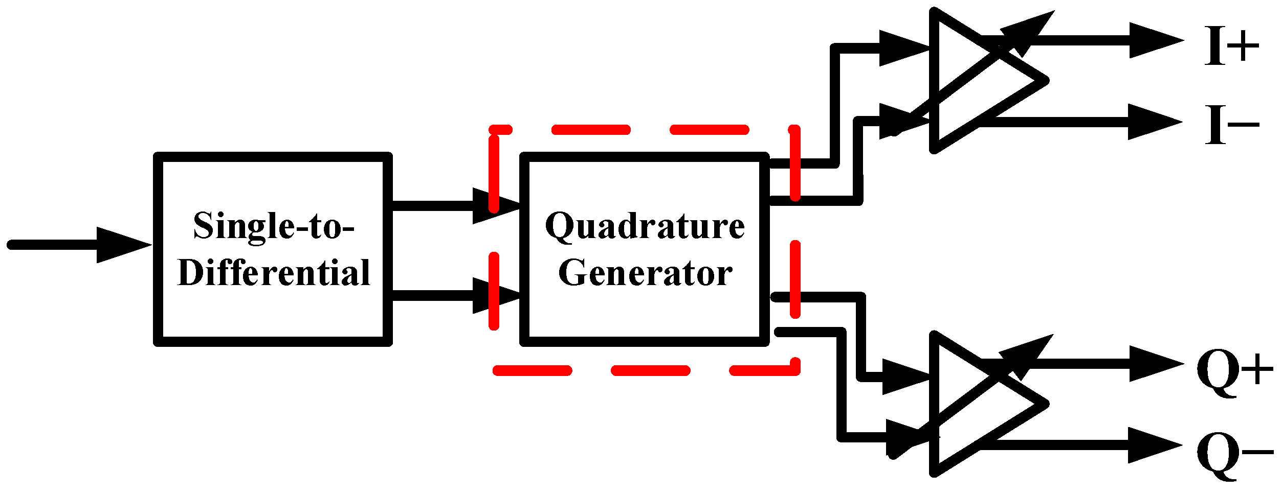
With the development of communication technology, transceivers with quadrature mixers are being used more and more widely. As all such transceivers need to provide orthogonal local carriers, the design of the in-phase and quadrature-phase signal (I/Q) generator is very important in the transceiver. Figure 1 illustrates the fundamental schematic for the local oscillator (LO). The single-phase signal is initially directed to a single-to-differential circuit to obtain differential signals. Subsequently, a quadrature generator is employed to derive I/Q signals, followed by signal amplification through a buffer.
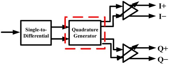
Figure 1.
Application of quadrature signal generator in LO generation circuit.
There are four main ways to generate RF quadrature signals: the RC-CR network, frequency dividers consisting of master–slave flip flops, orthogonal LC oscillators, and the polyphase network. Compared with the other three, the polyphase network is relatively insensitive to the mismatch of components and has a wider bandwidth compared to the RC-CR circuit [1]. At the same time, without an inductor in the circuit, the area is small. Moreover, it has no frequency division, which simplifies the design of the signal generator [2]. Therefore, the polyphase network has been widely used to generate I/Q signals [3,4,5,6]. As one of the polyphase networks, the PPF has attracted the attention of many researchers due to its advantages in jitter and power performance. Currently, it is commonly used for applications in Ka and lower bands.
However, there are two challenges to be solved in the PPF design: how to reduce phase and amplitude mismatch and how to reduce voltage loss. Reference [7] proposes an intermediate point compensation method to improve I/Q quadrature; it detects the variation and compensates the quadrature phase mismatch by feeding the network’s output to the intermediate point. In [8], it shorts half of the capacitors and resistors of the first stage to reduce the loss and area. In [9], it adds two inductors at the output of the PPF circuit to reduce the loss, at the cost of increasing the occupied area. However, there are few papers that discuss the performance tuning based on the PPF’s own parameters. Reference [10] delivers a mathematical model for passive PPF design; however, it lacks the cooperation with practical applications, including layout and post-simulations.
To improve the performance of the PPF from the perspective of the basic design process, based on the mathematical modeling, this paper analyses the model of the voltage transfer function of the PPF output signals at length and introduces the impact of the load. Also, some comparisons are drawn between the model in this paper and that in [10]. After that, a general design and optimization scheme for the PPF is given, including ultra-wideband PPF reconfiguration, resonant frequency decision, and voltage loss reduction, etc. And to verify the feasibility of the scheme, this paper presents a design of a reconfigurable PPF working at 2~8 GHz.
The structure of this paper is as follows. In Section 2, the basic model of the PPF is established, and the general rule of the PPF orthogonal phase error is analyzed in detail. In Section 3, the input and output impedance model of the PPF is proposed and is utilized to analyze the loss of the multistage PPF. Section 4 shows the PPF design process of 2~8 GHz broadband and gives the general process of the PPF design. Section 5 gives the results of the post-layout simulation. Finally, the conclusion is given in Section 6.
2. PPF I/Q Mismatch Model
2.1. Basic Principle of Multistage PPF
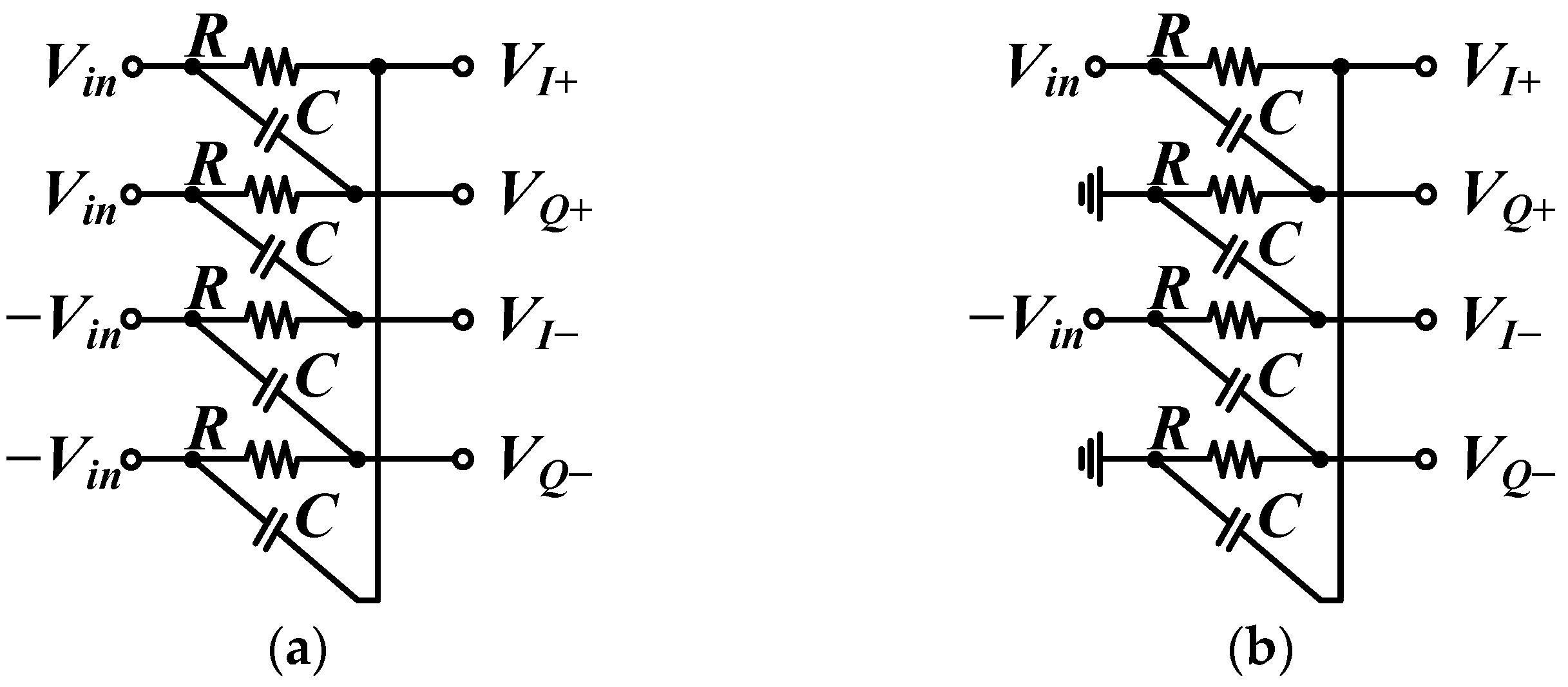
Two typical single-stage PPF structures are shown in Figure 2, one with two inputs connected together (PPF-I) and the other with two inputs connected to ground (PPF-II).

Figure 2.
Single-stage PPF: (a) PPF-I: two inputs connected together; (b) PPF-II: two inputs connected to ground.
Traditionally, for the PPF shown in Figure 2a, the equations of the four outputs are those shown in Equations (1)–(4).
Then, according to Equations (1)–(4), the output ratio of VI and VQ is
where .
Similarly, for the PPF shown in Figure 2b, the output ratio of VI and VQ is as shown in Equation (6).
From Equations (5) and (6), it is evident that the I/Q output signals in PPF-I consistently maintain their amplitude across all the frequencies but exclusively exhibit quadrature phases at the resonant frequency (1/RC). Conversely, the I/Q output signals in PPF-II retain quadrature phases at all the frequencies but share the same amplitude solely at the resonant frequency (1/RC).
Notably, although the image rejection ratio (IRR) is the commonly preferred parameter in typical measurements, the analysis in [2] underscored the PPF’s IRR dependence on the quadrature phase and amplitude mismatches in the output signals. Consequently, an intuitive observation of quadrature phase/amplitude mismatches in the output signal is presented in the analysis in the following sections instead of the IRR.
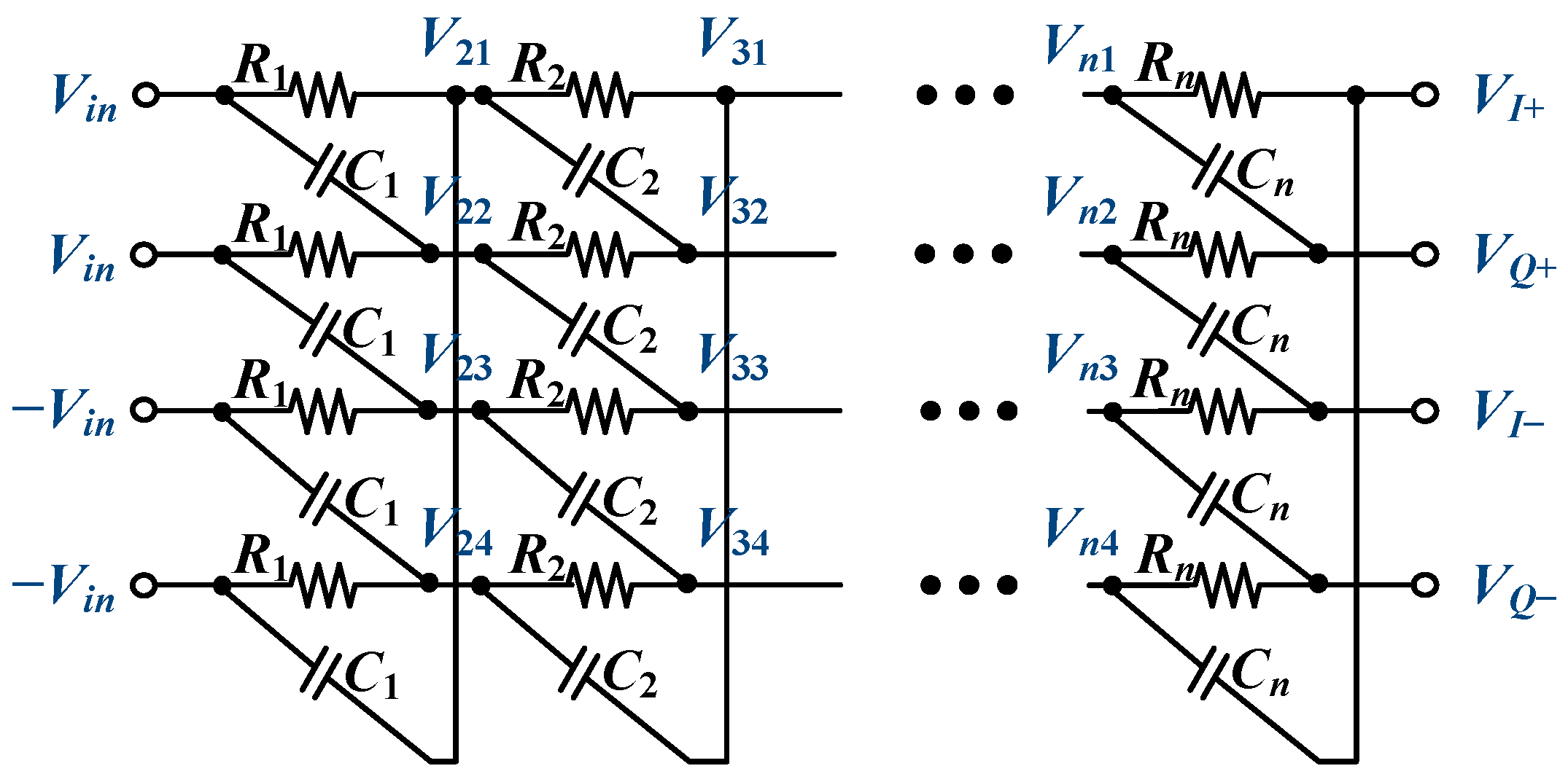
Next, advancing to the analysis of the multistage PPF, the voltage ratio between VI and VQ is determined by multiplying the matrix chains of each stage. Figure 3 illustrates the consistent multistage PPF matrix for both PPF-I and PPF-II.
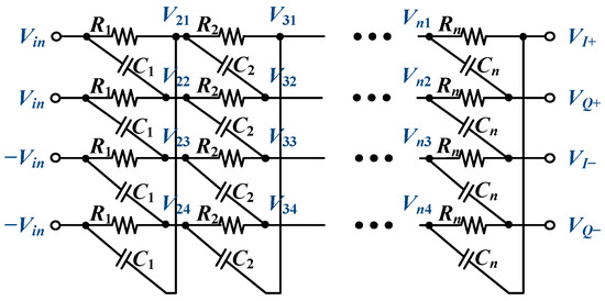
Figure 3.
Matrix of multistage PPF.
According to Figure 3, the recursive matrix can be obtained, as shown in Equation (7).
where .
The only difference is that the calculation of Vn, 1…4 for PPF-I and PPF-II is V1,1…4, which is [Vin+ Vin+ Vin− Vin−] for the former and [Vin+ 0 Vin− 0] for the latter.
Now, using Equation (7), the output signals of each stage can be calculated in both PPF-I and PPF-II. Next, the three-stage PPF is calculated and discussed based on Equation (7). However, any specific calculation process will no longer be presented in detail to ensure the succinctness of this article.
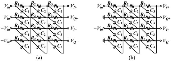
Figure 4.
Three-stage PPF: (a) PPF-I: two inputs connected together; (b) PPF-II: two inputs connected to ground.
Based on Equations (8) and (9), the phase and magnitude mismatches of the I/Q signals of two kinds of PPF are plotted as shown in Figure 5.
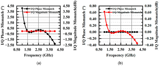
Figure 5.
I/Q mismatch of output signals in (a) PPF-I and (b) PPF-II.
From Figure 5a and Equation (8), it can be seen that for PPF-I, the I/Q output signals have the same amplitude at all frequencies and have quadrature phases at three frequency points, which correspond to the resonant frequency (1/RC) of each stage. Similarly, from Figure 5b and Equation (9), for PPF-II, the I/Q output signals have quadrature phases at all frequencies and have the same magnitude at three frequency points, which also correspond to the resonant frequency (1/RC) of each stage.
From the analysis above, neither PPF-I nor PPF-II can achieve full-band orthogonality, but they can be optimized through proper design; this is shown in the next section.
2.2. Design Scheme for I/Q Mismatch Reduction in Multistage PPF
According to Equations (8) and (9), to reduce the I/Q mismatch, resonant frequencies should play a crucial role in the multistage PPF.
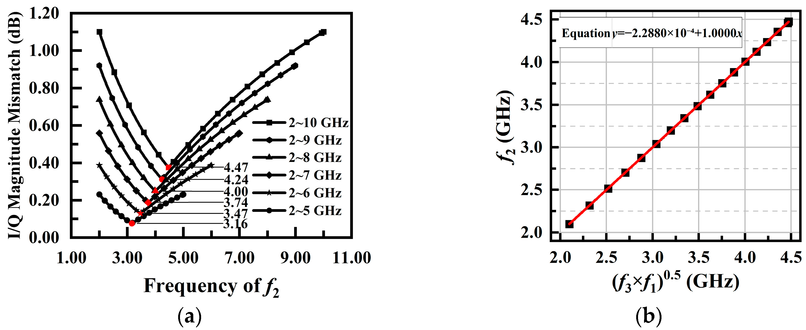
Take the structure of PPF-I as an example. In order to find the relationship between the resonant frequencies and the phase mismatch, a simulation is carried out based on Equation (8), where the intermediate frequency point (f2 = ω2/2π) is swept and the corresponding phase mismatch is obtained, under the condition that the low frequency point (f1 = ω1/2π) and the high frequency point (f3 = ω3/2π) are fixed. Note that since the magnitude mismatch theoretically remains the same for PPF-I, there is no need to analyze the magnitude mismatch in the mathematical model.
The sweeping result is shown in Figure 6a, where the pass band is also changed by increasing f3 from 5 GHz to 10 GHz to find the universality pattern. The abscissa is the frequency of f2 (in GHz), and the ordinate is the maximum I/Q phase mismatch throughout f1~f3 (in °). It can be seen that when the minimum full-band phase mismatch is achieved, f2 is always . The fitting function is shown in Figure 6b.

Figure 6.
I/Q mismatch of output signals for PPF-I: (a) relationship between f2 and maximum I/Q phase mismatch throughout f1~f3; (b) fitting function between f2 and .
Similarly, for the structure of PPF-II, the intermediate frequency point (f2 = ω2/2π) is also swept to obtain the corresponding magnitude mismatch; the result is shown in Figure 7. The fitting function is almost the same as that of PPF-I, which indicates that .

Figure 7.
I/Q mismatch of output signals for PPF-II: (a) relationship between f2 and maximum I/Q magnitude mismatch throughout f1~f3; (b) fitting function between f2 and .
Now, the conclusion is that in order to achieve good quadrature performance, whether in the structure of PPF-I or PPF-II, the intermediate frequency point ω2 should be
Analogously, for the PPF with more than three stages, to reach the lowest I/Q mismatch, the relationship between the resonant frequencies should be
It should be noted that since ω = 1/(RC), the phase mismatch is only related to the product of each resistance and capacitance, not their individual values.
2.3. Design Scheme for I/Q Mismatch Reduction in Reconfigurable Ultra-Wideband PPF
The more stages a PPF uses the larger the working band and the lower the I/Q mismatch; however, using too many stages will lead to a large voltage loss, making it a challenge for buffer design. So, for ultra-wideband application, in order to reduce voltage loss and improve I/Q quadrature performance, it is often necessary to design 2~3 PPFs parallelly, working in different frequency bands; these are selected by RF switches.
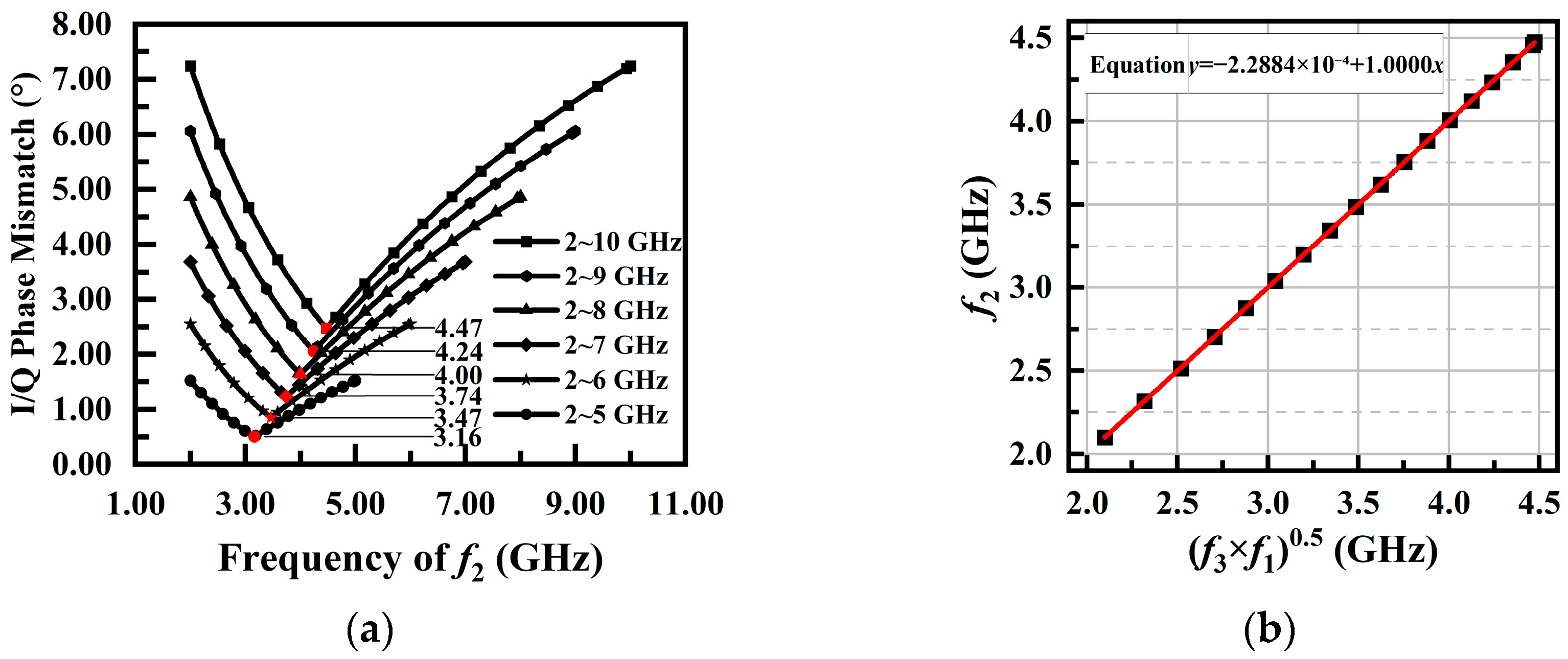
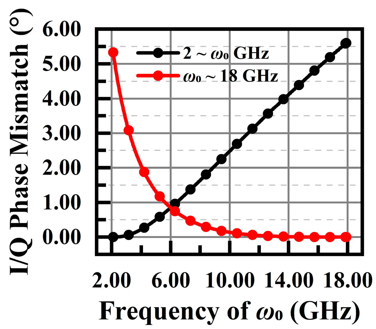
In order to achieve good orthogonality in the full pass band, the switching frequency points should also be designed at the arithmetic square root of the “high frequency points at higher frequency band” and “low frequency points at lower frequency band”. The specific proof method is similar to that in Section 2.2 and is not repeated here. Just taking one PPF-I example, suppose that two three-stage PPFs working at 2 ~ ω0 GHz and ω0 ~ 18 GHz are used to generate ultra-wideband quadrature LO signals of 2~18 GHz. Under the premise that the minimum phase mismatch is already achieved in each PPF by applying Equation (10), the frequency of ω0 is simulated; the results are shown in Figure 8.
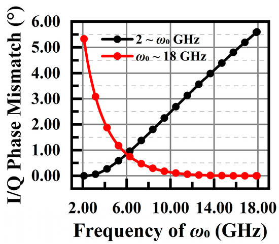
Figure 8.
Phase mismatch and segmentation frequency in 2~18 G PPF.
It can be seen that the intersection of the two curves is at 6 GHz (that is, ), indicating that when the frequency band is divided into 2~6 GHz and 6~18 GHz, the overall phase mismatch is the smallest and is about 0.8°.
According to the analysis above, for ultra-wideband PPF design, first segment the band with the switching frequency equaling the arithmetic square root of the “high frequency points at higher frequency band” and “low frequency points at lower frequency band”; then, decide the resonant frequencies of each band. The more bands that are divided, the better the orthogonality of the output in the whole band; however, it is worth noting that the frequency bands cannot be divided infinitely when considering the total area and symmetry of the layout design.
3. PPF Voltage Loss Model with Load Consideration
3.1. Impact of Load on PPF
The analysis presented in Section 2 is based on the traditional PPF analysis, which does not take into account the load of the PPF. In this section, the impact of the load is discussed.
To begin with, the load impact for the single-stage PPF is discussed. As shown in Figure 2a, the output of VI+, without considering the load, is given in Equation (12).
It can be seen that the voltage gain is always equal to 1. However, as a passive network, whether in theoretical analysis or a practical test, the PPF should have losses, and the voltage gain is bound to be less than 1. For the multistage PPF itself, the input impedance of the second stage should be regarded as the load of the first stage. If it is not large enough, losses will occur. So, traditional analysis methods cannot estimate the voltage loss of the PPF.
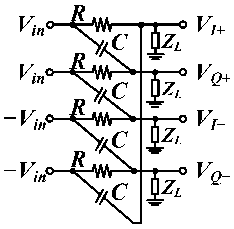
To give a more accurate function of voltage transfer, suppose that there is a load ZL connected to the output of PPF, as shown in Figure 9.

Figure 9.
Single-stage PPF with load consideration.
At point X, use Kirchhoff’s current law,
Then, the modified transfer function is
Now, the gain of the revised transfer function considering the load does not remain at one, but changes with ZL.
The analysis above proves that the load can affect the function of output signals. Remember that in Section 2, the phase mismatch is related only to the product of the resonant frequencies of each stage, when the load is not taken into account. Next, whether this conclusion changes when the load is considered should be discussed.
Continue to take the single-stage PPF as an example. Suppose that the load is ZL and that the output I/Q signals are
The ratio of the I/Q signals is
It can be seen that the ratio of the I/Q signals is independent of the load.
So, the conclusion is that the load will only affect the overall voltage loss of the PPF, not the orthogonality of the I/Q signals. We can continue to use the design schemes presented in Section 2 for a low I/Q mismatch. But to improve the performance of the PPF and to take it to a higher level, a deeper discussion on voltage loss should be conducted.
3.2. Input and Output Impedance Model
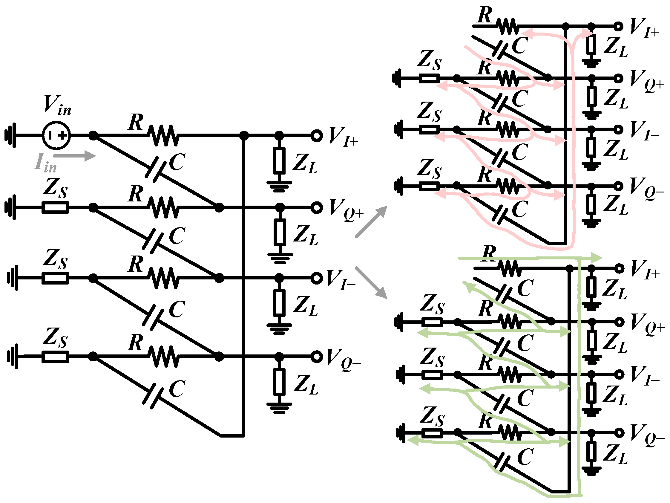
For the multistage PPF, the input impedance of the second stage participates in the part of the first stage as the load. So, to analyze the voltage transfer between the two stages, the input and output impedances of each stage need to be calculated first. The input impedance delivered in [10] neglected the source resistance at the input node, leading to a less accurate result due to the ignoring of the effects from the previous stage. In this section, a new analysis model for the impedance estimate is put forward to show the effect from the previous stage. The analysis model of the input impedance of the PPF is shown in Figure 10.
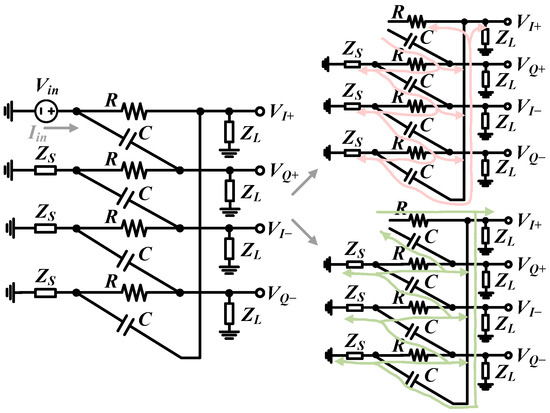
Figure 10.
PPF impedance analysis model.
As shown in Figure 10, the input impedance can be calculated as a parallel circuit of a shunt starting from the resistance R with a shunt starting from capacitance C. The shunt impedance starting from R is
The shunt impedance starting from C is
The total input impedance is
Figure 11 shows the comparison between the simulation results and the theoretical model results in the sweep, where ZS = 50 Ω, ZL = 100 Ω, R = 589 Ω, and C = 135 fF. And the curves almost overlap, indicating that the model is highly consistent with the circuit.
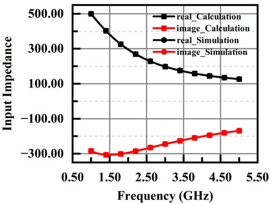
Figure 11.
Input impedance of theoretical model and simulation.
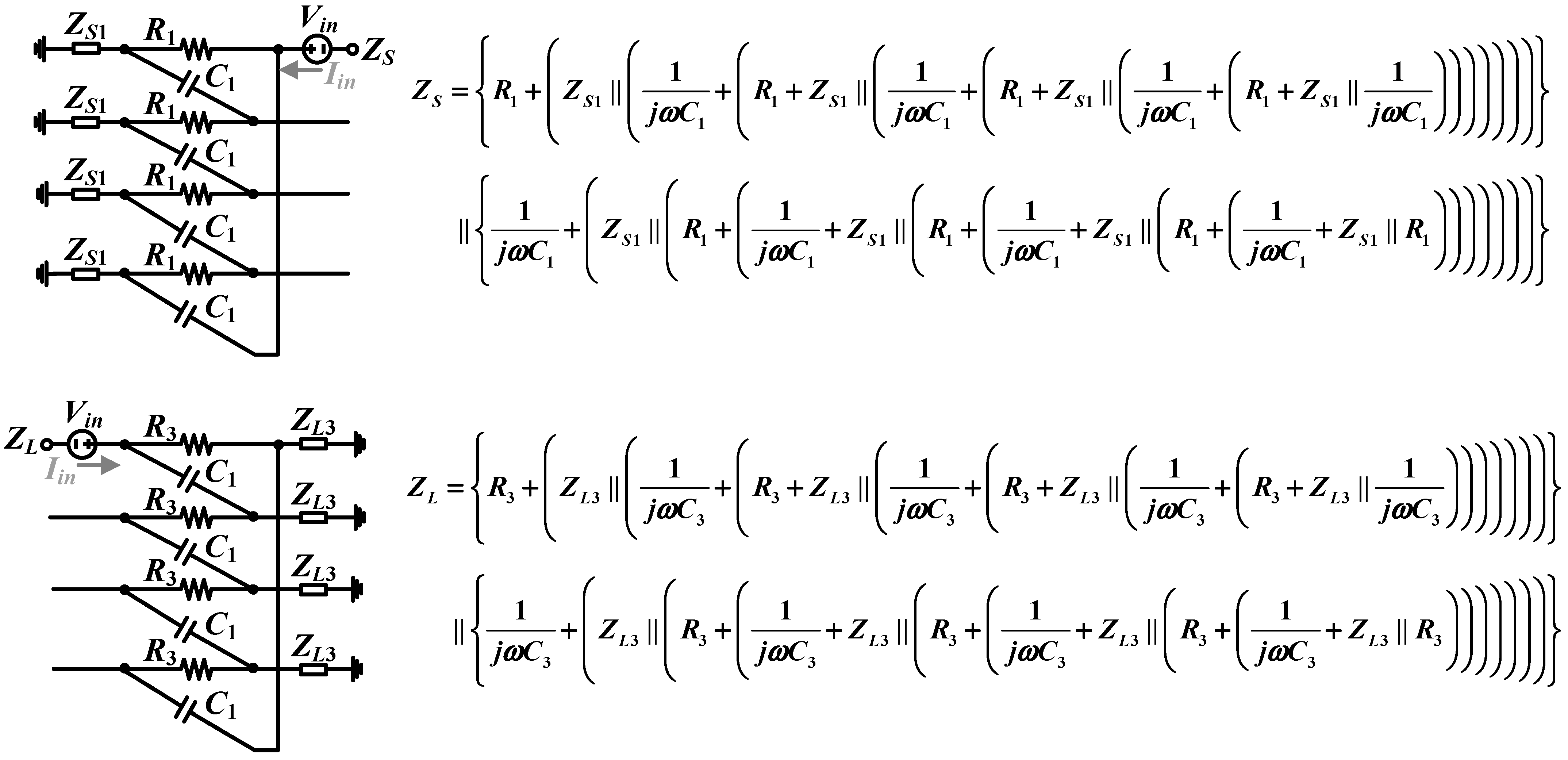
For multistage PPFs like three-stage PPF-I, to calculate the input impedance of the second stage, ZS is the impedance seen from the output node to the ground of the first stage, and ZL is the impedance seen from the input node to the ground of the third stage, which can also be obtain by Equations (18)–(20). To simplify the analysis, when calculating ZS and ZL, the first and third stages can be seen as disconnected with the second, as shown in Figure 12, where ZS1 is the impedance of the previous stage before the PPF, and ZL3 is the impedance of the next stage after the PPF.
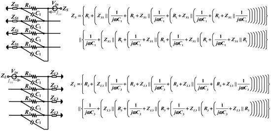
Figure 12.
Calculation of ZS and ZL for second stage.
The result will be slightly different from that of the circuit simulation, as the multistage PPF has much more complicated series or parallel branches; it can also play a part as a great estimation tool in the whole design.
Note that although the model is given by input impedance analysis, it can also be used to calculate the output impedance. The process is similar; so, it is not repeated here.
3.3. Voltage Loss Estimation of Multistage PPF
Reference [10] gives the equations of voltage loss for a certain stage of the PPF. In this section, a more universal solution is proposed for calculating the loss between any two stages, and the analysis model is shown in Figure 13.

Figure 13.
PPF Interstage loss estimation Model.
In the PPF shown in Figure 13, the second stage can be regarded as the load of the first stage, and the voltage transfer function is shown in Equations (21) and (22).
Z1 is just the input impedance of the second stage, which was discussed in Section 3.2. As for Z2, for the two-stage PPF Z2 is just the load impedance connected to the output end; in the case of three or more stages, the analysis of Z2 should also refer to the process of Z1.
In order to verify the reliability of the model with examples, the theoretical results from the analysis above and circuit simulation of a two-stage PPF are shown in Figure 14. It can be seen that the calculated results of the theoretical model are slightly larger than the simulation results of the circuit, indicating that the actual voltage transfer model of the PPF should be more complex. However, this is a feasible model for roughly estimating the output voltage; it can guide designers in setting the indicators of the whole system and can facilitate the estimation of the circuit performance at the beginning of circuit design.
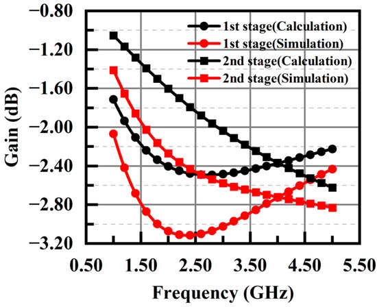
Figure 14.
Voltage loss of PPF calculated by theoretical model and circuit simulation.
Another discovery is that, according to Equations (17)–(22), the individual values of the resistance and capacitance of each stage play a significant role in the voltage loss. Therefore, although the individual values of resistance and capacitance have no influence on the I/Q mismatch, they should still be well designed to minimize the total voltage loss, according to the premise that their production remains unchanged.
4. Circuit Design: 2~8 GHz Reconfiguration PPF
According to the analysis of the phase/amplitude mismatch and the voltage loss in Section 3, a universal PPF design model can be generated. In this section, a design example of a 2–8 GHz PPF is used to detail this model.
4.1. PPF Structure Determination
As shown in Figure 2, there are two PPF structures: PPF-I, which theoretically has no magnitude mismatch, and PPF-II, which theoretically has no phase mismatch. However, if the PPF is required to have a phase mismatch that is as low as possible, it should be designed like PPF-I, as the deviation of the perfectly orthogonal frequency points caused by parasitic effects can be corrected by adjusting the designed resonant frequencies in the circuit. Similarly, if the PPF is required to have a magnitude noise that is as low as possible, it should be designed like PPF-II.
In this design, because a low phase mismatch is desired, a structure with two inputs connected together is applied.
4.2. Working Band Segmentation (Reconfiguration Modularization)
As discussed in Section 2.3, to achieve a low I/Q mismatch for the ultra-wideband application, more than one PPF working in different frequency bands should be used, and the switching frequency should be the arithmetic square root of the “high frequency points at higher frequency band” and “slow frequency points at lower frequency band”.
Therefore, for the frequency range of 2~8 GHz, two PPFs working at 2~4 GHz and 4~8 GHz, respectively, are used to form the overall circuit. Theoretically, as shown in Figure 15, the maximum phase mismatch of the whole band is about 0.22°. Band switching can be achieved by an RF switch like a transmission gate.
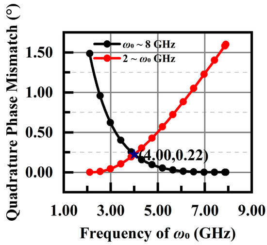
Figure 15.
Phase mismatch and segmentation frequency in 2~8 GHz PPF.
4.3. Resonant Frequency Determination of Each Stage of Each PPF
In this design, a three-stage PPF is used in each band for voltage loss and phase mismatch trade-off. According to the discussion in Section 2.2, when , the I/Q quadrature performance is the best. So, the resonant frequencies for a 2~4 G PPF are 2 GHz, 2.83 GHz, and 4 GHz; the resonant frequencies for a 4~8 GHz PPF are 4 GHz, 5.66 GHz, and 8 GHz.
4.4. R&C Determination Based on Voltage Loss
After obtaining the three resonant frequencies, the product of the resistance and capacitance at each stage can be obtained according to ω = 1/RC. According to the analysis in Section 3.3, the respective values of the resistors and capacitors play an important role in the amplitude of the output voltage of the PPF. To maximize the output voltage of the PPF, it is necessary to determine the specific values of resistance and capacitance at each stage, according to the input impedance of the output buffer and the output impedance of the input buffer.
4.5. Layout Design
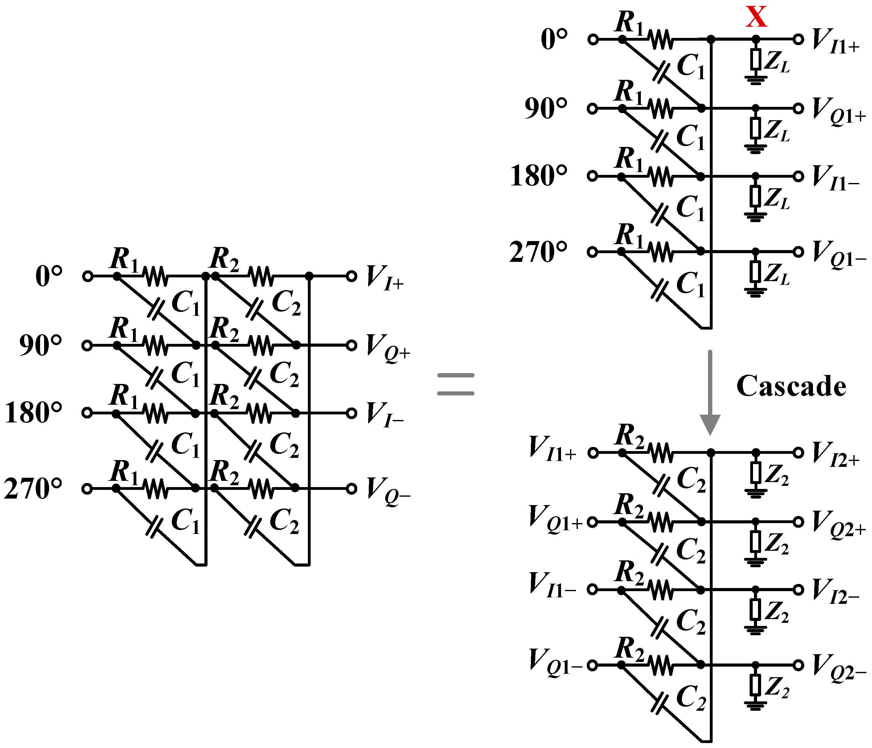
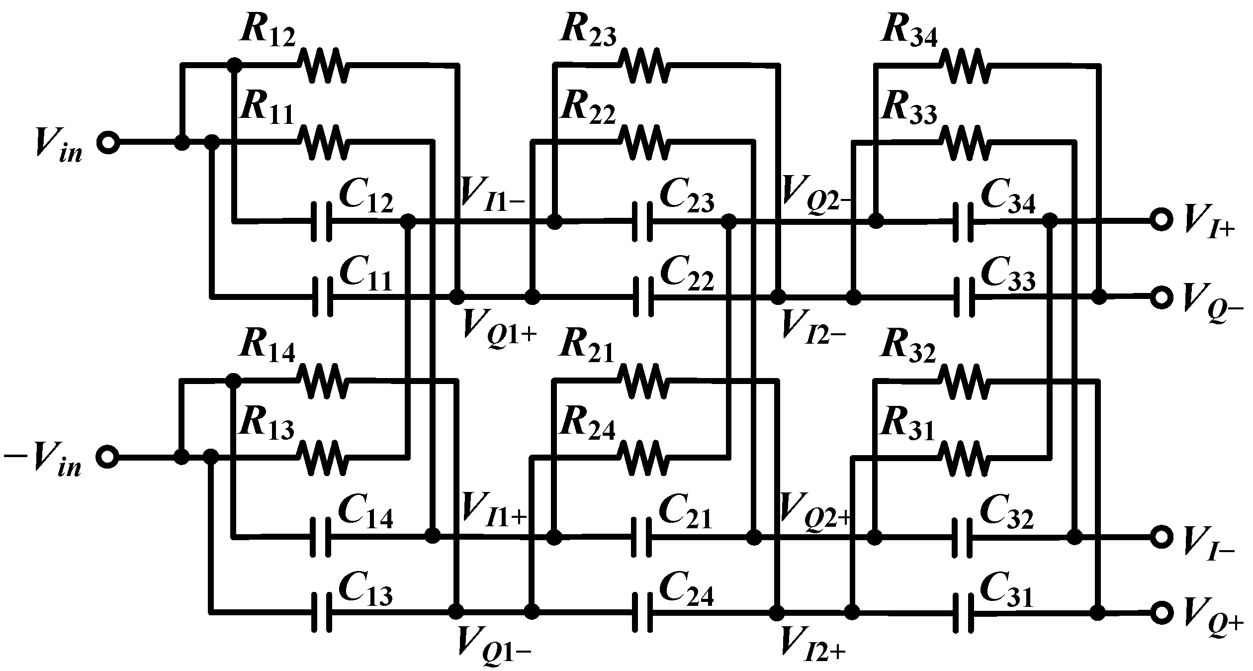
In the traditional design, the PPF layout is often drawn as a circuit schematic diagram, as shown in Figure 4, which leads to the long route between the last capacitor and the first resistance. At high frequency, long wires may have a significant parasitic inductance which is almost near the order of pH/μm. So, in the traditional layout, the length of the long wire is from tens of μm to hundreds of μm, depending on the width and length of the selected resistance and capacitor. Under the influence of this parasitic inductance and other parasitic capacitance, the required resonant frequency will be shifted.
In order to reduce this effect, the improvement proposed in this paper is to rearrange the three-stage resistors and capacitors, as shown in Figure 16; thus, the four output signals have the same routing length, as far as possible, and the parasitic influence of each route is the same, as far as possible; the overall layout is more symmetrical, reducing the influence of parasitism on the I/Q quadrature performance. And for a multistage PPF application, this routing scheme is also very convenient for cascading.
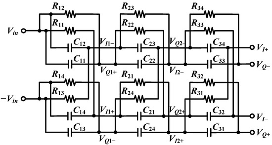
Figure 16.
Improved routing scheme of three-stage PPF layout.
As the parasitic resistance and capacitance will be connected in parallel or series with the intrinsic resistance and capacitance, resulting in the shifting of the resonant frequency, it is necessary to check whether the resonant frequencies of the three stages are too far from the desired one. If so, it is necessary to return to the schematic and adjust the resistance and capacitance.
5. Results and Discussions
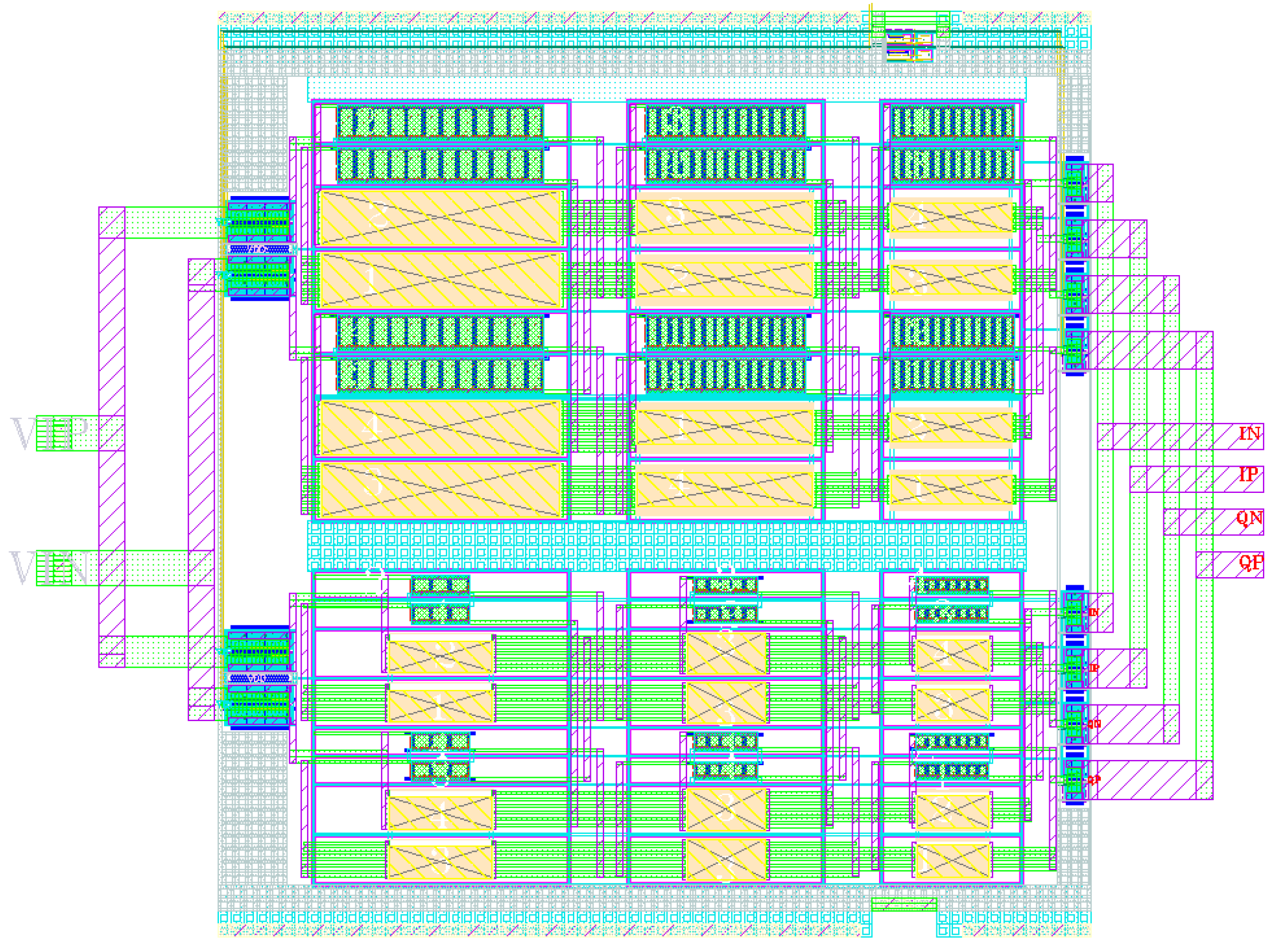
The layout of the final 2~8 GHz three-stage PPF in a 55 nm process is shown in Figure 17. The upper and lower parts work at 2~4 GHz and 4~8 GHz, respectively, and are switched by transmission gates. The area is 174 × 145 μm2. The resistors and capacitors used are shown in Table 1.
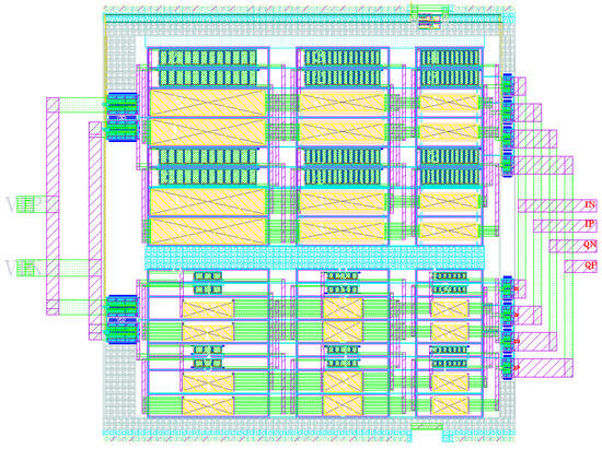
Figure 17.
Layout of PPF.

Table 1.
Parameters used in PPF.
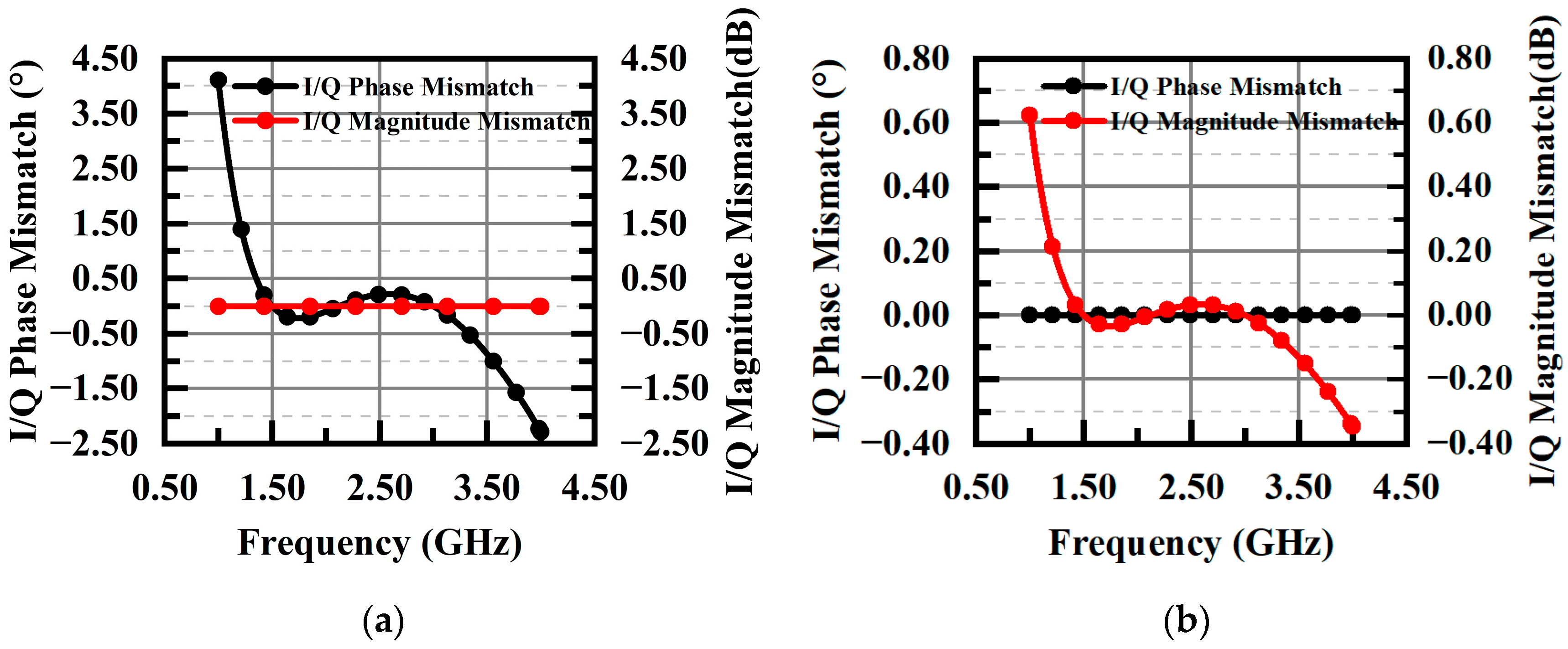
Figure 18 and Figure 19 show simulation results of post-simulation. With the output connected to an RF amplifier, whose input impedance is 30.319–292.34j throughout the 2~8 GHz frequency band, the quadrature phase mismatch is ≤0.2439°, the amplitude mismatch is ≤0.098 dB, and the voltage loss is ≤17.7 dB, in post-simulation.
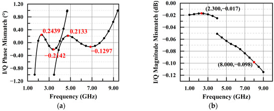
Figure 18.
I/Q mismatch for (a) phase mismatch and (b) magnitude mismatch.
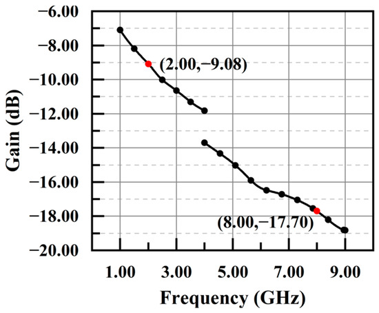
Figure 19.
Voltage gain (loss).
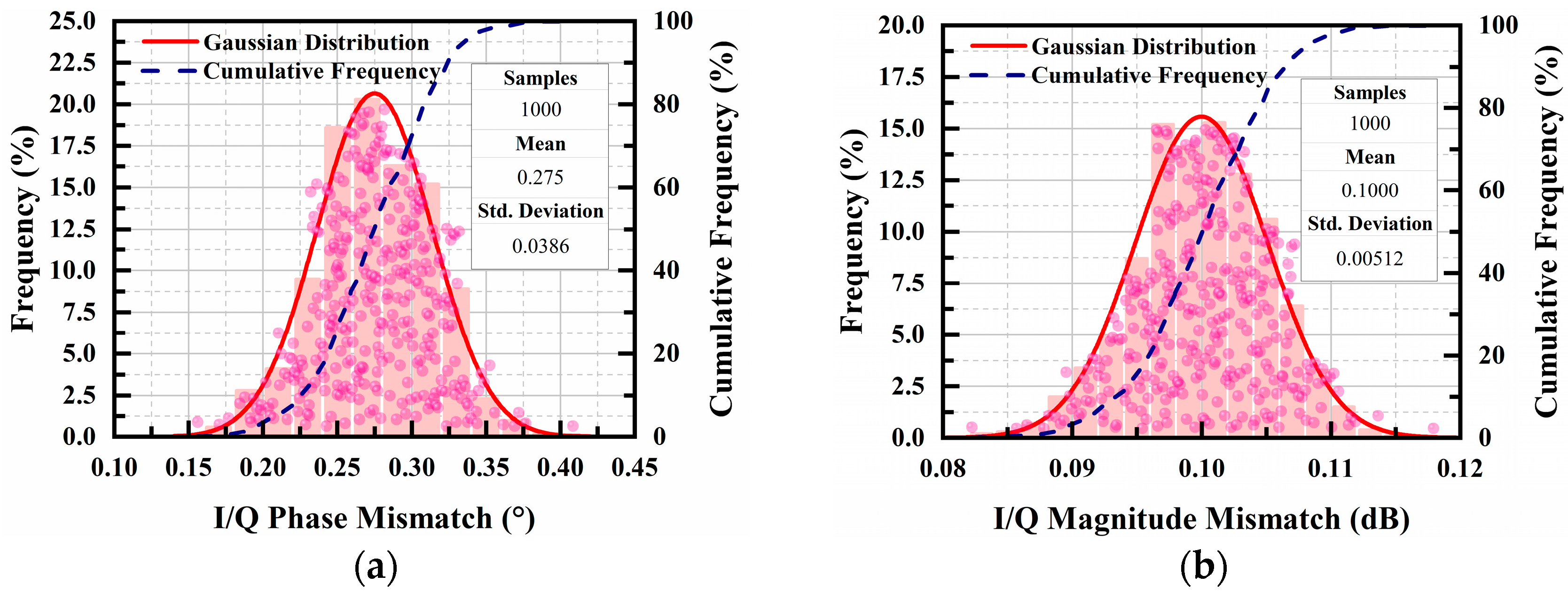
The parasitic parameter extraction was performed on the circuit layout, followed by Monte Carlo simulations and statistical fitting, as illustrated in Figure 20.
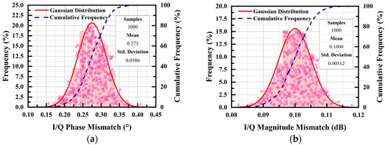
Figure 20.
I/Q mismatch in Monte Carlo sampling for (a) phase mismatch and (b) magnitude mismatch.
According to Figure 20, in the case of I/Q phase mismatch, the majority of samples are within the range of 0.225° to 0.325°, with a mean of 0.275°. Post-fitting analysis reveals an approximate adherence to a Gaussian distribution, with a standard deviation (σ) of approximately 0.0386°, and the 3σ interval of the Gaussian distribution is approximately 0.13° to 0.43°. Regarding the I/Q amplitude mismatch, most samples fall within the range of 0.095 dB to 0.105 dB, with a mean of 0.100 dB. After fitting, an approximate adherence to a Gaussian distribution is observed, with a σ of approximately 0.00512 dB, and the 3σ interval of the Gaussian distribution is approximately 0.079 dB to 0.121 dB. The foregoing analysis suggests a robustness in both the phase and the amplitude against variations in PVT and manufacturing.
The comparisons with other works in the past filter years for PPFs without buffers are shown in Table 2, indicating that the PPF designed by the method presented in this paper can achieve better performance, which has a very small I/Q mismatch with a moderated voltage loss.
Table 2.
Comparison table.
Based on this PPF, the four-phase generation network can achieve a relatively low I/Q mismatch and power consumption and can improve the overall performance of the circuit with a well-designed single-to-differential circuit and RF amplifier buffer.
6. Conclusions
This paper discusses a design and estimation scheme for a wideband reconfigurable low I/Q mismatch passive polyphase filter (PPF) in a 2~8 GHz frequency band. The relationship between the designed parameters and the PPF performance is proposed, which indicates that the key to the low mismatch lies in the proper switching frequency of the reconfigurable band and the proper resonant frequency of each stage, and the key to the low loss lies in the moderate values of resistance and capacitance, respectively. Based on this model, a 2~8 GHz band PPF is designed in a 55 nm CMOS process. The post-simulation results show that the designed PPF achieves a phase mismatch of within 0.2439° and an amplitude mismatch of within 0.098 dB within the whole frequency band. Through Monte Carlo sampling and statistical distribution fitting, the circuit demonstrates strong robustness against PVT variations and manufacturing changes. Under the load of 30.319–292.34j, it can achieve a loss of within 17.7 dB, which reduces the design difficulty of the RF amplifier buffer. The area of the whole PPF module is 0.174 × 0.145 mm2.
Author Contributions
Conceptualization, Y.W. (Yingze Wang) and X.L.; data curation, Y.W. (Yuanze Wang) and F.H.; formal analysis, Y.W. (Yingze Wang), X.L. and Y.W. (Yuanze Wang); funding acquisition, X.W. and X.L.; investigation, F.H., Z.L., X.W. and X.L.; methodology, Y.W. (Yingze Wang) and Q.Q.; project administration, X.W., X.L. and Z.L.; supervision, X.W., X.L. and Z.L.; validation, Y.W. (Yingze Wang) and F.H.; visualization, X.L. and Z.L.; writing—original draft, Y.W. (Yingze Wang) and Y.W. (Yuanze Wang); writing—review and editing, Y.W. (Yingze Wang) and X.L. All authors have read and agreed to the published version of the manuscript.
Funding
This work was supported in part by Beijing Institute of Technology Research Fund Program for Young Scholars under Grant XSQD-202105006, in part by the National Natural Science Foundation of China under Grant 62101038.
Data Availability Statement
The original contributions presented in the study are included in the article, further inquiries can be directed to the corresponding authors.
Conflicts of Interest
The authors declare no conflicts of interest.
References
- Haddad, F.; Rahajandraibe, W.; Zaid, L.; Frioui, O.; Bouchakour, R.; IEEE. Design of Radio Frequency Passive Polyphase Filter for 2.4 GHz Wireless Communication Applications. In Proceedings of the 2009 IEEE 10th Annual Wireless and Microwave Technology Conference, Clearwater, FL, USA, 20–21 April 2009; pp. 142–145. [Google Scholar] [CrossRef]
- Kulkarni, S.; Zhao, D.; Reynaert, P. Design of an optimal layout polyphase filter for millimeter-wave quadrature lo generation. IEEE Trans. Circuits Syst. II Express Briefs 2013, 60, 202–206. [Google Scholar] [CrossRef]
- Sato, L.; Shouno, K.; Tanimoto, H.; Muto, C.; Yoshino, M.; Moriyama, S.; Takahashi, C. Measurement of the Frequency Characteristics of an RC Polyphase Filter Using 4-phase Square Waves. In Proceedings of the 2022 37th International Technical Conference on Circuits/Systems, Computers and Communications (ITC-CSCC), Phuket, Thailand, 5–8 July 2022; pp. 1–4. [Google Scholar] [CrossRef]
- Sahoo, A.K.; Rawat, K. Wideband Analog Polyphase Network for Harmonic Cancellation of UHF Power Amplifier. In IEEE Transactions on Microwave Theory and Techniques; IEEE: New York, NY, USA, 2022. [Google Scholar] [CrossRef]
- Bautista, M.; Dutkiewicz, E.; Huang, X.; Nguyen, D.; Zhu, F. Quadrature Broadband Phase Shift Generation Using Passive RC Polyphase Filter for RF Front-End. In Proceedings of the 2016 16th International Symposium on Communications and Information Technologies (ISCIT), Qingdao, China, 26–28 September 2016; pp. 597–601. [Google Scholar] [CrossRef]
- Sethi, A.; Akbar, R.; Hietanen, M.; Rahkonen, T.; Pärssinen, A. A 26GHz to 34GHz Active Phase Shifter with Tunable Polyphase Filter for 5G Wireless Systems. In Proceedings of the 2021 16th European Microwave Integrated Circuits Conference (EuMIC), London, UK, 3–4 April 2022; pp. 301–304. [Google Scholar] [CrossRef]
- Xiang, X.; Gai, W.; Shi, L.; He, A.; Sheng, K. An 8–12GHz 0.92° Phase Error Quadrature Clock Generator Based on Two-Stage Poly Phase Filter with Intermediate Point Compensation. In Proceedings of the 2019 IEEE International Symposium on Circuits and Systems (ISCAS), Sapporo, Japan, 26–29 May 2019; pp. 1–5. [Google Scholar] [CrossRef]
- Momeni, M.; Moezzi, M. A Low Loss and Area Efficient RC Passive Poly Phase Filter for Monolithic GHz Vector-Sum Circuits. IEEE Trans. Circuits Syst. II Express Briefs 2019, 66, 1134–1138. [Google Scholar] [CrossRef]
- Kim, C.-W.; Lee, S.-G. A 5.25-GHz image rejection RF front-end receiver with polyphase filters. IEEE Microw. Wireless Compon. Lett. 2006, 16, 302–304. [Google Scholar]
- Kaukovuori, J.; Stadius, K.; Ryynanen, J.; Halonen, K.A.I. Analysis and Design of Passive Polyphase Filters. IEEE Trans. Circuits Syst. I Regul. Pap. 2008, 55, 3023–3037. [Google Scholar] [CrossRef]
- Su, J.-Y.; Tseng, S.-C.; Meng, C.; Wu, P.-Y.; Lee, Y.-T.; Huang, G.-W. Ka/Ku-Band pHEMT Gilbert Mixers with Polyphase and Coupled-Line Quadrature Generators. IEEE Trans. Microw. Theory Tech. 2009, 57, 1063–1073. [Google Scholar] [CrossRef]
- Tang, M.; Zhang, Y.; Pang, J.; Shirane, A.; Okada, K. A 28GHz Area-Efficient CMOS Vector-Summing Phase Shifter Utilizing Phase-Inverting Type-I Poly-Phase Filter for 5G New Radio. In Proceedings of the ESSCIRC 2022-IEEE 48th European Solid State Circuits Conference (ESSCIRC), Milan, Italy, 19–22 September 2022; pp. 333–336. [Google Scholar] [CrossRef]
- Li, Y.; Duan, Z.; Lv, W.; Pan, D.; Xie, Z.; Dai, Y.; Sun, L. A 32–40 GHz 7-bit CMOS Phase Shifter with 0.38 dB/1.6° RMS Magnitude/Phase Errors for Phased Array Systems. In 2020 IEEE Radio Frequency Integrated Circuits Symposium (RFIC); IEEE: New York, NY, USA, 2020. [Google Scholar]


Disclaimer/Publisher’s Note: The statements, opinions and data contained in all publications are solely those of the individual author(s) and contributor(s) and not of MDPI and/or the editor(s). MDPI and/or the editor(s) disclaim responsibility for any injury to people or property resulting from any ideas, methods, instructions or products referred to in the content. |
© 2024 by the authors. Licensee MDPI, Basel, Switzerland. This article is an open access article distributed under the terms and conditions of the Creative Commons Attribution (CC BY) license (https://creativecommons.org/licenses/by/4.0/).